
Strategies toward highly efficient CIGSe thin-film solar cells fabricated by sequential process
Byungwoo
Kim
 ab and
Byoung Koun
Min
*ac
ab and
Byoung Koun
Min
*ac
aClean Energy Research Center, Korea Institute of Science and Technology, Hwarang-ro 14-gil 5, Seongbuk-gu, Seoul 02792, Republic of Korea. E-mail: bkmin@kist.re.kr
bDepartment of Materials Science and Engineering, Korea University, 145 Anam-ro, Seongbuk-gu, Seoul 02841, Korea
cGreen School, Korea University, 145 Anam-ro, Seongbuk-gu, Seoul 02841, Republic of Korea
First published on 5th June 2018
Abstract
Thin-film solar cells with copper indium gallium selenide (CIGSe) as the absorber layer are considered an attractive alternative to crystalline Si-based (c-Si) solar cells due to their significant potential for low-cost solar electricity production with a minimal requirement of raw materials. The efficiency record of 22.6% was achieved recently in CIGSe solar cells, which was comparable to c-Si solar cells. However at present, only about 2% of solar panels are made from CIGSe due to its poor competitiveness in terms of production costs. On a lab scale, a one-pot 3-stage co-evaporation process is the most widely developed and utilized to obtain high-quality CIGSe films; however, this process itself is considered to be the main factor in the high production costs. A two-step sequential process, i.e., the deposition of a Cu–In–Ga metal precursor layer followed by selenization, is considered an alternative technology to decrease the production costs and increase the throughput. Thanks to a variety of efforts, this process is already being used industrially and its official record (22.3%) is almost equivalent to the highest recorded from the one-pot 3-stage co-evaporation process (22.6%). In this review, the working mechanism of CIGSe solar cells with the determining factors of the open circuit potential and current density as well as the factors affecting the efficiency in the two-step sequential process are discussed. Then, some efficiency improvement strategies consisting of three categories, namely pre-selenization, mid-selenization, and post-selenization, are discussed. Furthermore, how these strategies can be extended to much more cost-effective methods, such as solution-processed CIGSe thin-film synthesis, is also discussed. Finally, the future prospects and further efficiency improvement options are briefly outlined.
 Byungwoo Kim | Byungwoo Kim is currently a PhD student under the supervision of Prof. Woong Kim and Prof. Byoung Koun Min at the Department of Materials Science and Engineering at Korea University. He received his Bachelor's (2009) and Master's (2011) degrees from Korea University. His research interests include the fabrication of solution-processed CIG(S)Se absorbers and their applications in photoelectrochemical cells and solar cells. |
 Byoung Koun Min | Dr Byoung Koun Min received his PhD degree in 2004 from the Department of Chemistry at Texas A&M University under the direction of Professor D. Wayne Goodman. He subsequently moved to the Department of Chemistry and Chemical Biology at Harvard University as a postdoctoral fellow and worked with Professor Cynthia M. Friend until August 2006. Afterward, he started his research career as a senior research scientist in the Korea Institute of Science and Technology (KIST) and then continued his research as a principal research scientist from 2011. He is now the head of the Clean Energy Research Center in KIST and has also been appointed as a KU-KIST professor for the Green School at Korea University. His research interests are centered around solar energy conversion techniques, including thin-film solar cells and solar-chemical conversion catalysts. On the basis of these studies, he has had published more than 130 research papers in international peer-reviewed journals to date. |
Introduction
In recent years, mankind has been able to make great progress thanks to its ability to exploit the energy stored in fossil fuels accumulated over many years. However, due to rising concerns about the problems of such fuel use, such as air pollution, global warming, and the depletion of fossil fuels caused, the development of environmentally friendly energy sources is no longer considered a matter of choice but is now a necessity. Among various environmentally friendly energy sources, solar energy has proven to be one of the most promising solutions to the world's energy security concerns. Within the recent past, global PV demand has grown at a rapid pace (29.9 GW in 2012 and 78.0 GWp in 2016) and is expected to continue to grow in the future.At present, crystalline silicon (c-Si) solar cells are most widely produced and represent 90% of the global PV market.1 Meanwhile, the market share of thin-film solar cells (e.g., CIGSe solar cells) is expected to grow as next-generation solar cells due to their minimal material usage and great potential for facilitating efficiency enhancements. Another advantage of thin-film solar cells is their manufacturability on lightweight substrates in flexible shapes, thereby allowing a more expansive range of technological applications, such as building-integrated photovoltaics (BIPV) and wearable devices. However, contrary to predictions, the market share of thin-film solar cells has tended to decrease in recent years from 17% in 2009 to 7–8% in 2017.1,2 The decline in the market share of thin-film solar cells is mainly attributed to their comparatively high manufacturing cost and low efficiency compared to those of c-Si solar cells. Thin-film solar cells in their current state are yet to be considered a practical alternative to c-Si solar cells; so, the efficiency and manufacturing cost of thin-film solar cells should be improved further.
Among the various thin-film solar cells, CIGSes has attracted much attention due to their particular advantages over c-Si solar cells. Since their first development in 1976, the efficiency of CIGSe thin-film solar cells has increased more dramatically than their c-Si counterpart from just 4.5% to 22.6% in 2017.3,4 The required material usage of CIGSe solar cells is low, with a typical thickness of only 1–4 μm, which is orders of magnitude thinner than the thickness c-Si would require, i.e., ∼200 μm, due to the high absorption coefficient (>104 cm−1).5 Also, its thermal expansion coefficient makes it a more appropriate choice for locations with drastic temperature changes and its polycrystalline structure can be applied to flexible devices.1 Moreover, CIGSes have a radiation hardness that makes them exceptional for the space industry.6
The best-established technology for synthesizing quality CIGSe absorber films for high efficiency solar cells (>20%) is the vacuum-based 3-stage co-evaporation process. This technique, also known simply as a one-pot process (Fig. 1a), is able to achieve high efficiencies by intentionally forming a middle layer composed of large grains through the Cu-rich composition and a double-graded bandgap structure, where the bandgap increases toward the back and front from the middle of the absorber layer to facilitate absorption of a greater portion of the solar radiation spectrum and to facilitate separation of the photogenerated e−–h+ pairs. However, the tradeoffs are the unfavorable costs associated with the poor uniformity, the loss of expensive metal sources, the requirement for expensive vacuum equipment, etc., which impede their competitiveness in terms of the economic market.7 An attractive alternative that lowers the production cost is a sequential process that splits the fabrication into two steps, i.e., the deposition of a Cu–In–Ga metal precursor layer followed by chalcogenization with Se vapor or H2Se gas (Fig. 1b and c). The Se source can also be supplied by forming a thin Se layer deposited on the metal layer; in which case, chalcogenization is conducted under an inert gas condition.8 There are several reasons to expect lower production costs. First, the thermal energy required for crystallization is only needed during the selenization step, which is smaller compared to the thermal energy required in the one-pot process, which requires continuous heating throughout the process.7 Second, the fabrication process of the absorber layer does not require a high vacuum, which allows the production of absorbers without the use of expensive pumping equipment.9 Third, the loss of expensive In and Ga sources is minimized.10,11 In addition, co-evaporation only allows Se to be used as the chalcogen source, but a sequential process also allows sulfurization. Many companies, in a compulsion to lower the production costs, are opting to fabricate CIGSe solar cells with the sequential process instead of the one-pot process. In a recent example, Solar Frontier, a leading manufacturer of CIGSe solar cells, has already demonstrated a high performance of 22.3% certified efficiency and 23.3% uncertified efficiency with this approach.12 Other companies, such as NEXCIS and Samsung SDI, have also shown fairly high efficiencies of 17.3% and 17.9%, respectively.13,14 The 5 percentage point lead of Solar Frontier's flagship CIGSe solar cell over their competitors suggests a more nuanced approach is required to optimize the efficiency.
 | ||
| Fig. 1 Schematics of: (a) the one-pot co-evaporation process and (b) a sequential process to fabricate CIGSe films. (b) Top: sputtering process to the fabricate Cu–In–Ga precursor layer. Bottom: selenization process to chalcogenize the Cu–In–Ga precursor layer. | ||
In this article, we review methods in the sequential process that can increase the CIGSe solar cell efficiency. First, factors that affect Jsc and Voc in CIGSe solar cells fabricated by the sequential process are identified. Then, we suggest strategies to increase the efficiency in CIGSe solar cells fabricated by the sequential process.
Theoretical background
Although the sequential fabrication process is expected to result in lower fabrication costs, high-efficiency CIGSe solar cells (>20%) are mainly fabricated using the one-pot process.4,15–18 One of the main reasons for such low efficiency of the sequentially processed CIGSe solar cells is Ga accumulation toward the bottom, which lowers Voc. In CIGSe films, the bandgap is varied between 1.04 eV and 1.68 eV, depending on the Ga/(In + Ga) ratio. The bandgap of CIGSe film with respect to the composition ratio x is estimated by the equation:| Eg(x) = (1 − x)Eg(CuInSe2) + xEg(CuGaSe2) − bx(1 − x) | (1) |
 | (2) |
 | (3) |
In graded CIGSe films, on the other hand, Voc and Jsc are also influenced by the bandgap, but the depth profile must also be considered. The Voc is mainly determined by the bandgap in the SCR, without much influence from other bandgaps. Dullweber et al. showed that the Voc correlates with the maximum bandgap in the SCR where the Ga content is the highest.26 However, there was no clear correlation between Voc and the Ga content in the overall CIGSe film. On the other hand, the Jsc correlates with the minimum bandgap of the entire film. Simulations have also shown that the bandgap increase in the SCR is directly related to the Voc. According to the simulation, the increasing bandgap toward the surface increased the Voc significantly (∼7%), whereas the increasing bandgap toward the bottom layer (i.e., back grading) resulted in only a slight increase in Voc (∼0.5%). Although the increasing bandgap toward the top layer (front grading) slightly lowered the Jsc (∼1.5%), there was little effect on the efficiency. The appropriate front grading increased not only the Voc, but also the FF. However, excessively steep front grading will lower FF and Jsc because it acts as a barrier to prevent the minority carrier from diffusing into the buffer layer.27 The deterioration effect of a front grading for solar cell efficiency is especially more significant under a forward bias voltage because the narrowing SCR causes the bandgap gradient toward the surface to be steep, which exacerbates recombination losses and lowers the efficiency.28 Therefore, it is important to form an appropriate band alignment at the absorber/buffer layer interface. The appropriate CBM offset (CBM of the buffer layer minus CBM of the absorber layer) is known to be 0–0.3 (ref. 29 and 30) or 0–0.4 eV.31 When the CBM of the buffer layer is higher than that of the absorber layer (i.e., “spike”-like), the charge diffusion barrier is formed at the buffer layer/absorber layer interface. If the height of this barrier becomes greater than the appropriate value, minority carriers cannot cross over the barrier, which leads to an abrupt decrease of Jsc and FF. When the CBM of the buffer layer is lower than that of the absorber layer (i.e., “cliff”-like), recombination can easily occur between the CBM of the buffer layer and the VBM of the absorber layer, thus decreasing the Voc.32
During the selenization step of the sequential process, Ga segregation readily occurs toward the back of the film. The segregation is due to a more favorable reaction kinetics for the formation of the CuInSe2 phase, which has an activation energy of ∼124 kJ mol−1, over the formation of the CuInGaSe2 phase, which has an activation energy of ∼144 kJ mol−1.33 In addition, the formation temperature of CuInSe2 is lower than that of CuInGaSe2; CuGaSe2 is only formed at substrate temperatures above 450 °C with a reaction time of 90 min, while CuInSe2 is formed at 400 °C in 30 min.34 A study into the crystallinity of CIGSe films with the selenization temperature as the variable showed that crystalline phases containing Ga are not produced in temperatures below 410 °C.35 Furthermore, Na, which is an essential element for high efficiency CIGSe solar cells, is known to counterproductively promote the CuInSe2 formation reaction while hindering the intermixing of CuInSe2 and CuGaSe2.36 Another consequence of Ga segregation is the formation of the reverse of the desired graded structure in the CIGSe film with a reduced Ga content in the SCR, resulting in a lower Voc of CIGSe solar cells. The segregation of Ga can be mitigated by using H2Se gas instead of Se vapor or by applying a Cu-rich precursor layer.37 However, neither option completely prevents Ga segregation, but both are reluctantly considered since H2Se gas is very toxic and a high efficiency is difficult to achieve with Cu-rich compositions.
In contrast to the detrimental effect on the Voc, Ga segregation is rather advantageous for increasing Jsc due to the formation of a back surface field. Wei and Zunger showed through theory that increasing the Ga/(In + Ga) ratio will mainly increase the CBM without much effect on VBM as the CBM was 0.60 eV higher and the VBM was 0.04 eV lower when comparing CuGaSe2 to CuInSe2.38 Additional an electric field ξA was obtained by an increased Ga/(In + Ga) ratio toward the back contact, where ξA could be described by the following equation:39
 | (4) |
 | (5) |
 | (6) |
In summary, the Ga segregation, which occurs during the sequential fabrication process, is a recurring phenomenon that lowers the bandgap in the SCR, which in turn lowers the Voc but forms the back surface electric field to increase the Jsc. High-efficiency CIGSe solar cells (>20%) fabricated by the co-evaporation process have a double-bandgap graded structure with the least Ga content in the middle region and an increase in Ga content toward the surface and back contact (Fig. 2a and b). In order to fabricate a high-efficiency solar cell (>20%) by the sequential process, it is important to increase the bandgap in the SCR while keeping the back bandgap grading at a proper level. Below are some strategies that can improve the efficiency of CIGSe solar cells in the sequential process.
 | ||
| Fig. 2 (a) Comparison of the reported Ga/(Ga + In) gradings in CIGSe solar cells with an efficiency of >20%.10 Copyright 2016 John Wiley & Sons, Ltd. (b) Schematic band diagram of a CIGSe solar cell, where the Fermi level EF, space charge region (SCR), and quasi-neutral region (QNR) are indicated as well. The solid and dashed CBM lines indicate double-graded and non-graded bandgap structures, respectively. The hatched area indicates upward band bending of CBM attributed to front grading. In the double-graded structure, (1) the photogenerated electrons are transported toward the SCR due to the electric field generated by the back grading and (2) the Voc increases due to the front grading. | ||
Strategies toward high-efficiency CIGSe solar cells in a sequential process
We have categorized three strategies that can be applied to the sequential process to increase solar cell efficiency: pre-selenization, mid-selenization, and post-selenization. Pre-selenization is subdivided into vacuum-based and non-vacuum (or solution)-based metal precursor layer depositions. Mid-selenization and post-selenization mainly consist of inert gas annealing and post-sulfurization, respectively.Pre-selenization
 | ||
| Fig. 3 Schematic representation of growth models for CIGSe with various precursor layer structures: (a) In/CuGa/Mo structure, where the fabricated CIGSe film lacks Ga near the surface but this increases toward the bottom; (b) CuGa/In/Mo structure, where the fabricated CIGSe film has pinholes at the CIGSe/Mo interface; (c) multi-stack structure, where the fabricated CIGSe film has a shortage of Ga near the surface, but then the amount of Ga increases at the bottom. Here, the degree of Ga segregation is weaker than that of In/CuGa/Mo; (d) thin CuGa/In/CuGa/Mo structure, where the fabricated CIGSe film has a double-graded bandgap structure. | ||
The Mo/CuGa/In structure can prevent the formation of pinholes derived from In droplets; however, this structure has several unfavorable outcomes that would lower the efficiency of the solar cell. First, In droplets are formed on the surface during the heating process accompanying selenization, which increases the roughness of the CIGSe absorber. The high surface roughness lowers the shunt resistance and leads to a low FF. The formation of In droplets can be alleviated by stacking multiple layers of CuGa/In (Fig. 3c) instead of utilizing a simple Mo/CuGa/In structure.44 A multiple stack of 22 layers (In/CuGa/In*22) led to a higher efficiency compared to a bi- (CuGa/In or In/CuGa) or triple-layer (In/CuGa/In) structure. The increase in efficiency was mainly due to the increase in Voc and FF, presumably due to a reduced shunt density. The roughness of CIGSe fabricated from the multiple precursor layer was lower compared to that from the bi- or triple-precursor layer. The Ga gradients in the CIGSe absorber layer were similar regardless of the structure of the precursor layer, indicating that the roughness of CIGSe films, not the Ga distribution, was a main factor in determining the electrical properties of solar cells. Not only the selenized but also the as-deposited multiple precursor layers exhibited a lower roughness as well. The root mean square (RMS) of the roughness of the In/CuGa/In triple precursor layer was about three times higher than that of the (In/CuGa/In)*22 multilayer precursor structure even before selenization (221 nm and 80 nm, respectively).25 Additionally, the multilayer precursor structure improved wettability of the metal precursor layer. The triple-layer (In/CuGa/In) precursor film annealed at 580 °C caused significantly dewetting and 14.3% of the area was exposed toward the Mo substrate underneath, while the multilayer (In/CuGa/In)*22 precursor film had good coverage with only 0.8% exposure. A single Cu–In–Ga ternary target was also used instead of multiple precursor layers to obtain a uniform precursor layer and to simplify the process.46 However, the single ternary target had the disadvantage of not being able to control the composition of the film. The co-sputtering of Cu–Ga and In targets was also attempted but was accompanied by In-droplet formation.42,43 As an alternative, applying a discrete In precursor layer in a bi-layer structure can prevent the formation of droplets in the precursor layer structure of Mo/CuGa/In, resulting in improved solar cell efficiency.47
In addition to the sequence of precursor layer deposition, the composition of the entire film also greatly influences the formation of voids. The precursor composition of Cu/(In + Ga) ∼ 0.9 and Ga/(In + Ga) ∼ 0.3, which are typically accepted values for high-efficiency CIGSes, generally contain a solid solution of Ga-rich γ-Cu9(Ga,In)4 and η-Cu16(Ga,In)9 with a moderate In content and elemental In.48 Both Ga-poor and Ga-rich precursors have been proposed as causing void creation; while a Ga-poor composition easily forms In droplets, a Ga-rich composition easily forms a Ga-rich γ-Cu9(Ga,In)4 phase, which is typically observed at the rear interface and is often considered a rate-limiting step in the formation of a chalcopyrite phase.49,50 In addition, compositional changes during the selenization process should be considered since the high mobility and favorable Se reaction with In tend to form a Ga-rich phase at the rear surface.51
A direct comparison of the sequential process and the one-pot co-evaporation process showed that CuInSe2 fabricated from the sequential process had a poorer adhesion between the absorber and Mo substrate than CIGSe fabricated from the one-pot co-evaporation process, presumably due to formation of voids at the absorber/Mo interface.52 The volume expansion from the metal precursor layer to CIGSe also causes adhesion problems.53 One way to alleviate the delamination problem is to introduce Ag as a metal precursor, because AgInSe2 and AgGaSe2 have lower melting points than Cu-based chalcopyrites.54 In addition, Ag incorporation can form a (Ag,Cu)In2 phase, which also can prevent the formation of an elemental In phase.55 On the other hand, the formation of MoSe2 also affects the adhesion between the absorber and the Mo substrate. Generally, it is known that the formation of MoSe2 improves the solar cell efficiency by forming an electrical ohmic contact with the absorber,56,57 but the formation of excessive MoSe2 can induce delamination of the absorber.58 It is generally accepted that the c-axis of MoSe2 perpendicular to the Mo surface can enhance the adhesion.59,60 However, additional research is needed because one study contended that the direction of MoSe2 does not affect the adhesion.61 Various parameters, such as the selenization time,61 Na supply,62 and precursor layer conditions,62 can affect MoSe2 formation during the selenization process. In particular, MoSe2 can be formed during the subsequent sulfurization process even if MoSe2 is not formed during selenization,49,57,63 which will be discussed in detail later.
Another barrier to achieving high efficiency with a Mo/CuGa/In precursor layer structure is the In richening near the surface, which lowers the Voc of solar cells due to the lowered bandgap in the SCR. Multiple precursor layers not only inhibit In-droplet formation, but also reduce the content of In in the SCR (effectively increasing the Ga content), which increases the Voc. However, due to the Ga segregation occurring during the selenization process, the Ga content in the surface region of the CIGSe absorber becomes lower than that in the precursor layer. A combination of multiple precursor layers and low Se vapor pressure alleviates this problem.44 In an experiment, the Se vapor pressure was controlled by adjusting the temperature of the Se source, where the high Se vapor pressure was set to 470 °C and the low Se vapor pressure to 420 °C. The Ga segregation was severe under the high Se vapor pressure condition, while its extent was lower under the low Se vapor pressure condition. As a result, a high Jsc (39.22 mA cm−2) was obtained under the low Se vapor pressure. However, despite the relatively suppressed Ga segregation, the bandgap was still relatively low (1.03 eV) compared to high-efficiency (>20%) CIGSe solar cells (∼1.20 eV), resulting in a lower Voc (566 mV) and efficiency (15.5%).44
The careful control of the Se vapor pressure may mitigate but does not prevent the segregation of Ga. A CIGSe film fabricated from a Mo/In/CuGa precursor layer structure had a more uniform distribution of Ga throughout the film thickness compared to a CIGSe film fabricated from Mo/CuInGa sputtered from a single ternary target.64 However, as mentioned earlier, the Mo/In/CuGa structure is plagued with pinhole formation. On the other hand, a double-bandgap graded structure can be formed by intentionally forming a Ga-rich layer on the surface of the precursor layer because Ga has a rather low mobility in CIGSe compared to In.65 Therefore, the formation of a thin Ga-rich layer on the surface of a Mo/CuGa/In or Mo/CuInGa structure is chosen to avoid pinhole formation (Fig. 3d). This strategy usually results in a higher Voc, often increasing with FF as well, while maintaining or slightly decreasing Jsc.66–68 On the other hand, a very thin In layer (80 nm) on the bottom of the precursor layer leads to a higher efficiency by mainly increasing the Jsc without the penalty of pinhole formation. The combination of a very thin In layer on the bottom and a thin Ga layer on the surface simultaneously increases Jsc and Voc. CIGSe solar cells fabricated from a Mo/In (80 nm)/CuInGa/CuGa (125 nm) precursor structure exhibited both higher Voc (from 0.39 V to 0.46 V) and Jsc (from 29 mA cm−2 to 33 mA cm−2) values compared to solar cells fabricated from a Mo/CuInGa precursor structure, resulting in efficiency enhancement from 6.2% to 9.5%, representing about a 50% increase (Fig. 4). Here, the In layer was thin enough to form no pinholes.68 On the other hand, the Ga-rich layer on the bottom side of the precursor film also alleviated Ga segregation during selenization, which indicated that the amount of Ga in the entire precursor layer affects whether Ga segregation occurs.37
 | ||
| Fig. 4 Fabrication of a bandgap-graded CuInGaS2 solar cell by the sequential spin-coating approach. The figure was drawn based on the ref. 95. | ||
To review, Ga inside the SCR influences the Voc, whereas Ga outside the SCR affects the Jsc. In order to obtain a high Jsc (i.e., a high carrier-collection efficiency), a structure in which the Ga composition increases toward the bottom (back grading) should be formed. Both the front grading and the back grading should be carefully controlled in order to achieve high-efficiency solar cells. Wu et al. compared the effect of the Ga-rich precursor layer (CuGa) thickness near the surface of the solar cell while maintaining the overall amount of Ga in the entire precursor layer constant.45 The thickness of the top Ga-rich layer was varied to 160, 240, and 320 nm. The Voc increased as the thickness of the Ga-rich layer near the surface increased, but at the sacrifice of the Jsc. The reason was that the thick top Ga layer increases the Ga content in the SCR and but in a tradeoff with a low back grading. Since there is a tradeoff between Voc and Jsc with the thickness of the top Ga-rich layer, they should be properly balanced for maximum efficiency. The highest efficiency was obtained when the thickness of the top Ga-rich layer was 160 nm. It should be noted that when a Ga-rich layer is formed near the surface of the precursor layer, the efficiency becomes higher than that of a bi-layer (Mo/CuGa/In) or multi-layer (Mo/(CuGa/In)*5) regardless of the thickness of the Ga-rich layer.
The segregation of Ga in the bottom in the sequential selenization process is due to the formation of surface-stable CuInSe2 rather than CuInGaSe2, which pushes out Ga and eventually causes Ga to diffuse from the surface to the bottom. Preventing the formation of a selenium vacancy (VSe) mitigates the segregation of Ga toward the bottom since the diffusion of Ga during selenization is considered to occur through grain boundaries and VSe.69 Pre-feeding Se to the precursor layer before selenization suppresses the formation of VSe and consequently mitigates Ga segregation. Se can be supplied before selenization in the form of an interlayer between the precursor layer to give a Mo/In/CuIn/Se/CuGa structure.70 Pre-deposited Se was observed to inhibit the diffusion of Ga toward the substrate, which greatly increased Voc from 0.51 V to 0.67 V. However, the solar cell efficiency was low (5.86%) because the back bandgap grading was not formed and the CIGSe layer was very thin (∼500 nm). By making a few adjustments by pre-depositing Se on the surface of the precursor layer with low temperature pre-heat treatment before selenization, moderate back grading was formed while suppressing the diffusion of Ga.33 The pre-heat treatment temperature should be carefully selected since it directly affects Ga segregation. When the pre-annealing temperature was 130 °C, the Ga content in the SCR was 20% after selenization, but the Ga content decreased to 12% when the pre-annealing temperature was 200 °C. This means that the Ga segregation already proceeds during the pre-annealing. On the other hand, the film in which the pre-annealing process was omitted altogether had a Ga content of 7% in the corresponding region. The pre-heating process at 130 °C enhanced the CIGSe solar cell efficiency from 5.35% to 8.27%, which was mainly attributed to the increase in Voc (from 360 mV to 450 mV) from the alleviated Ga segregation toward the back contact. Applying a pre-annealing process at 330 °C without pre-deposition of Se also mitigated the Ga segregation by forming a binary phase, such as Cu16In9, which retards the formation of the CuInSe2 chalcopyrite structure responsible for repelling Ga toward the bottom.45
Another issue of the sequential process is the insufficient selenization of the deepest part of the absorber layer. In the one-pot co-evaporation process Se is deposited together with the metal precursor layer; whereas in the sequential process, Se is supplied after deposition of the metal precursor layer so that Se reacts from the surface of the precursor layer. It then forms a CIGSe crystal layer on the surface of the film, which prevents Se from being fed to the bottom part. To solve this problem, Se should be supplied to the bottom part before the crystallization of the surface proceeds. In this respect, pure Se or binary phases, like CuxSe or InSe, which are formed at a temperature lower than the temperature of CIGSe crystal formation, have been used to supply Se to the bottom part of the film.23,71–75 An added benefit of this technique is that the formation of InSe prevents In droplets, which are typically generated by pure In, and leads to a surface flattening of the CIGSe film. Pre-annealing in a Se vapor pressure condition is required to sufficiently form the binary Se phase from liquid Se before the selenization process. Pre-annealing is generally performed between 200 °C and 400 °C because a binary phase containing Se would not form at a lower temperature due to the melting point of Se (221 °C), while CuInSe2 crystals would develop in temperatures above this range.35 The amount of Se added to the precursor layer increases as the pre-annealing temperature increases.73 Proper pre-annealing removes the fine-grain layer of the bottom layer caused by the lack of Se, which leads to positive effects, like an increase in external quantum efficiency in the long-wavelength region75 and a reduction in shunt conductance.74 Additionally, increasing the pre-annealing temperature generally mitigates Ga segregation.74,76 Schoppe et al. conducted pre-selenization at 350 °C and 390 °C, followed by high-temperature selenization at 550 °C. The pre-selenization at 350 °C resulted in severe Ga segregation, while the pre-selenization at 390 °C formed a uniform Ga distribution.76 Without a pre-selenization process, a higher selenization temperature enhances the Ga incorporation into crystallite CIGSe grains.77 This trend has been observed not only in the sequential selenization process but also in the co-evaporation process.78
The precursor solution-based processes can be further divided into two categories; hydrazine- and non-hydrazine-based precursor methods. The solar cell efficiencies of non-hydrazine-based approaches are generally more common to have residues, like chlorine and carbon impurities, originating from each constituent of the solution, such as metal salts, binders, and solvents.83,84 The formation of impurities is regarded as detrimental to the solar cell efficiency by increasing the series resistance (Rs),85–87 interfering with grain growth,88 impeding adhesion between the absorber and substrate,87,88 and by acting as recombination centers.81 However, some conflicting reports insist that the formation of an impurity layer may enhance the solar cell performance by optimizing the absorber film composition89 and by reducing back contact recombination.90 Meanwhile, hydrazine-based approaches have shown more superior solar cell efficiencies since hydrazine decomposes into transient molecules, like N2, NH3, and H2, leaving virtually no impurity residue.91–93 Moreover, metal chalcogenide precursors can be dissolved in hydrazine, which simplifies the CIGSe absorber fabrication by allowing heating the all-inclusive precursor layer in an inert gas condition without the need for an external Se source, like Se vapor or H2Se. Recently, Zhang et al. reported a high-efficiency hydrazine-based CIGSe solar cell that was certified up to 17.3% through the deliberate synthesis of a double-bandgap graded precursor layer structure.82 The bandgap-graded structure was prepared by appropriately controlling the element ratios of the precursor solutions and by then spin-coating these solutions in order.
Although the hydrazine-based approach yields higher efficiencies, hydrazine is very toxic and explosive, so it is very cautiously considered for scale-up and commercialization. Therefore, the most ideal case would be to achieve high-efficiency solar cells with a non-hydrazine-based approach that is also competitive in practical applications. As mentioned above, one of the problems of the non-hydrazine-based approach is the presence of residual impurities. Lee et al. used a spin-coating method with nitrate-based metal salts and an alcohol-based solvent to prepare a metal precursor layer and showed that the carbon impurities could be nearly removed (<2%) by a three-step processes consisting of air annealing, sulfurization, and selenization.87 In this process, air annealing removed the carbon residues produced by the polymer binder, while sulfurization reduced the oxidized metal precursor layer during the air annealing step. Recently, the same group achieved an 11.7% efficiency without ARC and 12.3% efficiency with ARC using methanol as the solvent and polyvinyl acetate as the binder.94 The high efficiency was attributed to the naturally formed double-graded bandgap structure during the chalcogenization process with H2S/Se vapor gas. However, the external quantum efficiency was limited at longer wavelengths (>600 nm) due to the formation of a fine-grain layer at the bottom with this method and this issue is yet to be resolved.
Sequential spin-coating approaches using precursor solutions with controlled element proportions could be an attractive way to tune a bandgap gradient. Park et al. demonstrated that a bandgap gradient could be intentionally created through utilizing sequential spin-coating approaches (Fig. 4).95 Two types of solution were used to form the bandgap gradient: one containing a Cu–In–Ga precursor and the other a Cu–In precursor. When the Cu–In–Ga precursor layer was coated first and the Cu–In layer was coated later, a back bandgap grading structure with a high bandgap at the bottom was formed after selenization. This indicated that the bandgap-graded structure could be tuned by adjusting the composition of the precursor solutions. The highest efficiency of 7.29% with the Mo/CuInGaS2/CuInS2 absorber layer structure was attributed to the back gradient.
The precursor layer can be made by selecting and combining the desired properties of different solvents and binders with solutions of different compositions. For example, a low viscosity precursor solution prepared using polyvinyl acetate binder could produce a dense grain with high efficiency but requires multiple coating-and-drying cycles to obtain a proper absorber film thickness. On the other hand, a single coating-and-drying process was sufficient to achieve a proper film thickness with a high viscosity precursor solution prepared using the ethyl cellulose binder, but a solar cell fabricated using this solution suffered from low efficiency due to a high leakage current caused by the resulting porous film structure. A combination of stacking layers with a low- and high-viscosity precursor solution can reduce the number of coatings necessary while achieving a moderate solar cell efficiency at the same time. An et al. reported that a dense bottom film and a porous top film showed a highly enhanced efficiency (4.66%) compared to the cell with a film having only a porous structure (2.90%).96 Such results have been confirmed in other articles.97,98
Mid-selenization
The bottom segregated Ga formed during the selenization process can be diffused uniformly throughout the absorber film by a suitable annealing process in an inert gas atmosphere (Fig. 5). Since Ga segregation occurs during the selenization process, the homogenization of Ga should proceed after the selenization process. When an inert gas annealing process is involved, the selenization process generally consists of three steps; the initial selenization, the inert gas annealing, and chalcogenization (either selenization or sulfurization). In the first-stage selenization, it is important to obtain a low crystallinity and incomplete selenization of the CIGSe film because this facilitates the diffusion of Ga in the subsequent annealing step in an inert gas.63,99 Therefore, the first-stage selenization proceeds at a relatively low temperature (400 °C) or for a short time. In the subsequent inert gas annealing, Ga segregated at the bottom is diffused toward the surface. The selenization (or sulfurization) in the final stage proceeds at a relatively high temperature (>500 °C) to obtain a high CIG(S)Se crystallinity.49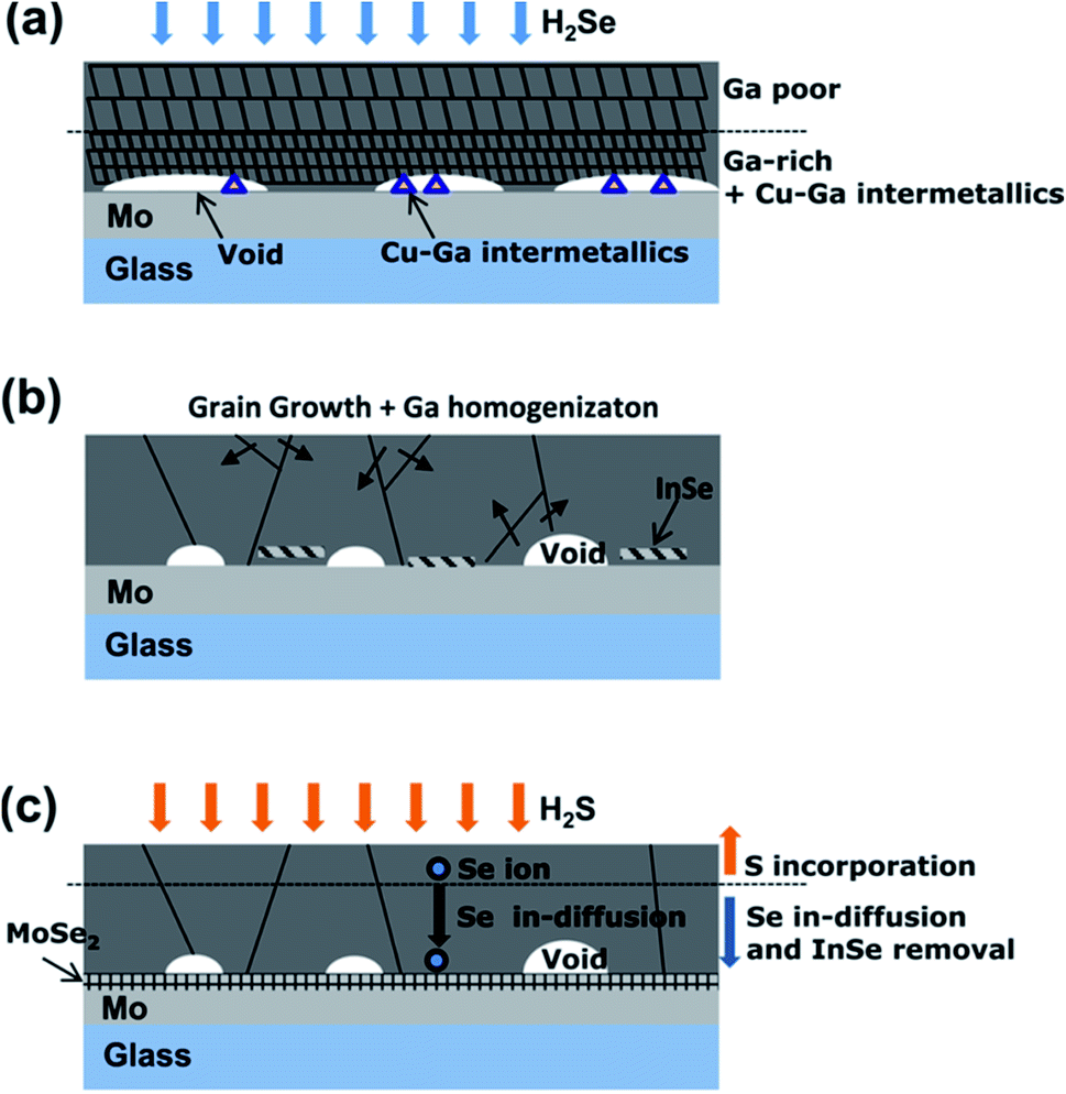 | ||
| Fig. 5 Growth model for the three-step reaction. (a) 1st step: due to the preferential reaction of In–Se, the surface region contains CIGSe with little Ga, while the back side has a higher Ga content with the Cu9Ga4 intermetallic compound with a finer microstructure; (b) 2nd step: recrystallization and Ga homogenization occur to reduce the surface energy as the Cu9Ga4 is incorporated into the CIGSe and InSe is formed; (c) 3rd step: S incorporation occurs near the film surface and stimulates Se in-diffusion toward the Mo back contact, leading to the consumption of InSe and the formation of MoSe2.49 Copyright 2012 American Institute of Physics. | ||
Ga homogenization should proceed in an inert atmosphere rather than under reactive Se or S vapor conditions because the interdiffusion of Ga and In is thought to occur along VSe, which can be more easily formed by annealing in an inert gas, while annealing in Se or S, or both, vapor inhibits the formation of VSe.69 For example, multiphase CIGSe film consisting of a CuInSe2 and CuGaSe2 phase could be converted to single phase CIGSe by annealing at 600 °C in an Ar atmosphere, while annealing in H2Se atmosphere still maintained the multiphase CIGSe film. On the other hand, the presence of Na also affects the diffusion of In and Ga since Na is known to passivate vacancy sites, like VSe. Besides the vacancy sites, flux agents can also influence the interdiffusion of In and Ga. The diffusion of In and Ga is higher under Cu-rich conditions, presumably due to the formation of flux agents, like Cu2−xSe.100 The Cu2−xSe flux agent was reported to enhance the out-diffusion of In and Ga from the CuInSe2 and CuGaSe2 phase, respectively.34,35 The higher diffusion under Cu-rich conditions also suggested that Cu vacancy sites do not favor In and Ga diffusion.
In the first-stage selenization proceeding at low temperature, In can be present in the form of the chalcopyrite CuInSe2 phase, whereas Ga in the chalcopyrite phase is not present since the formation temperature of CuGaSe2 is relatively higher than that of CuInSe2. For example, Han et al. showed that the formation temperature of CuGaSe2 is above 410 °C, whereas the formation temperature of CuInSe2 is between 340 °C and 380 °C.35 Ga remained in the form of Cu9Ga4 near the Mo back contact during the first-stage selenization step.49,101 The following Ar annealing step at 550 °C provided a diffusion route for Ga ions to the CuInSe2 chalcopyrite phase, followed by recrystallization with Ga since the Cu9Ga4 binary phase exists in a liquid and solid mixture phase above 485 °C. Kim et al. reported that, after the second air annealing step, a conductive InSe binary phase, which induces shunt generation, is formed; therefore a third and final selenization (or sulfurization) step is required to remove the InSe binary phase. After the third chalcogenization step, the solar cell efficiency was 14.2%, a value that is significantly higher than the efficiencies measured immediately after the first selenization step (0.9%) and the second inert gas annealing step (0.1%), thus demonstrating the importance of InSe phase removal (Fig. 6). On the other hand, the formation of InSe seems to be affected by the Cu content of the precursor layer. In the case of Cu-poor conditions, a high efficiency of 15.1% was obtained without the third chalcogenization step process.101
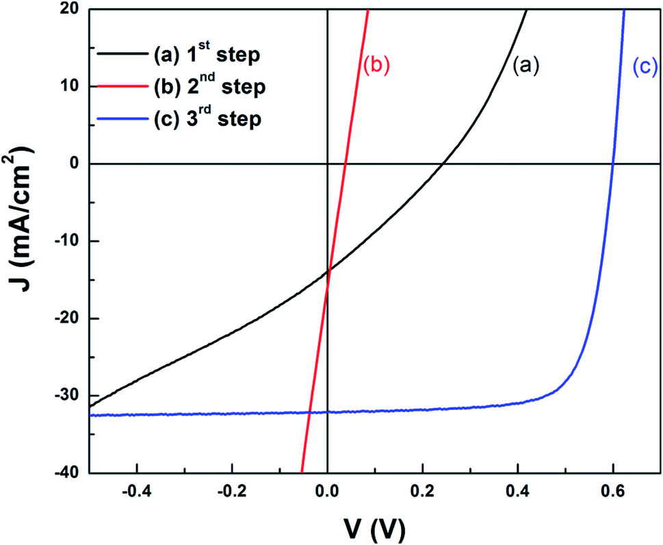 | ||
| Fig. 6 Light J–V curves of devices with the reacted CIGS or CIGSS films after: (a) 1st step, (b) 2nd step, and (c) 3rd step.49 Copyright 2012 American Institute of Physics. | ||
Post-selenization
As mentioned above, the sequential process often results in solar cells with a low Voc due to Ga segregation. Post-sulfurization is proving to be a pragmatic way to increase Voc but is already being used in commercialized modules by companies such as Solar Frontier.102,103 Post-sulfurization is commonly performed by annealing the CIGSe film in a H2S gas atmosphere, either by dipping the CIGSe film in a solution containing sulfur or by evaporating sulfur onto the CIGSe film.104,105 During post-sulfurization, S substitutes Se and increases the bandgap of the CIGSe film according to the following equation:106| Eg(x, y) = (1.00 + 0.13x2 + 0.08x2y + 0.13xy + 0.55x + 0.54y) eV | (7) |
 | ||
| Fig. 7 Schematic representation of the post-sulfurization. (a) Sulfurization of Ga accumulated CIGSe film. (b) Schematic band diagram of the sulfurized CIGSe films. | ||
As described in the “Theoretical background” section, the minimum bandgap of the absorber determines Jsc. Therefore, it is important that the post-sulfurization selectively enhances the bandgap near the surface of the CIGSe film to increase the Voc while maintaining the Jsc. Since S atoms are expected to diffuse through the grain boundary from the surface of the CIGSe film, the S diffusion depth becomes more shallow as the grain size and crystallinity of the CIGSe film increase.107 The S diffusion depth (i.e., the depth at which the gradual S substitution of Se occurs) increases with increasing the post-sulfurization temperature and time.102,107–109 It should be noted that the Ga incorporated in the CIGSe film also affects the incorporation of S since S preferentially reacts with Ga while Se preferentially reacts with In.50 Both the Ga content near the surface and Ga content in the entire CIGSe film affect S incorporation.110 While Ga promotes S incorporation, the post-sulfurization causes Ga to diffuse to the surface.50,107
Generally, in order to obtain high efficiency CIGSe solar cells, increasing the bandgap toward the surface (front grading) to achieve a higher Voc is required.26 In a typical 3-stage co-evaporation process, front grading is achieved by increasing the Ga content.10,28 However, the increase in Ga content only increases CBM and has little effect on VBM because CBM is determined by antibonding between the s orbital of the group III ion and the 4p orbital of the group VI ion.38,111,112 However, increasing the CBM at the surface can deteriorate the solar cell efficiency since it can act as a barrier to photogenerated electrons, especially under forward bias voltage, which reduces the SCR width significantly.28 In addition, a too high CBM in CIGSe films would form a “cliff”-like conduction band offset with a buffer layer, which would also deteriorate the solar cell performance because of the occurrence of recombination between the CBM of the buffer layer and the VBM of the absorber film.113 Fortunately, surface sulfurization carries beneficial effects without the need for a tradeoff since the formation of the barrier is derived from an excessive increase of the front side CBM. Surface sulfurization not only increases the CBM but also lowers the VBM, as the VBM is determined by antibonding between the Cu 3d orbital and the p orbital of the group VI ion.114 In addition, the lowering of the VBM at the surface layer repels the photogenerated holes away from the buffer/absorber interface to prevent e−–h+ recombination at the interface, resulting in a higher Voc. The recombination barrier height between the Fermi level and VBM also increases.115 When Kobayashi et al. investigated the effect of post-sulfurization on the CIGSe absorber fabricated by the co-evaporation process, the surface VBM of the CIGSe absorber without the post-sulfurization process was approximately 0.2 eV lower than that of bulk region, attributed to the Cu-poor phase and the post-sulfurization process, which further reduced the VBM by approximately 0.1 eV.116 After the post-sulfurization, the solar cell efficiency was increased from 15.1% to 17.3%, mainly due to the increase in Voc from 0.590 V to 0.674 V. It should be noted that Jsc exhibited a slight increase in value from 36.5 mA cm−2 to 37.1 mA cm−2, even though the bandgap vicinity at the surface increased. A beneficial effect of the lowering VBM was also demonstrated in a simulation.117 Three kinds of interface consisting of no interface defects, donor-like interface defects, and acceptor-like interface defects were considered. Surface sulfurization increased the solar cell efficiency in all cases. The efficiency improvement effect was not significant in the case of the no interface defects (19.35% vs. 19.8%) and donor-like interface defect (19.1% vs. 19.7%). However in the case of acceptor-like interface defects, the efficiency improvement effect was remarkable (16.1% vs. 19.3%), implying that the expected detrimental effect could be considerably prevented by the surface S incorporation.
Post-sulfurization is thought to passivate the defect, which further increases the Voc. Both deep-level and shallow-level defects can be passivated by post-sulfurization. For example, Rau et al. showed the passivation of deep-trap states by incorporating S into the CIGSe absorber.118 The activation energies (Ea) of the saturation currents in the CIGSe solar cells without and with S incorporation were 540 and 940 meV, respectively. The Ea and the energetic distance of the trap state (ET) closest to either VBM or CBM followed the equation:
| Ea = EG − ET | (8) |
The S atoms substitute the Se atoms during the post-sulfurization.107 Therefore, the post-sulfurization process can cause the regrowth of films despite the absence of additional Se, because the substituted Se atoms supplied to the film itself diffuses inward. This regrowth may increase the grain size of the CIGSe film. An increase in quantum efficiency in the short wavelength region was observed along with this phenomenon, which was probably related to the improved crystallinity and size of the grains. The regrowth also reduces the thickness of the fine grain layer formed at the bottom in the sequential process.102 The substituted Se atoms can also improve the electrical properties of the Mo/CIGSe interface by reacting the Mo substrate with the diffused Se to form MoSe2 which is known to form a quasi-ohmic contact and to have a positive effect on the efficiency.49,57
Still, however, excessive post-sulfurization degrades the efficiency of solar cells. The post-sulfurization in overly long time periods reduces the grain size of the CIGSe film since CuInGaS2 generally has a smaller grain size than CuInGaSe2.109 The solar cell subjected to 40 min sulfurization exhibited a poorer efficiency than that subjected to 20 min sulfurization. The worsening of the efficiency was mainly attributed to the decrease in Jsc and FF, presumably owing to their reduced grain sizes. In addition, long durations or high temperatures in the post-sulfurization process also increases the thickness of the bottom fine grain layer.102 The formation of the conductive Cu(S,Se)2 phase is also one of the causes of lowering the FF.11 However, the Voc is increased as the degree of sulfurization increases by increasing the sulfurization time or temperature, or both. Although the harsh post-sulfurization condition results in a lower FF, S incorporation increases the FF within a specific region in the range of 0 ≤ S/(Se + S) ≤ 0.3. Excess sulfurization also induces too high a front bandgap gradient, which deteriorates the carrier collection and reduces the FF.110
Summary and outlook
The two-step sequential fabrication process is an attractive method since it is expected to fabricate CIGSe absorbers at a more reasonable cost than possible with the co-evaporation fabrication process. However, the lower Voc attributed to the accumulation of Ga the toward bottom during the chalcogenization process should be solved to achieve high efficiency through the two-step sequential process. To overcome this issue, three categories of efficiency improvement strategies, namely pre-selenization, mid-selenization, and post-selenization have been proposed. Pre-selenization strategies mainly focus on the adjustment of the metal precursor layer, where the main strategy is to suppress the diffusion of Ga to the bottom side or intentionally to raise the Ga content near the absorber surface. Pre-selenization strategies are divided into two categories, namely the vacuum process and the solution process. The vacuum process is expected to be free of impurities and so able to produce high-quality metal precursor layers, but it is an inconvenient process still due to the need for high-costing vacuum equipment. During selenization strategies, focus must be placed on the inert gas annealing process to diffuse segregated Ga toward the surface. After the selenization strategies focus on the post-sulfurization process to compensate for the deficiency of Ga with S, which play a similar role to Ga, i.e., front bandgap grading. Strategies of different categories can be applied together in one absorber manufacturing process because of the different application times. Although the certified world record in CIGSe solar cells produced by the one-pot 3-stage co-evaporation process is 22.6%, the record efficiency of the sequential fabrication process is almost similar (22.3%).12 A promising submodule (30 cm × 30 cm) efficiency of 19.2% has already been announced by Solar Frontier, which show a promising path for this technology.Future technology development of the sequential process is expected to be meaningful, not only in terms of efficiency increases but also in cost reduction. Shortening the process time is expected to have a significant impact on cost reduction. Recently, a 15.5% efficiency was achieved with only a few minutes of selenization by a rapid thermal processing (RTP).44 The application of the RTP process is meaningful not only in reducing the process time, but also in minimizing the thermal energy usage. On the other hand, the one-pot 3-stage co-evaporation process has limitations in reducing the commercial losses caused by the process time and usage of thermal energy due to the slow deposition of In and Ga.121 In addition, the post-sulfurization process may be shortened by the simultaneous selenization and sulfurization. The resulting solar cell from S simultaneous selenization and sulfurization with Se vapor and H2S gas achieved 11.7% efficiency without ARC and 12.3% with ARC even when using the solution process.94 Recently, the same research group achieved an efficiency of 14.3% using the solution process by introducing an inert gas annealing process and a ternary buffer layer in the simultaneous selenization and sulfurization process even without ARC.122 On the other hand, in terms of efficiency, further improvements are expected to be achieved through alkali metal incorporation. The incorporation of Na and K has already been demonstrated by Solar Frontier.123 Additional efficiency improvements are expected in the near future with the incorporation of heavy alkali metals, such as Rb and Cs.4
Conflicts of interest
There are no conflicts to declare.Abbreviations
| CIGSe | Cu(In,Ga)Se2 |
| J sc | Short circuit current density |
| V oc | Open circuit potential |
| ARC | Anti reflection coating |
| SCR | Space charge region |
| FF | Fill factor |
| CBM | Conduction band minimum |
| VBM | Valence band maximum |
Acknowledgements
This work was supported by the Energy Technology Development Program of the Korea Institute of Energy Technology Evaluation and Planning (KETEP) grant (20163010012570) and the program of the Korea Institute of Science and Technology (KIST).References
- T. D. Lee and A. U. Ebong, Renewable Sustainable Energy Rev., 2017, 70, 1286–1297 CrossRef.
- J. Ramanujam and U. P. Singh, Energy Environ. Sci., 2017, 10, 1306–1319 RSC.
- L. L. Kazmerski, F. R. White and G. K. Morgan, Appl. Phys. Lett., 1976, 29, 268–270 CrossRef.
- P. Jackson, R. Wuerz, D. Hariskos, E. Lotter, W. Witte and M. Powalla, Phys. Status Solidi RRL, 2016, 10, 583–586 CrossRef.
- E. Jarzembowski, M. Maiberg, F. Obereigner, K. Kaufmann, S. Krause and R. Scheer, Thin Solid Films, 2015, 576, 75–80 CrossRef.
- J. F. Guillemoles, Thin Solid Films, 2002, 403–404, 405–409 CrossRef.
- U. P. Singh and S. P. Patra, Int. J. Photoenergy, 2010, 2010, 1–19 CrossRef.
- A. R. Uhl, P. Fuchs, A. Rieger, F. Pianezzi, C. M. Sutter-Fella, L. Kranz, D. Keller, H. Hagendorfer, Y. E. Romanyuk, F. LaMattina, S. Yoon, L. Karvonen, T. Magorian-Friedlmeier, E. Ahlswede, D. VanGenechten, F. Stassin and A. N. Tiwari, Prog. Photovoltaics, 2015, 23, 1110–1119 Search PubMed.
- Y. E. Romanyuk, H. Hagendorfer, P. Stücheli, P. Fuchs, A. R. Uhl, C. M. Sutter-Fella, M. Werner, S. Haass, J. Stückelberger, C. Broussillou, P.-P. Grand, V. Bermudez and A. N. Tiwari, Adv. Funct. Mater., 2015, 25, 12–27 CrossRef.
- T. Feurer, P. Reinhard, E. Avancini, B. Bissig, J. Löckinger, P. Fuchs, R. Carron, T. P. Weiss, J. Perrenoud, S. Stutterheim, S. Buecheler and A. N. Tiwari, Prog. Photovoltaics, 2017, 25, 645–667 Search PubMed.
- S. Niki, M. Contreras, I. Repins, M. Powalla, K. Kushiya, S. Ishizuka and K. Matsubara, Prog. Photovoltaics, 2010, 18, 453–466 Search PubMed.
- R. Kamada, T. Yagioka, S. Adachi, A. Handa, K. F. Tai, T. Kato and H. Sugimoto, in Photovoltaic Specialist Conference (PVSC), 2016 IEEE 43rd, 2016, pp. 1287–1291 Search PubMed.
- J. Nam, Y. Kang, D. Lee, J. Yang, Y.-S. Kim, C. B. Mo, S. Park and D. Kim, Prog. Photovoltaics, 2016, 24, 175–182 Search PubMed.
- C. Broussillou, C. Viscogliosi, A. Rogee, S. Angle, P. P. Grand, S. Bodnar, C. Debauche, J. L. Allary, B. Bertrand, C. Guillou, L. Parissi and S. Coletti, in Photovoltaic Specialist Conference (PVSC), 2015 IEEE 42nd, 2015, pp. 1–5 Search PubMed.
- A. Chirilă, P. Reinhard, F. Pianezzi, P. Bloesch, A. R. Uhl, C. Fella, L. Kranz, D. Keller, C. Gretener, H. Hagendorfer, D. Jaeger, R. Erni, S. Nishiwaki, S. Buecheler and A. N. Tiwari, Nat. Mater., 2013, 12, 1107 CrossRef PubMed.
- P. Jackson, D. Hariskos, E. Lotter, S. Paetel, R. Wuerz, R. Menner, W. Wischmann and M. Powalla, Prog. Photovoltaics, 2011, 19, 894–897 Search PubMed.
- P. Jackson, D. Hariskos, R. Wuerz, W. Wischmann and M. Powalla, Phys. Status Solidi RRL, 2014, 8, 219–222 CrossRef.
- P. Jackson, D. Hariskos, R. Wuerz, O. Kiowski, A. Bauer, T. M. Friedlmeier and M. Powalla, Phys. Status Solidi RRL, 2015, 9, 28–31 CrossRef.
- S.-H. Wei, S. B. Zhang and A. Zunger, Appl. Phys. Lett., 1998, 72, 3199–3201 CrossRef.
- X. Fontané, V. Izquierdo-Roca, L. Calvo-Barrio, A. Pérez-Rodríguez, J. R. Morante, D. Guettler, A. Eicke and A. N. Tiwari, Appl. Phys. Lett., 2009, 95, 261912 CrossRef.
- U. Rau and H. W. Schock, Appl. Phys. A, 1999, 69, 131–147 CrossRef.
- K. W. Mitchel and H. I. Liu, in Photovoltaic specialists conference, 1988, conference record of the twentieth IEEE, IEEE, 1988 Search PubMed.
- H. K. Song, J. K. Jeong, H. J. Kim, S. K. Kim and K. H. Yoon, Thin Solid Films, 2003, 435, 186–192 CrossRef.
- T. Nakabayashi, T. Miyazawa, Y. Hashimoto and K. Ito, Sol. Energy Mater. Sol. Cells, 1997, 49, 375–381 CrossRef.
- J.-P. Bäcker, S. S. Schmidt, H. Rodriguez-Alvarez, C. Wolf, C. A. Kaufmann, M. Hartig, R. Mainz and R. Schlatmann, Sol. Energy Mater. Sol. Cells, 2017, 162, 120–126 CrossRef.
- T. Dullweber, U. Rau, M. A. Contreras, R. Noufi and H. W. Schock, IEEE Trans. Electron Devices, 2000, 47, 2249–2254 CrossRef.
- M. Topič, F. Smole and J. Furlan, J. Appl. Phys., 1996, 79, 8537–8540 CrossRef.
- A. Chirilă, S. Buecheler, F. Pianezzi, P. Bloesch, C. Gretener, A. R. Uhl, C. Fella, L. Kranz, J. Perrenoud, S. Seyrling, R. Verma, S. Nishiwaki, Y. E. Romanyuk, G. Bilger and A. N. Tiwari, Nat. Mater., 2011, 10, 857 CrossRef PubMed.
- A. Niemegeers, M. Burgelman and A. D. Vos, Appl. Phys. Lett., 1995, 67, 843–845 CrossRef.
- R. Klenk, Thin Solid Films, 2001, 387, 135–140 CrossRef.
- T. Minemoto, T. Matsui, H. Takakura, Y. Hamakawa, T. Negami, Y. Hashimoto, T. Uenoyama and M. Kitagawa, Sol. Energy Mater. Sol. Cells, 2001, 67, 83–88 CrossRef.
- R. Scheer, Prog. Photovoltaics, 2012, 20, 507–511 Search PubMed.
- Y.-C. Wang and H.-P. D. Shieh, Appl. Phys. Lett., 2013, 103, 153502 CrossRef.
- M. Marudachalam, R. W. Birkmire, H. Hichri, J. M. Schultz, A. Swartzlander and M. M. Al-Jassim, J. Appl. Phys., 1997, 82, 2896–2905 CrossRef.
- J. Han, C. Liao, T. Jiang, H. Xie, K. Zhao and M. P. Besland, J. Cryst. Growth, 2013, 382, 56–60 CrossRef.
- F. Hergert, S. Jost, R. Hock, M. Purwins and J. Palm, Thin Solid Films, 2007, 515, 5843–5847 CrossRef.
- R. Caballero, C. Guillén, M. T. Gutiérrez and C. A. Kaufmann, Prog. Photovoltaics, 2006, 14, 145–153 Search PubMed.
- S. H. Wei and A. Zunger, J. Appl. Phys., 1995, 78, 3846–3856 CrossRef.
- O. Lundberg, M. Edoff and L. Stolt, Thin Solid Films, 2005, 480–481, 520–525 CrossRef.
- J. Chantana, D. Hironiwa, T. Watanabe, S. Teraji, K. Kawamura and T. Minemoto, Sol. Energy Mater. Sol. Cells, 2015, 133, 223–228 CrossRef.
- M. A. Contreras, J. Tuttle, A. Gabor, A. Tennant, K. Ramanathan, S. Asher, A. Franz, J. Keane, L. Wang and R. Noufi, Sol. Energy Mater. Sol. Cells, 1996, 41–42, 231–246 CrossRef.
- H. K. Song, S. G. Kim, H. J. Kim, S. K. Kim, K. W. Kang, J. C. Lee and K. H. Yoon, Sol. Energy Mater. Sol. Cells, 2003, 75, 145–153 CrossRef.
- H. Park, S. C. Kim, S.-H. Lee, J. Koo, S. H. Lee, C.-W. Jeon, S. Yoon and W. K. Kim, Thin Solid Films, 2011, 519, 7245–7249 CrossRef.
- S. S. Schmidt, C. Wolf, H. Rodriguez-Alvarez, J.-P. Bäcker, C. A. Kaufmann, S. Merdes, F. Ziem, M. Hartig, S. Cinque, I. Dorbandt, C. Köble, D. Abou-Ras, R. Mainz and R. Schlatmann, Prog. Photovoltaics, 2017, 25, 341–357 Search PubMed.
- T.-T. Wu, J.-H. Huang, F. Hu, C.-h. Chang, W.-L. Liu, T.-H. Wang, C.-H. Shen, J.-M. Shieh and Y.-L. Chueh, Nano Energy, 2014, 10, 28–36 CrossRef.
- G. S. Chen, J. C. Yang, Y. C. Chan, L. C. Yang and W. Huang, Sol. Energy Mater. Sol. Cells, 2009, 93, 1351–1355 CrossRef.
- J. Tong, H. Zeng, Q.-M. Song, Z.-A. Xu and C.-L. Yang, Sol. Energy Mater. Sol. Cells, 2016, 150, 88–94 CrossRef.
- M. Purwins, R. Enderle, M. Schmid, P. Berwian, G. Müller, F. Hergert, S. Jost and R. Hock, Thin Solid Films, 2007, 515, 5895–5898 CrossRef.
- K. Kim, G. M. Hanket, T. Huynh and W. N. Shafarman, J. Appl. Phys., 2012, 111, 083710 CrossRef.
- G. M. Hanket, W. N. Shafarman, B. E. McCandless and R. W. Birkmire, J. Appl. Phys., 2007, 102, 074922 CrossRef.
- C. P. Muzzillo, C. E. Campbell and T. J. Anderson, J. Mater. Sci., 2016, 51, 3362–3379 CrossRef.
- S. Luo, J.-H. Lee, C.-W. Liu, J.-M. Shieh, C.-H. Shen, T.-T. Wu, D. Jang and J. R. Greer, Appl. Phys. Lett., 2014, 105, 011907 CrossRef.
- A. Gupta and S. Isomura, Sol. Energy Mater. Sol. Cells, 1998, 53, 385–401 CrossRef.
- Y. Tauchi, K. Kim, H. Park and W. Shafarman, IEEE Journal of Photovoltaics, 2013, 3, 467–471 Search PubMed.
- S. Soltanmohammad, L. Chen, B. McCandless and W. N. Shafarman, IEEE Journal of Photovoltaics, 2017, 7, 273–280 Search PubMed.
- N. Kohara, S. Nishiwaki, Y. Hashimoto, T. Negami and T. Wada, Sol. Energy Mater. Sol. Cells, 2001, 67, 209–215 CrossRef.
- K.-J. Hsiao, J.-D. Liu, H.-H. Hsieh and T.-S. Jiang, Phys. Chem. Chem. Phys., 2013, 15, 18174–18178 RSC.
- R. Usui, T. Tomizawa, T. Okato and H. Odaka, Conference Record of the 38th IEEE Photovoltaic Specialists Conference (PVSC) 2012, pp. 3109–3111 Search PubMed.
- W. Takahiro, K. Naoki, N. Takayuki and N. Mikihiko, Jpn. J. Appl. Phys., 1996, 35, L1253 CrossRef.
- D. Abou-Ras, G. Kostorz, D. Bremaud, M. Kälin, F. V. Kurdesau, A. N. Tiwari and M. Döbeli, Thin Solid Films, 2005, 480–481, 433–438 CrossRef.
- T. Klinkert, B. Theys, G. Patriarche, M. Jubault, F. Donsanti, J.-F. Guillemoles and D. Lincot, J. Chem. Phys., 2016, 145, 154702 CrossRef PubMed.
- T. Wada, N. Kohara, S. Nishiwaki and T. Negami, Thin Solid Films, 2001, 387, 118–122 CrossRef.
- K. Kim, H. Park, G. M. Hanket, W. K. Kim and W. N. Shafarman, Prog. Photovoltaics, 2015, 23, 765–772 Search PubMed.
- K.-H. Liao, C.-Y. Su and Y.-T. Ding, J. Alloys Compd., 2013, 581, 250–256 CrossRef.
- R. Mainz, A. Weber, H. Rodriguez-Alvarez, S. Levcenko, M. Klaus, P. Pistor, R. Klenk and H.-W. Schock, Prog. Photovoltaics, 2015, 23, 1131–1143 Search PubMed.
- W. Liu, Y. Sun, W. Li, C.-J. Li, F.-Y. Li and J.-G. Tian, Appl. Phys. A, 2007, 88, 653–656 CrossRef.
- Y.-C. Wang and H.-P. D. Shieh, Appl. Phys. Lett., 2014, 105, 073901 CrossRef.
- H. R. Hsu, S. C. Hsu and Y.-s. Liu, Appl. Phys. Lett., 2012, 100, 233903 CrossRef.
- M. Marudachalam, H. Hichri, R. Klenk, R. W. Birkmire, W. N. Shafarman and J. M. Schultz, Appl. Phys. Lett., 1995, 67, 3978–3980 CrossRef.
- S.-K. Lee, J.-K. Sim, N. J. S. Kissinger, I.-S. Song, J.-S. Kim, B.-J. Baek and C.-R. Lee, J. Alloys Compd., 2015, 633, 31–36 CrossRef.
- M. S. Park, S.-J. Sung and D.-H. Kim, J. Nanosci. Nanotechnol., 2015, 15, 2490–2494 CrossRef PubMed.
- S.-Y. Hsiao, P.-C. Yang, H.-C. Ni, K.-Y. Yen, C.-H. Chiu, P.-S. Lin, H.-J. Chen, C.-H. Wu, S.-C. Liang, G.-Y. Ni, F.-W. Jih, C.-D. Chiang and J.-R. Gong, J. Electrochem. Soc., 2012, 159, H378–H383 CrossRef.
- S. Tomoaki, K. Yoshifumi, S. Mutsumi and F. C. Shigefusa, Jpn. J. Appl. Phys., 2011, 50, 05FB05 CrossRef.
- L. Guangmin, L. Wei, L. Yiming, L. Shuping, L. Xiaodong, Z. Yi, Z. Zhiqiang, H. Qing and S. Yun, Semicond. Sci. Technol., 2015, 30, 105012 CrossRef.
- S.-M. Youn, J.-H. Kim and C. Jeong, J. Nanosci. Nanotechnol., 2016, 16, 5003–5007 CrossRef PubMed.
- P. Schöppe, C. S. Schnohr, M. Oertel, A. Kusch, A. Johannes, S. Eckner, M. Burghammer, G. Martínez-Criado, U. Reislöhner and C. Ronning, Appl. Phys. Lett., 2015, 106, 013909 CrossRef.
- C.-H. Wu, F.-S. Chen, S.-H. Lin and C.-H. Lu, Ceram. Int., 2013, 39, 3393–3397 CrossRef.
- J. Haarstrich, H. Metzner, M. Oertel, C. Ronning, T. Rissom, C. A. Kaufmann, T. Unold, H. W. Schock, J. Windeln, W. Mannstadt and E. Rudigier-Voigt, Sol. Energy Mater. Sol. Cells, 2011, 95, 1028–1030 CrossRef.
- C. J. Hibberd, E. Chassaing, W. Liu, D. B. Mitzi, D. Lincot and A. N. Tiwari, Prog. Photovoltaics, 2010, 18, 434–452 Search PubMed.
- H. Azimi, Y. Hou and C. J. Brabec, Energy Environ. Sci., 2014, 7, 1829–1849 RSC.
- D. Lee and K. Yong, Korean J. Chem. Eng., 2013, 30, 1347–1358 CrossRef.
- T. Zhang, Y. Yang, D. Liu, S. C. Tse, W. Cao, Z. Feng, S. Chen and L. Qian, Energy Environ. Sci., 2016, 9, 3674–3681 RSC.
- M. Kaelin, D. Rudmann, F. Kurdesau, H. Zogg, T. Meyer and A. N. Tiwari, Thin Solid Films, 2005, 480–481, 486–490 CrossRef.
- S. Ahn, C. Kim, J. H. Yun, J. Gwak, S. Jeong, B.-H. Ryu and K. Yoon, J. Phys. Chem. C, 2010, 114, 8108–8113 CrossRef.
- S.-N. Park, S.-J. Sung, D.-H. Son, D.-H. Kim, M. Gansukh, H. Cheong and J.-K. Kang, RSC Adv., 2014, 4, 9118–9125 RSC.
- S. J. Park, J. W. Cho, J. K. Lee, K. Shin, J.-H. Kim and B. K. Min, Prog. Photovoltaics, 2014, 22, 122–128 Search PubMed.
- E. Lee, S. J. Park, J. W. Cho, J. Gwak, M.-K. Oh and B. K. Min, Sol. Energy Mater. Sol. Cells, 2011, 95, 2928–2932 CrossRef.
- R. Mainz, B. C. Walker, S. S. Schmidt, O. Zander, A. Weber, H. Rodriguez-Alvarez, J. Just, M. Klaus, R. Agrawal and T. Unold, Phys. Chem. Chem. Phys., 2013, 15, 18281–18289 RSC.
- S. Rehan, K. Y. Kim, J. Han, Y.-J. Eo, J. Gwak, S. K. Ahn, J. H. Yun, K. Yoon, A. Cho and S. Ahn, ACS Appl. Mater. Interfaces, 2016, 8, 5261–5272 CrossRef PubMed.
- V. Haug, A. Quintilla, I. Klugius and E. Ahlswede, Thin Solid Films, 2011, 519, 7464–7467 CrossRef.
- T. K. Todorov, O. Gunawan, T. Gokmen and D. B. Mitzi, Prog. Photovoltaics, 2013, 21, 82–87 Search PubMed.
- B. Bob, B. Lei, C.-H. Chung, W. Yang, W.-C. Hsu, H.-S. Duan, W. W.-J. Hou, S.-H. Li and Y. Yang, Adv. Energy Mater., 2012, 2, 504–522 CrossRef.
- D. B. Mitzi, M. Yuan, W. Liu, A. J. Kellock, S. J. Chey, V. Deline and A. G. Schrott, Adv. Mater., 2008, 20, 3657–3662 CrossRef.
- S. J. Park, H. S. Jeon, J. W. Cho, Y. J. Hwang, K. S. Park, H. S. Shim, J. K. Song, Y. Cho, D.-W. Kim, J. Kim and B. K. Min, ACS Appl. Mater. Interfaces, 2015, 7, 27391–27396 CrossRef PubMed.
- S. J. Park, H. S. An, J. E. Kim, H. S. Jeon, S. S. Yoon, Y. J. Hwang, J. Kim, D.-W. Kim and B. K. Min, RSC Adv., 2015, 5, 103439–103444 RSC.
- H. S. An, Y. Cho, S. J. Park, H. S. Jeon, Y. J. Hwang, D.-W. Kim and B. K. Min, ACS Appl. Mater. Interfaces, 2014, 6, 888–893 CrossRef PubMed.
- S. H. Sohn, N. S. Han, Y. J. Park, S. M. Park, H. S. An, D.-W. Kim, B. K. Min and J. K. Song, Phys. Chem. Chem. Phys., 2014, 16, 27112–27118 RSC.
- S. Jeong, S. H. Sohn, H. S. Shim, S. M. Park, B. K. Min and J. K. Song, Bull. Korean Chem. Soc., 2016, 37, 91–94 CrossRef.
- J. Bi, J. Ao, M.-J. Jeng, L. Yao, S. Gao, G. Sun, Q. He, Z. Zhou, Y. Sun, Y.-L. Xiao and L.-B. Chang, Sol. Energy Mater. Sol. Cells, 2017, 159, 352–361 CrossRef.
- O. Lundberg, J. Lu, A. Rockett, M. Edoff and L. Stolt, J. Phys. Chem. Solids, 2003, 64, 1499–1504 CrossRef.
- H. Anjun, H. Yongliang, L. Xiaohui, X. Wang, M. Fanying and L. Zhengxin, Jpn. J. Appl. Phys., 2016, 55, 115502 CrossRef.
- Y. Goushi, H. Hakuma, K. Tabuchi, S. Kijima and K. Kushiya, Sol. Energy Mater. Sol. Cells, 2009, 93, 1318–1320 CrossRef.
- K. Kushiya, Sol. Energy Mater. Sol. Cells, 2014, 122, 309–313 CrossRef.
- W. Li, S. R. Cohen and D. Cahen, Sol. Energy Mater. Sol. Cells, 2014, 120, 500–505 CrossRef.
- D. Ohashi, T. Nakada and A. Kunioka, Sol. Energy Mater. Sol. Cells, 2001, 67, 261–265 CrossRef.
- M. Bär, W. Bohne, J. Röhrich, E. Strub, S. Lindner, M. C. Lux-Steiner, C.-H. Fischer, T. P. Niesen and F. Karg, J. Appl. Phys., 2004, 96, 3857–3860 CrossRef.
- T. Nakada, H. Ohbo, T. Watanabe, H. Nakazawa, M. Matsui and A. Kunioka, Sol. Energy Mater. Sol. Cells, 1997, 49, 285–290 CrossRef.
- J. W. Jang, S. M. Lee, I. J. Choi and Y. S. Cho, J. Alloys Compd., 2017, 710, 177–181 CrossRef.
- S.-H. Lin, J.-C. Sung and C.-H. Lu, Thin Solid Films, 2016, 616, 746–753 CrossRef.
- C.-Y. Huang, W.-C. Lee and A. Lin, J. Appl. Phys., 2016, 120, 094502 CrossRef.
- T. Maeda, T. Takeichi and T. Wada, Phys. Status Solidi A, 2006, 203, 2634–2638 CrossRef.
- M. Turcu, I. M. Kötschau and U. Rau, J. Appl. Phys., 2002, 91, 1391–1399 CrossRef.
- K. Sun, C. Yan, F. Liu, J. Huang, F. Zhou, J. A. Stride, M. Green and X. Hao, Adv. Energy Mater., 2016, 6, 1600046 CrossRef.
- J. E. Jaffe and A. Zunger, Phys. Rev. B, 1984, 29, 1882–1906 CrossRef.
- T. Lavrenko, T. Ott and T. Walter, Thin Solid Films, 2015, 582, 51–55 CrossRef.
- T. Kobayashi, H. Yamaguchi, Z. Jehl Li Kao, H. Sugimoto, T. Kato, H. Hakuma and T. Nakada, Prog. Photovoltaics, 2015, 23, 1367–1374 Search PubMed.
- Z. Jehl Li Kao, T. Kobayashi and T. Nakada, Sol. Energy, 2014, 110, 50–55 CrossRef.
- U. Rau, M. Schmitt, F. Engelhardt, O. Seifert, J. Parisi, W. Riedl, J. Rimmasch and F. Karg, Solid State Commun., 1998, 107, 59–63 CrossRef.
- F.-S. Chen, J.-S. Ma, J.-C. Sung and C.-H. Lu, Sol. Energy Mater. Sol. Cells, 2014, 124, 166–171 CrossRef.
- R. Knecht, M. S. Hammer, J. Parisi and I. Riedel, Phys. Status Solidi A, 2013, 210, 1392–1399 CrossRef.
- A. Chirilă, S. Seyrling, S. Buecheler, D. Guettler, S. Nishiwaki, Y. E. Romanyuk, G. Bilger and A. N. Tiwari, Prog. Photovoltaics, 2012, 20, 209–216 Search PubMed.
- G. S. Park, V. B. Chu, B. W. Kim, D.-W. Kim, H.-S. Oh, Y. J. Hwang and B. K. Min, ACS Appl. Mater. Interfaces, 2018, 10, 9894–9899 CrossRef PubMed.
- P. M. P. Salomé, H. Rodriguez-Alvarez and S. Sadewasser, Sol. Energy Mater. Sol. Cells, 2015, 143, 9–20 CrossRef.
| This journal is © The Royal Society of Chemistry 2018 |