
Design of a novel and highly stable lead-free Cs2NaBiI6 double perovskite for photovoltaic application†
Chu
Zhang
 a,
Liguo
Gao
b,
Siowhwa
Teo
a,
Zhanglin
Guo
a,
Zhenhua
Xu
a,
Shuai
Zhao
c and
Tingli
Ma
*a
a,
Liguo
Gao
b,
Siowhwa
Teo
a,
Zhanglin
Guo
a,
Zhenhua
Xu
a,
Shuai
Zhao
c and
Tingli
Ma
*a
aGraduate School of Life Science and Systems Engineering, Kyushu Institute of Technology, Kitakyushu, Fukuoka 808-0196, Japan. E-mail: tinglima@life.kyutech.ac.jp
bSchool of Petroleum and Chemical Engineering, Dalian University of Technology, Panjin Campus, Panjin 124221, P. R. China
cSchool of Science, Chongqing University of Technology, Chongqing, 400054, P. R. China
First published on 24th May 2018
Abstract
In recent years, lead-based perovskites have become the most promising photovoltaic materials, showing excellent photoelectronic performance. However, the lead-based perovskites also exhibit instability and significant environmental impact. In this study, we have first reported the synthesis and characterization of a new lead-free double perovskite material, Cs2NaBiI6 (CNBI), and determined its crystal structure and optical properties by various testing methods. CNBI has a low band gap of 1.66 eV and exhibits high stability against moisture and oxygen in ambient air. We have also inspected the crystal growth process of CNBI and elucidated its crystal growth mechanism. Solar cell devices fabricated with CNBI as the absorber layer have shown great stability and reproducibility.
1. Introduction
The power conversion efficiency (PCE) of lead halide-based perovskite solar cells has increased to a high value of 22%1 owing to their wide absorption range,2 long electron and hole diffusion length,3 high quantum conversion ratio,4 low direct band gap, and defect tolerance ability.5 However, the stability and toxicity of lead-based perovskite photoactive materials are the main obstacles towards their commercialization due to irreversible decomposition caused by heat, moisture, and UV radiation.6,7 Relentless efforts have been made to counteract the stability issue by replacing the organic methylammonium cation with an inorganic cesium cation in the devices. To mitigate the toxicity issue of the current lead-based solar cells, lead metal is replaced by other more environmentally friendly elements such as tin, bismuth, germanium, copper, and alkaline-earth metals (Ba, Sr, and Ca).8–12 Research has been performed on tin (Sn)-based perovskite solar cells; however, Sn2+ ion is highly unstable and can be easily oxidized to Sn4+, which leads to decreased photovoltaic performance.Recently, bismuth-based perovskites have emerged as a promising choice to replace lead-based perovskites due to bismuth's non-toxic and stable 6p-block structure properties. In addition, computational predictions suggest that Bi-based perovskites exhibit lower intrinsic trap densities, fewer defect states, long carrier lifetimes, and defect-tolerant properties.13 Alternatively, engineering double perovskite materials by replacing divalent Pb2+ ions with monovalent B+ and trivalent B3+ ions in the form of A2B+B3+X6 (also denoted as elpasolite), which has a double perovskite structure, can be a strategy towards synthesizing stable and environmentally benign perovskites.14
To date, the most discussed double perovskite combination is that of Ag and Bi elements for the B sites. A complex and detailed computational analysis on the thermodynamic stability, electronic structure and defect properties of Cs2AgBiBr6 compound was conducted by Xiao et al.;15 they found that Cs2AgBiBr6 is less stable than CH3NH3PbBr3 due to weak coupling between Bi 6s and Br 6p orbitals in Cs2AgBiBr6.15 In addition, it was revealed that Cs2AgBiX6 has a corner-shared octahedral framework, which is similar to that of Pb-perovskite. Although this material exhibited excellent long PL decay time (indicating long carrier lifetime), the calculations and experimental data showed that Cs2AgBiX6 has a large indirect band gap of over 2 eV.16–20 Cheng et al. reported that a 2D hexagonal MA2AgBiI6 crystal possesses a wide band gap of 1.96 eV, which hinders its application in photovoltaic devices.21
Apart from Ag/Bi double perovskites, a Cs2InAgCl6 double perovskite was reported by Volonakis et al. in 2017.22 First-principle calculations predicted that Cs2InAgCl6 has a direct band gap, which is an advantage for photovoltaic applications. However, the band gap of this material is still very large (approaching 3 eV). Another double perovskite MA2KBiCl6 also exhibited a large bandgap of 3.04 eV despite its similar crystal structure to Pb-based perovskites.22,23 Notably, double perovskite materials listed above and reported elsewhere generally show high stability, which can reduce environmental impact.
The major disadvantage of the reported double perovskites is that their band gaps are all too large for use in single-junction solar cells. Hence, the design of a low band gap double perovskite halide is greatly needed; the new double perovskite should have an appropriate band gap with wide absorption range across the solar spectrum, and it should maintain the advantages of double perovskites such as stability and non-toxicity.
We herein present our study on the successful synthesis of highly crystalline, stable, and novel Cs2NaBiI6 (CNBI) lead-free double perovskite via a facile one-step hydrothermal process. CNBI double perovskite exhibits tolerance and octahedral factors of 0.849 and 0.466, respectively (ESI†). In this manuscript, we have provided an in-depth study on the CNBI crystal growth process under the influence of various acid concentrations and a plausible crystal growth mechanism. Our synthesized CNBI double perovskite possesses a band gap of 1.66 eV, excellent stability, and good light absorption performances, which fulfil the criteria for photovoltaic applications. It is worth noting that the CNBI double perovskite material is the first material to be synthesized and utilized in lab-scale solar cell applications with an efficiency of 0.42%, which is comparable to those of other lead-free perovskite solar cells.
2. Experimental
2.1 Synthesis of the target compound
The target double perovskite material was synthesized by a simple one-step hydrothermal process. Cesium iodide (99.999% trace metals basis, Sigma-Aldrich), sodium iodide (99.999% trace metals basis, Sigma-Aldrich) and bismuth iodide (99.999% trace metals basis, Sigma-Aldrich) were dissolved in 12 mL of 9 M hydroiodic acid (47 wt% in water, stored in refrigerator, Sigma-Aldrich) at a stoichiometric molar ratio. After a short period of magnetic stirring, the solution was transferred to an autoclave. The hydrothermal reaction was carried out at 120 °C for 2 h and then, the solution was slowly cooled to room temperature over 12 h to obtain sand-like, dark cerise crystals of the target material. The as-synthesized crystals were washed with D.I. water, centrifuged multiple times until the supernatant was colourless, and then dried in a vacuum chamber to obtain the final product.2.2 Characterization of CNBI
XRD (Rigaku XRD-DSC-XII) and XPS (ThermoFisher ESCALAB™ 250Xi) tests were carried out in the range of 5° to 80° (5° min−1) to determine the components of the product. We also obtained FE-SEM (Hitachi F-5200) images to observe the crystal growth process of the product for a better understanding of its microstructure. UV-vis absorption spectra (Shimadzu UV-2550) were measured to observe the absorption properties of the sample and to calculate its band gap.2.3 Fabrication and testing of the devices
Conventional top-down perovskite devices were fabricated by a one-step spin coating method. It should be pointed out that usually, one-step spin coating does not require a mesoporous TiO2 layer. However, in our case, the meso-layer-free type material caused significant difficulty in forming the double perovskite layer. Therefore, in our experiment, we prepared our substrate with both compact and mesoporous TiO2 layers. FTO substrates were cleaned by sequential supersonic washing with D.I. water, acetone, iso-propanol and ethanol. The compact TiO2 layer precursor (0.25 mol L−1 tetrabutyl titanate in ethanol) was spin cast on FTO at 3000 rpm for 30 s to obtain the compact TiO2 layer. After sintering at 550 °C, TiO2 paste (18NR-T, GreatCell Solar) was ball milled to form the mesoporous layer precursor, which was spin cast on the substrates at 5000 rpm for 30 s to obtain the mesoporous layer. The substrates with the mesoporous layers were then sintered at 450 °C. The precursors of CsI, NaI and BiI3 were magnetically stirred for 2 h and filtered before the casting process; the precursor was cast on the substrates at 1500 rpm for 20 s and annealed at 120 °C for 1 h to obtain the double perovskite layer. Subsequently, the spin-coated film was quickly transferred to a hotplate for drying and then sintered to fully evaporate residual solvent. Spiro-OMeTAD was applied to the double perovskite layer as the HTM material by casting at 3500 rpm for 20 s. A gold electrode 100 nm in size was deposited on the surface of the devices as the back electrode by thermal deposition. The I–V curve was obtained with respect to 1 sun AM 1.5G reference spectrum to evaluate the performance of the device.3. Results and discussion
Experimentally, we successfully synthesized a new double perovskite halide, CNBI, through the solvent processing reaction. Since no standard PDF card for CNBI exists, the X-ray diffraction (XRD) pattern of the as-synthesized powder was compared, and the result showed consistency with that of a similar double perovskite, MA2AgBiI6.21 The XRD pattern implied the formation of a double perovskite crystal (Fig. 1(a)) lattice. CNBI double perovskite peaks were observed at 2θ values of ∼12.8, 24.3, 25.1, 25.8, 27.3, 29.7, 32.3, 42.3, and 45.9° (Fig. 1(b)). The 2θ peaks at 27.3, 29.7, 32.3, 42.3 and 45.9° slightly shifted towards higher 2θ values as compared to the MA2AgBiI6 reference peaks;21 this was due to the smaller lattice spacing caused by replacing Ag+ ions (ionic radius 1.02 Å) with Na+ ions (ionic radius 1.15 Å).24 The replacement of Na+ ions shifted the XRD peaks toward a higher diffraction angle range. Therefore, the small difference between the experimental and reported data demonstrated that our proposed crystal structure is reliable. Additionally, from the data obtained from XRD analysis, we inferred that CNBI could be regarded as a hexagonal crystal with the symmetric space group of P63/mmc;25 it also possessed a hexagonal plate shape, which was in agreement with the results of the reference material.21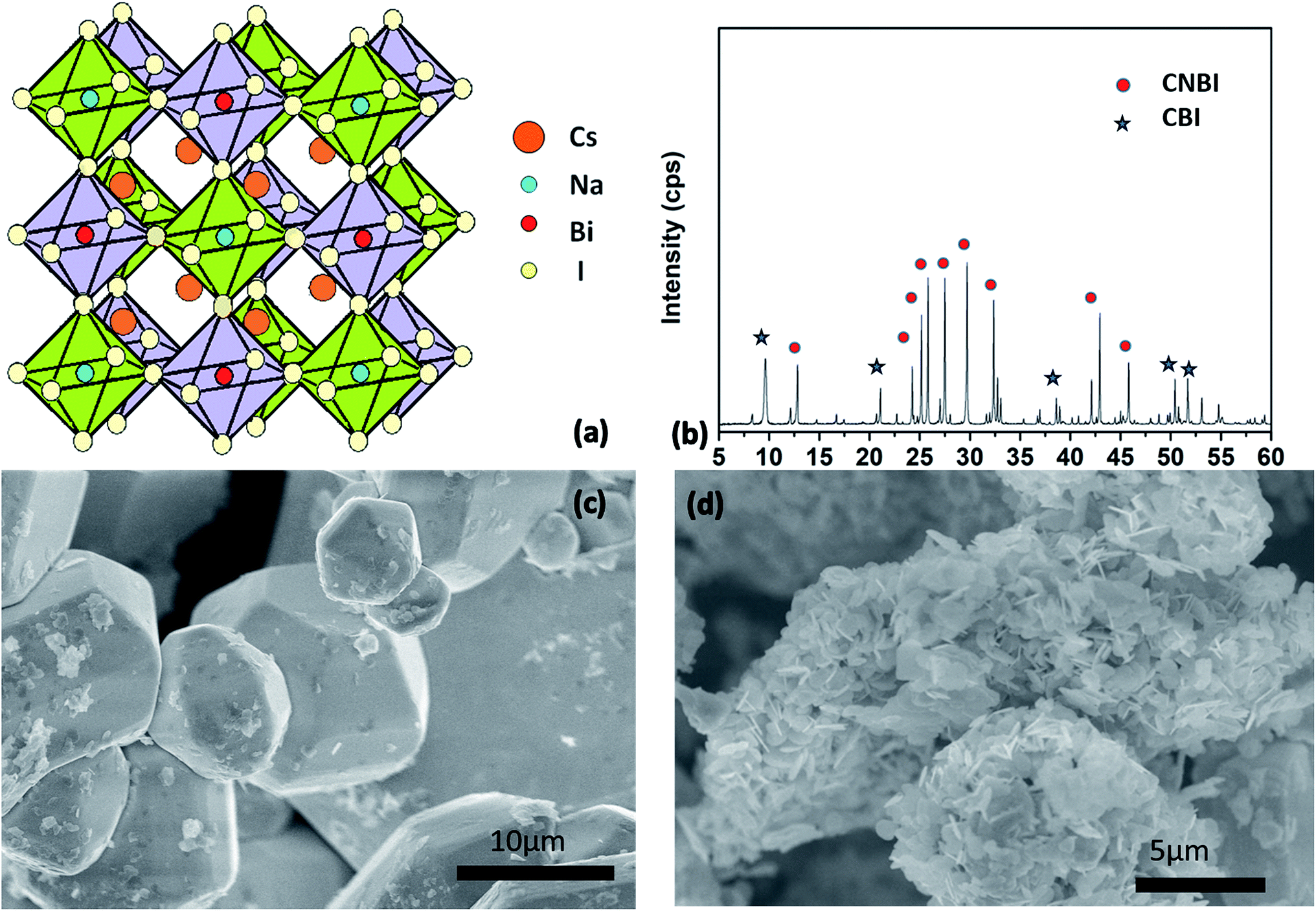 | ||
| Fig. 1 (a) Crystal structure of CNBI; (b) XRD pattern of the as-prepared CNBI powder. Red dots denote characteristic peaks of CNBI (Cs2NaBiI6) compared to the ref. 21 and blue stars denote some characteristic peaks belonging to the secondary phase, Cs3Bi2I9; SEM images showing (c) multiple shuttle-like crystals from high acidity synthesis and (d) clusters of nano-plates from non-acid synthesis. | ||
Cs3Bi2I9 (CBI) (Fig. 1(b)) is a secondary phase formed by the decomposition of CNBI. CBI has lower intensity than CNBI at 9.6, 21.1, 38.5, 50.4 and 51.5° (labelled as stars). Cs3Bi2I9 has been reported as a two-dimensional crystal structure with two face-sharing metal-halide octahedrons separated by cesium ions.11 During the chemical processes, when the temperature drops, some double perovskite CNBI species undergo partial decomposition while forming CBI.
| 2Cs2NaBiI6 ↔ CsI + 2NaI + Cs3Bi2I9 |
For further clarification, the overall chemical process is described below:
Initially, the formation of CBI is favourable due to over-saturation of the reaction solution (CsI and BiI3), in accordance with the Le Chatelier's principle.
| 3CsI + 2BiI3 → Cs3Bi2I9 |
As the temperature increases, CBI is completely dissolved in the reaction solution. Gradually, the reaction solution reverts to the over-saturation condition with the decrease in the solution's temperature; thus, CNBI is precipitated.
| 2CsI + 2NaI + BiI3 → Cs2NaBiI6 |
After a certain temperature threshold, CNBI partially decomposes, and the decomposition process continues until it reaches an equilibrium state. Assuming that CNBI is fully decomposed, the produced CsI and NaI can be eliminated completely during the post treatment process. Hence, it is hypothesized that the partial decomposition process occurs (forming CBI), and the decomposition process ceases upon reaching the equilibrium state.
| 2Cs2NaBiI6 ↔ CsI + 2NaI + Cs3Bi2I9 |
Based on the above-mentioned equation, according to the Le Chatelier's principle, we can deduce that the equilibrium reaction is more likely to favour the formation of CNBI with higher iodide anion concentration. Additionally, the temperature of the synthesis process also plays a crucial role, but it is not the key factor because the decomposition temperature is lower than the synthesis temperature.
Fig. 1(c) and (d) show scanning electron microscopy (SEM) images of the target product synthesized with and without the presence of an acid. The typical 3D structure of CNBI particles with smooth surfaces was formed in acidic conditions. The size of the 3D crystal was approximately several micrometres with a thickness of ∼20 μm. Unlike the results obtained for acidic conditions, plate particles of smaller and irregular shapes (composed of numerous 2D flake-like crystals) were formed when CNBI was grown in non-acidic conditions.
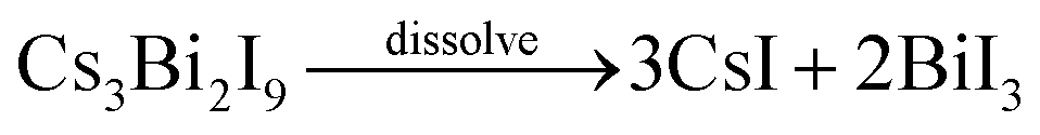
Fig. 2 displays the XPS spectra of CNBI. The full range survey of CNBI (Fig. 2(a)) explicitly revealed the presence of all CNBI elements (Na, Bi, Cs, and I) with binding energies in the range of ∼1000 eV to 150 eV. The binding energy of the spectra was adjusted with the carbon reference, which showed the 1s orbital peak at 282.2 eV, giving the charge correction factor Δ = 2.6 eV. Fig. 2(b) shows the narrow scan of Na 1s spectrum. The Na 1s orbital exhibited a significant peak at 1070 eV, which indicated the existence of both ionic sodium and sodium oxide. A NaKL1 Auger peak located at 497 eV, however, suggested the presence of only ionic sodium without the existence of sodium oxides, since it is known that for ionic sodium, 1s orbital and Auger peak always simultaneously appear in the XPS spectra.25 Herein, the two deconvoluted Na 1s peaks confirmed the formation of Na1+ ions in the as-prepared sample. The narrow scan of the Bi 4f spectrum (Fig. 2(c)) exhibited two deconvoluted peaks, which were Bi 4f5/2 and Bi 4f7/2 peaks, and they appeared at 158 eV and 164 eV, respectively. The binding energy difference of ∼5.3 eV proved the presence of Bi element with the oxidation state of 3+.26 Additionally, Cs 3d (Fig. 2(d)) indicated binding energies of 723 eV (Cs 3d3/2) and 736 eV (Cs 3d5/2), whereas I 3d (Fig. 2(e)) showed two strong deconvoluted peaks at binding energies of 617 eV and 629 eV, representing I 3d3/2 and I 3d5/2, respectively. Each spectrum showed well-separated spin–orbit peak components with standard binding energy differences. These peaks implied the formation of Cs, Bi and I ions with dominant valences of 1+, 3+ and 1−, respectively, thereby proving the formation of CNBI perovskite material.
 | ||
| Fig. 2 XPS spectra: (a) the full range survey and (b–e) narrow scans of CNBI; to be specific, the narrow scan spectra refer to (b) Na 1s, (c) Bi 4f, (d) Cs 3d, and (e) I 3d. | ||
By calculating the integrated peak areas of the XPS spectra, we can roughly estimate the molar ratio of the elements using the equation below:

![[thin space (1/6-em)]](https://www.rsc.org/images/entities/char_2009.gif) :Bi possessed a molar ratio of 1:4.9. Corroborating the decomposition process mentioned above, we can assume that about 2/3 of CNBI decomposed into CBI during the cooling process. This also indicated that our chemical hypothesis is viable.
:Bi possessed a molar ratio of 1:4.9. Corroborating the decomposition process mentioned above, we can assume that about 2/3 of CNBI decomposed into CBI during the cooling process. This also indicated that our chemical hypothesis is viable.
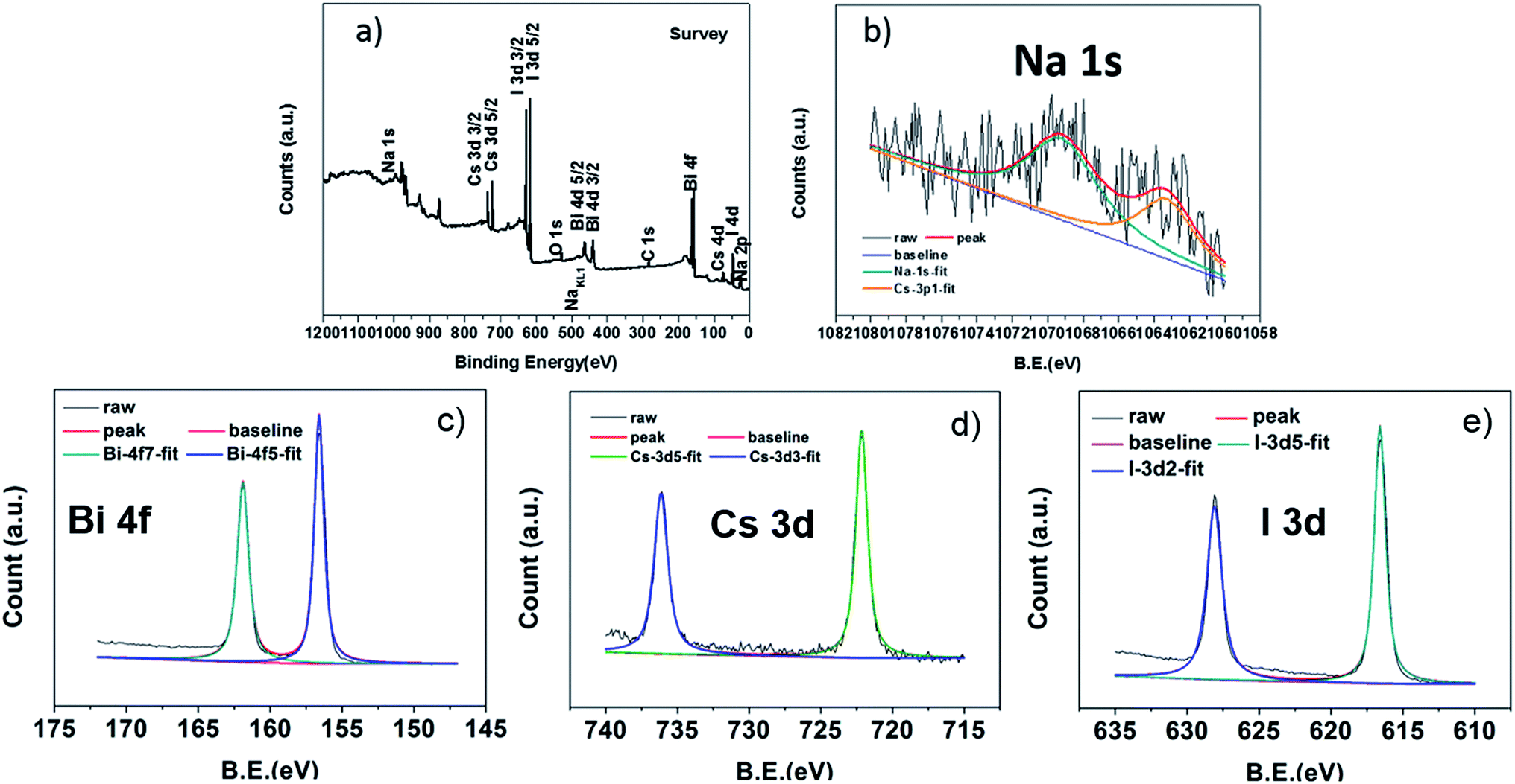
We have also revealed that hydroiodic acid plays an important role in controlling the crystal growth preference during the crystal assembling process. XRD test was performed to determine the crystal structure of CNBI synthesized using different acid concentrations such as 1, 3, 6 and 9 mol L−1, as shown in Fig. 3(a). Overall, the XRD data of all the synthesized CNBI samples matched perfectly and were reproducible regardless of the acid concentrations employed; this showed that the intensities of the CBI peaks gradually decreased in conjunction with the increase in the acid concentration, showing that decomposition was less significant, whereas the formation of CNBI was more dominant. We can say that the increasing acid concentration suppressed decomposition and promoted the formation of our target CNBI compound. We conclude that the amount of hydroiodic acid (HI) used in the synthesis process is the main factor favouring the formation of the CNBI phase.
 | ||
| Fig. 3 (a) XRD patterns, (b) optical absorption and (c, d, e, and f) SEM images of CNBI-1M, CNBI-3M, CNBI-6M and CNBI-9M, respectively, synthesized using different hydroiodic acid concentrations. The characteristic peaks of the secondary phase CBI located at 50.5 degree are significantly reduced with respect to the intensity when the concentration of acid increases. The absorption edges also decreased as observed from optical absorption analysis. | ||
To investigate the viability of CNBI as a light absorber, UV-vis absorption spectroscopy of the powder sample was performed to evaluate its light absorption ability and optical properties. Fig. 3(b) shows the optical absorption measurements of the synthesized CNBI samples at different HI concentrations. The results reveal that the CNBI sample obtained using 6 M HI during the synthesis possesses the best light absorbing ability; this could be due to the fact that the usage of 6 M HI optimizes and induces conducive conditions for the growth of a highly crystalline CNBI crystal structure. The CNBI powder exhibited excellent light absorption ranging from 300 nm to 600 nm with an absorption edge at 650 nm. The wide light-absorption range of the CNBI material is an important property and a core criterion for photovoltaic applications. Comparatively, it was clear that CNBI double perovskite possessed stronger absorption below 350 nm than a lead-based perovskite material, as the lead-based perovskite material usually shows decreased absorption.27 This suggested that CNBI can harvest extra energy in the ultraviolet region to enhance photocurrent conversion. In addition, the Tauc plot of the CNBI photoactive material is depicted as an inset image (Fig. 3(b)). By extrapolation, the band gap of the CNBI material was estimated to be 1.66 eV, which is suitable for application in photovoltaic devices in accordance with the Shockley–Queisser limit theory.28
A highly crystallized CNBI material synthesized at high acid concentrations was observed from the SEM images (Fig. 3), indicating that a highly acidic reaction process favours and promotes the crystallization of the double perovskite material, which was in agreement with the optical absorption spectra (Fig. 3(b)). The morphology of CNBI synthesized at 1 M acid concentration (Fig. 3(c)) presented an irregular bulk shape. Clearly, the 2D plates were randomly organized and stuck to the surfaces of the bulk CNBI, subsequently roughening the CNBI surfaces. In contrast, CNBI grew larger with smoother and cleaner surfaces (Fig. 3(d)) with the increase in acid concentrations such as with 3 mol L−1. Multiple shuttle-like CNBI crystals (Fig. 3(e)) were formed when the colloidal solution reached super-saturation at an acid concentration of 6 M. To further elaborate, at higher acidic or temperature conditions, the equilibrium of the perovskite colloidal solution was disturbed; consequently, the colloids were attacked and dissolved, which was followed by the release of reagent ions and continual formation of a super-saturated mixture and thus, CNBI continually crystallized until a new equilibrium state was attained.29 The larger CNBI particles prepared at 6 M HI concentration compared to those at 3 M were probably formed due to the differences in the crystal structures, as observed in the XRD patterns, and they showed different crystallization preferences. However, a further increase in the HI concentration did not improve the crystal growth. In contrast, agglomeration of the shuttle-like particles was observed on the surface of CNBI at a high HI concentration of 9 M.
Fig. 4 displays the SEM images of CNBI with a morphological structure of hexagonal plate at the 6 M acid concentration condition. This observation is in agreement with our prediction regarding the XRD patterns. The crystal growth mechanism (Fig. 4(a)) of CNBI is elucidated by inspecting the SEM images (Fig. 4 (b)–(e)) at different crystal growth times. It is observable that CNBI is a bulky crystal having a size of several tens of micrometres. The fully grown large crystals are obtained due to both the acidic solution environment and the high pressure-enclosed hydrothermal process.
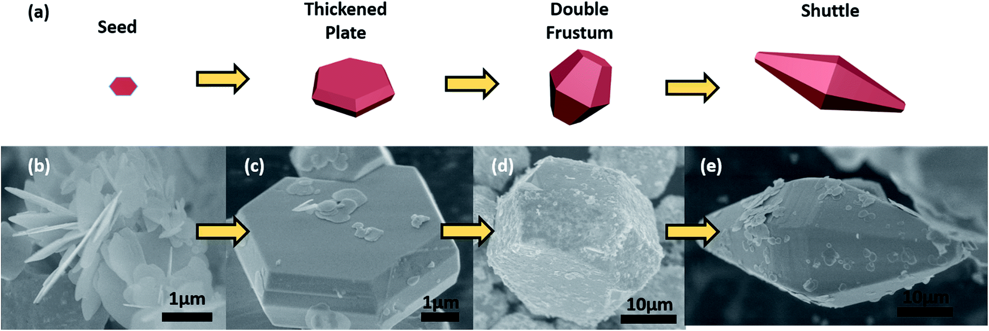 | ||
| Fig. 4 Scheme of the crystal growth mechanism and corresponding SEM images of as-prepared CNBI. Here, (a) shows sequential growth steps of the CNBI crystal, whereas (b)–(e) are the corresponding SEM images of the crystals at different growth steps. | ||
In our case, it is clear that the increase in temperature during the hydrothermal process does not merely disturb the acid–base equilibrium; in addition, the rising temperature causes more colloids to dissolve, and this disturbance generates a super-saturation condition. When the super-saturation condition is first reached, CNBI crystal seeds are formed, and they start to grow along the (001) plane, forming hexagonal platelets, as shown in Fig. 4(a). As the synthesis process continues, the CNBI-containing solution gradually becomes “depleted”, which results in an imbalance in the equilibrium; this causes more colloids to dissolve and further promotes the crystallization process. At this stage, the plate not only grows along the plane but also thickens on both sides, generating a thickened plate (Fig. 4(c)). It is shown that the size of the plate increases dramatically. However, with a longer synthesis time, the crystal growth along the (001) plane is hindered, and the crystal starts to preferentially grow in both directions perpendicular to the (001) plane, thus forming a double frustum, as shown in Fig. 4(d). The large CNBI crystal continues to grow during this continual super-saturation, subsequently initiating the crystallization process and eventually forming a fully grown crystal with shuttle-like morphology, as shown in Fig. 4(e). It is also noticeable that the shuttle-like crystal does not necessarily grow symmetrically with its centre plane, as shown in Fig. S2(a) and (b).† We also think that the asymmetric growth can be due to insufficient space.
Obtaining a perovskite material that is highly stable and resistant to harsh outdoor conditions is of primary importance for practical photovoltaic application and commercialization. Prior to solar cell fabrication, we also investigated the stability performance of our synthesized CNBI double perovskite material under ambient conditions. Specifically, we stored the sample in a colourless transparent vessel in ambient air for 5 months. From the XRD profile in Fig. 5(a), we observed that the XRD patterns of both fresh and stored (after 5 months) CNBI double perovskite samples were very similar, showing no occurrence of new peaks and no sign of further degradation. Please note that secondary phase CBI did not hinder the stability of the sample, due to CBI itself also being a relatively stable material. The intensity of CNBI's characteristic peaks did not significantly decrease, implying that the sample maintained good crystallinity. In addition, the width of CNBI characteristic peaks did not increase, suggesting that the particle size of the as-prepared sample did not undergo significant change. Overall, we can conclude that the as-prepared sample possesses excellent stability in ambient air (negligible degradation after 5 months of storage) and is highly resistant to moisture despite being stored at a high humidity of 70% from March to August. In brief, the remarkably stable CNBI double perovskite material has the potential to overcome the stability issues of the current perovskite solar cells. Fig. 5(b) shows dark red CNBI powder freshly synthesized according to the method described in the Experimental section. The powder can be dissolved in DMF at a concentration of 1.0 mg mL−1 and filtered to form a transparent dark red solution, also shown in Fig. 5(b). The solutions of both fresh and stored samples were spin-cast onto m-TiO2/c-TiO2/FTO glass to form uniform films (Fig. 5(c) and (d), respectively) with good crystallinity. The films showed similar colour. This also indicated that the sample retained good stability in ambient air. In addition, the fresh CNBI device was stored in ambient air for 14 days. The performances of the cells are presented in the ESI.† PCEs of the cells showed slight decrease after storage. VOC remained almost the same, showing that there were no extra recombination centres generated. This also agreed with our conclusion that the material is stable in ambient air. The decrease in the JSC value was observed due to the damage to the HTM layer and the gold electrode. These performances showed that the CNBI solar cells have good stability against ambient conditions.
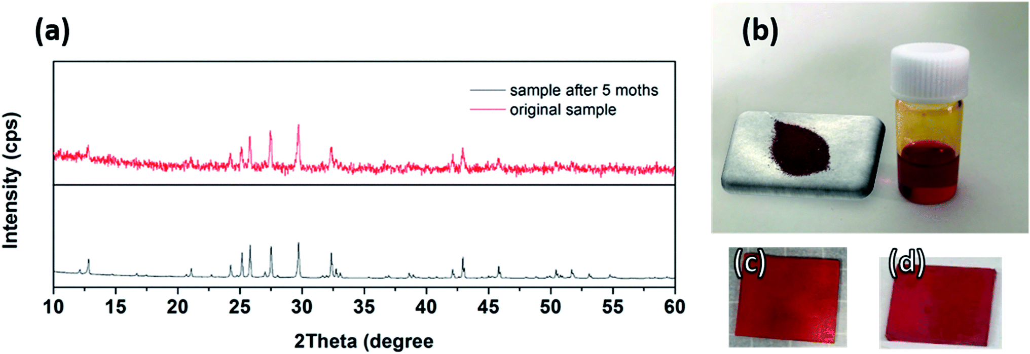 | ||
| Fig. 5 (a) XRD pattern comparison of fresh CNBI and the same sample after 5 months storage. (b) Fresh sample and its solution in DMF. (c) A film fabricated with fresh sample and (d) with the sample stored for 5 months. | ||
Double perovskite solar cells composed of TiO2 as the ETL and spiro-OMeTAD as the HTM were fabricated under ambient conditions, without the usage of a glovebox, as shown in Fig. 6. Fig. 6(c) shows the J–V curve of CNBI double perovskite solar cell, which exhibited the highest PCE. The CNBI double perovskite-based solar cell exhibited PCE of 0.42%, VOC of 0.47 V, FF of 0.44, and JSC of 1.99 mA cm−2, which were comparable to the results of other lead-free perovskite solar cells reported in the literature (Table 1). The testing of multiple devices yielded VOC of 0.45 ± 0.02 V, FF of 0.40 ± 0.04, and JSC of 1.80 ± 0.20 mA cm−2. The histogram of the PCE distribution for a batch of 30 solar cells is presented in Fig. 6(d), and the PCEs obtained ranged from 0.27–0.42%. Overall, the CNBI double perovskite material has high potential to replace unstable and toxic organic lead-based perovskite materials once satisfactory PCE performance of the double perovskite has been achieved. One disadvantage of the CNBI solar cell is low JSC, which indicates significant recombination generated from trapping centres or even pinholes caused by large grain size. We also measured the EQE curve of the CNBI solar cell, as shown in Fig. 6(e). We observed that the device showed a quantum efficiency of about 20% from 300 to 500 nm. Compared to the UV-vis absorption spectrum, EQE at 500–600 nm was low; this suggested that in this range, CNBI cannot effectively convert excitons to current, and a portion of the incident solar energy is lost. This is one of the important reasons for the cells' low JSC. It is notable that the film's qualities, such as the presence of traps and inhomogeneity, also contribute to low EQE and JSC. Thus, improving the film quality is important to enhance the EQE performance.
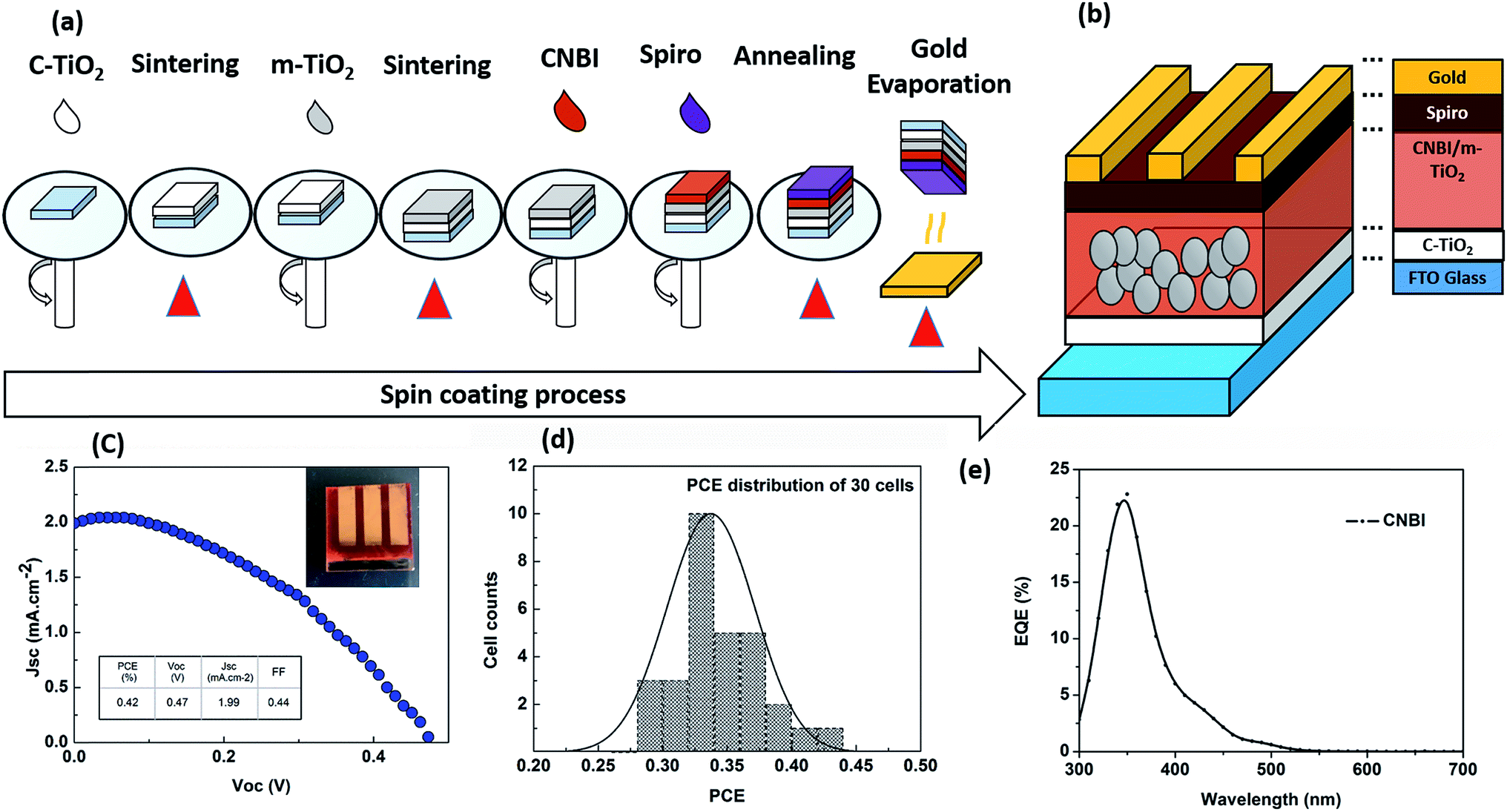 | ||
| Fig. 6 Structure and performance of CNBI solar cell. (a) Cell fabrication process, (b) device configuration diagram, (c) J–V curve of the best performing cell and (d) power conversion efficiency distribution. (e) The comparison of the EQE curve and the UV-vis absorption curve of the CNBI solar cell. | ||
To confirm the viability of the device structure, we have tested the band positions of CNBI and the related ETM/HTM material. By testing the HOMO position and calculating the obtained band gap, the band positions of CNBI were obtained, as shown in Fig. 7(a) and (b). We observed that the LUMO of CNBI was quite near to that of ETM, which hindered electron injection. Also, the HOMO of CNBI was nearer to that of HTM compared to the observations for lead perovskites, which hindered hole collection. We have discussed that our material has relatively low hole transport ability; thus, the weakened hole collecting ability is significant. These two factors are the major reasons for low JSC. Since our computational results showed that the hole transport ability of CNBI is low, a strong hole extraction layer is needed to improve the performance. In our case, spiro-OMeTAD is clearly not a superior choice. Further optimization will include the improvement of the film quality and the selection of a superior hole transport material.
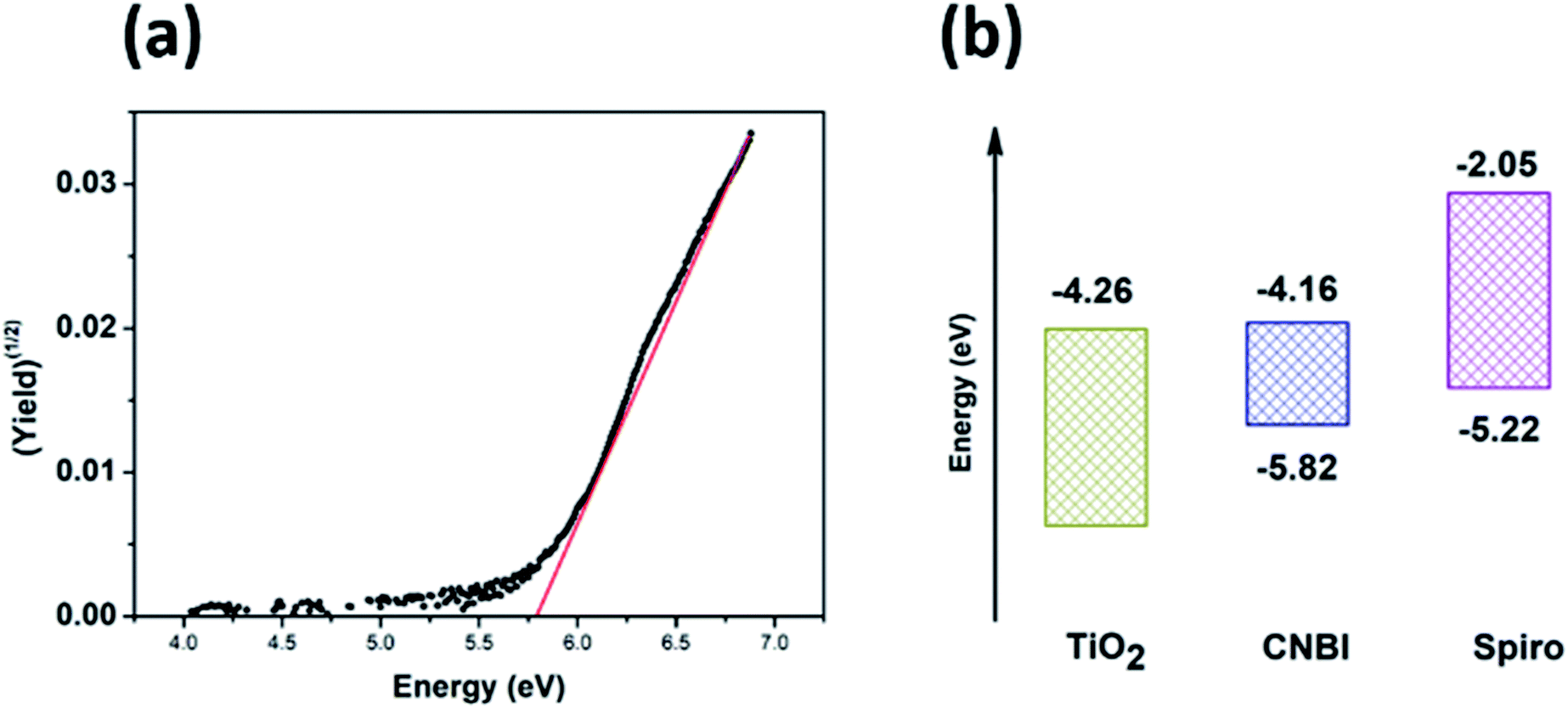 | ||
| Fig. 7 (a) HOMO position test curve and (b) band positions of CNBI, ETM (TiO2) and HTM (spiro-OMeTAD). | ||
4. Conclusions
In conclusion, we have successfully synthesized a novel, cost-effective, and highly stable double perovskite CNBI photo-active material via a facile hydrothermal process. The unique shuttle-like 3D CNBI material has a band gap of 1.66 eV. In addition, CNBI double perovskite's wide absorption range and remarkable stability (negligible degradation after 5 months of storage at relative humidity of 70%) match the criteria for photovoltaic application. Preliminary tests have been performed for CNBI double perovskite solar cell where the best CNBI solar cell exhibited PCE of 0.42%, which is comparable to those of other lead-free perovskite solar cells. The narrow distribution of PCEs suggests that the material has good stability and reproducibility with respect to device fabrication. Although the obtained PCE of CNBI so far is considered low, by further optimization inputs, CNBI can be a promising non-toxic and stable substituent over hazardous lead halide perovskite materials. Our future research efforts will focus on fabricating high-quality CNBI films to fulfil the requirements for a photovoltaic device. Apart from the applications in solar cells, CNBI can also be used for other interesting applications such as in LEDs and lasers.Conflicts of interest
There are no conflicts to declare.Acknowledgements
This work was supported by the Grant-in-Aid for Scientific Research (KAKENHI) program, Japan (C, Grant Number 15K05597) and Takahashi Industrial and Economic Research Foundation (Takahashi Grant Number 06-003-154).References
- T. Koh, K. Fu, Y. Fang, S. Chen, T. Sum and N. Mathews, et al., Formamidinium-Containing Metal-Halide: An Alternative Material for Near-IR Absorption Perovskite Solar Cells, J. Phys. Chem. C, 2014, 118, 16458–16462 Search PubMed.
- M. Lee, J. Teuscher, T. Miyasaka, T. Murakami and H. Snaith, Efficient Hybrid Solar Cells Based on Meso-Superstructured Organometal Halide Perovskites, Science, 2012, 338(6107), 643–647 CrossRef PubMed.
- Q. Dong, Y. Fang, Y. Shao, P. Mulligan, J. Qiu and L. Cao, et al., Electron-hole diffusion lengths > 175 μm in solution-grown CH3NH3PbI3 single crystals, Science, 2105, 347(6225), 967–970 CrossRef PubMed.
- B. Yang, O. Dyck, J. Poplawsky, J. Keum, A. Puretzky and S. Das, et al., Perovskite Solar Cells with Near 100% Internal Quantum Efficiency Based on Large Single Crystalline Grains and Vertical Bulk Heterojunctions, J. Am. Chem. Soc., 2015, 137(29), 9210–9213 CrossRef PubMed.
- R. Brandt, V. Stevanovic, D. Ginlev and T. Buonassisi, Identifying defect-tolerant semiconductors with high minority carrier lifetimes: Beyond hybrid lead halide perovskites, MRS Commun., 2015, 5, 265–275 CrossRef.
- T. Berhe, W. Su, C. Chen, C. Pan, J. Cheng and H. Chen, et al., Organometal halide perovskite solar cells: degradation and stability, Energy Environ. Sci., 2015 Oct 20, 9, 323–356 Search PubMed.
- J. Feng and B. Xiao, Effective Masses and Electronic and Optical Properties of Nontoxic MASnX3 (X = Cl, Br, and I) Perovskite Structures as Solar Cell Absorber: A Theoretical Study Using HSE06, J. Phys. Chem. C, 2014, 118(34), 19655–19660 Search PubMed.
- N. Noel, S. Stranks, A. Abate, C. Wehrenfennig, S. Guarnera and A. Haghighirad, et al., Lead-free organic–inorganic tin halide perovskites for photovoltaic applications, Energy Environ. Sci., 2014, 7, 3061–3068 Search PubMed.
- B. Park, B. Philippe, X. Zhang, H. Rensmo, G. Boschloo and E. Johansson, Bismuth Based Hybrid Perovskites A3Bi2I9 (A: Methylammonium or Cesium) for Solar Cell Application, Adv. Mater., 2015 Sep 29, 27(43), 6806–6813 Search PubMed.
- T. Krishnamoorthy, H. Ding, C. Yan, W. Leong, T. Baikie and Z. Zhang, et al., Lead-free germanium iodide perovskite materials for photovoltaic applications, J. Mater. Chem. A, 2015, 3, 23829–23832 Search PubMed.
- X. Cui, K. Jiang, J. Huang, Q. Zhang, M. Su and L. Yang, et al., Cupric bromide hybrid perovskite heterojunction solar cells, Synth. Met., 2015, 209, 247–250 CrossRef.
- M. Pazoki, T. Jacobsson, A. Hagfeldt, G. Boschloo and T. Edvinsson, Effect of metal cation replacement on the electronic structure of metalorganic halide perovskites: Replacement of lead with alkaline-earth metals, Phys. Rev. B, 2016, 93, 144105 CrossRef.
- H. Zhou, Q. Chen, G. Li, S. Luo, T. Song and H. Duan, et al., Interface engineering of highly efficient perovskite solar cells, Science, 2014, 345(6196), 542–546 CrossRef PubMed.
- C. Wu, Q. Zhang, Y. Liu, W. Luo, X. Guo and Z. Huang, et al., The Dawn of Lead-Free Perovskite Solar Cell: Highly Stable Double Perovskite Cs2AgBiBr6 Film, Adv. Sci., 2017, 5(3), 1700759 CrossRef PubMed.
- Z. Xiao, M. Meng, J. Wang and Y. Yan, Thermodynamic Stability and Defect Chemistry of Bismuth-Based Lead-Free Double Perovskites, ChemSusChem, 2016, 9(18), 2628–2633 CrossRef PubMed.
- G. Volonakis, M. Filip, A. Haghighirad, N. Sakai, B. Wenger and H. Snaith, et al., Lead-Free Halide Double Perovskites via Heterovalent Substitution of Noble Metals, J. Phys. Chem. Lett., 2016, 7(7), 1254–1259 CrossRef PubMed.
- F. Wei, Z. Deng, S. Sun, F. Zhang, D. Evans and G. Kieslich, et al., Synthesis and Properties of a Lead-Free Hybrid Double Perovskite: (CH3NH3)2AgBiBr6, Chem. Mater., 2017, 29(3), 1089–1094 CrossRef.
- M. Filip, S. Hillman, A. Haghighirad, H. Snaith and F. Giustino, Band Gaps of the Lead-Free Halide Double Perovskites Cs2BiAgCl6 and Cs2BiAgBr6 from Theory and Experiment, J. Phys. Chem. Lett., 2016, 7(13), 2579–2585 CrossRef PubMed.
- A. Slavney, T. Hu, A. Lindenberg and H. Karunadasa, A Bismuth-Halide Double Perovskite with Long Carrier Recombination Lifetime for Photovoltaic Applications, J. Am. Chem. Soc., 2016, 138(7), 2138–2141 CrossRef PubMed.
- E. McClure, M. Ball, W. Windl and P. Woodward, et al., Cs2AgBiX6 (X = Br, Cl): New Visible Light Absorbing, Lead-Free Halide Perovskite Semiconductors, Chem. Mater., 2016, 28(5), 1348–1354 CrossRef.
- P. Cheng, T. Wu, Y. Li, L. Jiang, W. Deng and K. Han, et al., Combining theory and experiment in the design of a lead-free ((CH3NH3)2AgBiI6) double perovskite, New J. Chem., 2017, 41, 9598–9601 RSC.
- G. Volonakis, A. Haghighirad, R. Milot, W. Sio, M. Filip and B. Wenger, et al., Cs2InAgCl6: A New Lead-Free Halide Double Perovskite with Direct Band Gap, J. Phys. Chem. Lett., 2017, 8(4), 772–778 CrossRef PubMed.
- F. Wei, Z. Deng, S. Sun, F. Xie, G. Kieslich and D. Evans, et al., The synthesis, structure and electronic properties of a lead-free hybrid inorganic–organic double perovskite (MA)2KBiCl6 (MA = methylammonium), Mater. Horiz., 2016, 3, 328–332 RSC.
- R. Shannon, Revised effective ionic radii and systematic studies of interatomic distances in halides and chalcogenides, Acta Crystallogr., 1976, A32, 751–767 CrossRef.
- M. Lyu, J. Yun, M. Cai, Y. Jiao, P. Bernhardt and M. Zhang, et al.,, Nano Res., 2016, 9(3), 692–702 CrossRef.
- C. Ng, H. Lim, S. Hayase, Z. Zainal, S. Shafie and N. Huang, Effects of Temperature on Electrochemical Properties of Bismuth Oxide/Manganese Oxide Pseudocapacitor, Ind. Eng. Chem. Res., 2018, 57(6), 2146–2154 CrossRef.
- A. Leguy, P. Azarhoosh, M. Alonso, M. Campoy-Quiles, O. Weber and J. Yao, et al., Experimental and theoretical optical properties of methylammonium lead halide perovskites, Nanoscale, 2016, 8, 6317–6327 RSC.
- M. Shockley and H. Queisser, Detailed Balance Limit of Efficiency of p–n Junction Solar Cells, J. Appl. Phys., 1961, 32, 510–519 CrossRef.
- P. Nayak, D. Moore, B. Wenger, S. Nayak, A. Haghighirad and A. Fineberg, et al., Mechanism for rapid growth of organic–inorganic halide perovskite crystals, Nat. Commun., 2016, 7, 13303 CrossRef PubMed.
- M. Johansson, H. Zhu and E. Johansson, Extended Photo-Conversion Spectrum in Low-Toxic Bismuth Halide Perovskite Solar Cells, J. Phys. Chem. Lett., 2016 Aug 19, 7(17), 3467–3471 Search PubMed.
- C. Ran, Z. Wu, J. Xi, F. Yuan, H. Dong and T. Lei, et al., Construction of Compact Methylammonium Bismuth Iodide Film Promoting Lead-Free Inverted Planar Heterojunction Organohalide Solar Cells with Open-Circuit Voltage over 0.8 V, J. Phys. Chem. Lett., 2017, 8(2), 394–400 CrossRef PubMed.
- J. Hebig, I. Kühn, J. Flohre and T. Kirchartz, Optoelectronic Properties of (CH3NH3)3Sb2I9 Thin Films for Photovoltaic Applications, ACS Energy Lett., 2016, 1(1), 309–314 CrossRef.
- T. Singh, A. Kulkarni, M. Ikegami and T. Miyasaka, Effect of Electron Transporting Layer on Bismuth-Based Lead-Free Perovskite (CH3NH3)3Bi2I9 for Photovoltaic Applications, ACS Appl. Mater. Interfaces, 2016, 8(23), 14542–14547 Search PubMed.
- B. Ghosh, B. Wu, H. Mulmudi, C. Guet, K. Weber and T. Sum, et al. , ACS Appl. Mater. Interfaces, 2018 DOI:10.1021/acsami.7b14735.
Footnote |
| † Electronic supplementary information (ESI) available. See DOI: 10.1039/c8se00154e |
| This journal is © The Royal Society of Chemistry 2018 |