
Quantitative analysis of the transient photoluminescence of CH3NH3PbI3/PC61BM heterojunctions by numerical simulations†
Benedikt
Krogmeier
 a,
Florian
Staub
a,
David
Grabowski
a,
Uwe
Rau
a and
Thomas
Kirchartz
*ab
a,
Florian
Staub
a,
David
Grabowski
a,
Uwe
Rau
a and
Thomas
Kirchartz
*ab
aIEK5-Photovoltaik, Forschungszentrum Jülich, 52425 Jülich, Germany. E-mail: t.kirchartz@fz-juelich.de
bFaculty of Engineering and CENIDE, University of Duisburg-Essen, Carl-Benz-Str. 199, 47057 Duisburg, Germany
First published on 2nd March 2018
Abstract
Transient photoluminescence measurements of lead-halide perovskite layers with electron or hole transport layers provide insights into the interfacial charge transfer and recombination processes. However, analytically describing these measurements over a wide range of timescales is complicated by the combination of different physical effects such as transport within the perovskite, transfer to the transport layer, accumulation of charges and recombination at the interface. Therefore, numerical drift-diffusion simulations of photoluminescence transients as a function of laser fluence and interface properties are used to obtain a quantitative understanding of experimental results. Comparison between experiment and simulation combined with an analysis of the uniqueness of the result yields an interface-recombination velocity that has to be around ∼200 cm s−1 for the perovskite–PC61BM interface in order to be consistent with data obtained at several laser fluences.
1. Introduction
The insights obtained from transient photoluminescence (PL) measurements have contributed to an improved understanding of recombination and transport in a wide range of semiconductors including many materials used for optoelectronic or photovoltaic applications such as III-Vs,1–3 Cu(In,Ga)Se2,4–11 CdTe,12–14 kesterite15,16 and recently also metal-halide perovskites.17–24 Transient photoluminescence is attractive because it allows contactless measurements of films on glass, layer stacks or complete devices while studying processes on different time- and length-scales. In particular, it permits analysis of the various recombination processes that happen in photovoltaic absorber materials and that may reduce the open-circuit voltage and subsequently the efficiency of solar cells made from these materials.25For doped semiconductor films, analyzing data is often fairly straightforward due to the PL decay being dominated by minority-carrier recombination via a particular loss channel such as bulk defects or surface defects.1 Analyzing luminescence transients measured on samples with low doping concentrations (such as lead-halide perovskites20,26), however, is more challenging because the transients could be affected not only by recombination but also by charge transfer of either of the two charge carriers into an adjacent layer. Studying the charge-carrier dynamics at the interfaces between lead-halide perovskites and electron or hole contact layers is of particular interest because these dynamics might help clarifying crucial properties related to charge extraction and charge recombination27–34 at these interfaces. In the case of measurements performed on lead-halide perovskite layers in contact with any electron or hole transport layers, the transients have been interpreted either as a signature of the electron or hole mobility in the perovskite17,35–37 or as the charge transfer to the contact layers38–48 and the interfacial recombination.49–53 In each of these cases, assumptions have to be made that one of several processes is the fastest process and therefore dominating the rate. This approach allows an analytical description of the shape of the decay transient. However, it is currently not clear which information we could extract from photoluminescence transients of intrinsic solar cell absorber materials in contact with electron or hole accepting transport layers in general and of metal-halide perovskite layers in particular.
The present paper provides a complete numerical description of transport, transfer and recombination processes happening at the interface between metal-halide perovskite films and electron or hole transport layers. Numerical simulations are an established method to model and understand processes in thin-film solar cells.11,14,54–60 Transient drift-diffusion simulations taking into account electrostatic effects have been employed to simulate transient photoluminescence experiments in a range of material systems and devices used in photovoltaics.8–10,14,15,61 However, the specific case of transient drift-diffusion simulations of photoluminescence in metal-halide perovskites is currently not well explored. For metal-halide perovskites, the focus so far has either been on the solution of rate equations49,50 or the solution of the diffusion equation17 neglecting electrostatic effects.
We show using numerical simulations, which include electrostatic effects that at short delay times after the pulse, charge transport and charge-transfer processes dominate the shape of the decay transient. At longer delay times, charge carriers that might build up in the transfer material can either recombine at the interface or be re-injected into the perovskite layer and recombine there. Thus, we expect to see two potentially but not necessarily distinguishable regimes of the transient that we interpret differently. After presenting the main effects that can affect the transients, we compare the simulations to experimental data acquired from lead-halide perovskite/PCBM samples enabling us to obtain the interface-recombination velocity SR and the transfer velocity ST of our sample. We find that numerical simulations are crucial for the understanding and analysis of PL transients, because of charge accumulation as well as various recombination and transport processes occurring on the same timescale. Furthermore, the present approach allows one to quantitatively analyze the functionality of a single contact, i.e. of a combination of a contact material and a photovoltaic absorber material without the need of completing a solar cell device.
2. Theory of non-linear effects in transient photoluminescence
For this study we consider our sample to be a type-II heterojunction of a methylammonium lead halide perovskite and an electron transfer material (here: phenyl-C61-butyric acid methyl ester, PC61BM), often called quencher layer in PL measurements. In order to minimize the potential effects of ion movement on the results, we chose PC61BM as a model electron transport layer because it is nominally undoped. Thus, there is little reason to assume that strong electric fields are created within the perovskite layer that lead to a redistribution of ionic charge in the device which may affect the longer time components of the transients. Fig. 1a shows as an example the band diagram of this heterojunction while a laser pulse hits the sample, thereby generating charge carriers. Diffusion causes the photo-generated charge carriers to move to the perovskite/quencher interface, and once electrons reach the interface, they can transfer to the lower conduction band of the quencher layer (Fig. 1a). The transfer-current density JT,n for electrons is given by the equation62,63 | (1) |
 | ||
| Fig. 1 Band diagram and PL transients of simulated perovskite (bulk) and PCBM (quencher) layers. (a) Band diagram during the laser pulse; charge carriers are generated in the bulk and electrons transfer to the quencher. (b) Band diagram for longer delay times; charge carriers accumulate at the interface leading to increased interfacial recombination. (c) TRPL signal for two laser fluences EL, both showing two slopes, one can be assigned to transfer and the other to interfacial recombination. (d) Differential lifetime showing two constant, clearly distinguishable regions for low laser fluences and a less distinguishable case for higher light intensities, due to accumulation of charge carriers. Note that the interface-recombination velocity is SR = 10 cm s−1 here and the laser fluences EL are 1 nJ cm−2 for (c) and (d) (low EL case) and 100 nJ cm−2 for (a), (b), (c) and (d) (high EL case). | ||
Once electrons have been transferred to the quencher (Fig. 1b), they will be attracted by holes in the bulk through Coulomb interactions, forcing the electrons in the quencher layer and the holes in the bulk layer to accumulate at the interface. The spatially changing charge carrier density due to accumulation will cause non-linearities in the system. Accumulated charge at the interface will have an impact on the PL, because the accumulated electrons can slow down the transfer by repelling electrons in the bulk, and the high interfacial charge carrier densities lead to increased interfacial recombination Rint, as given by the equation
 | (2) |
Two simulated PL transients resulting from a perovskite/quencher sample are displayed in Fig. 1c. We express the photoluminescence photon flux ΦPL as
 | (3) |
PL transients of perovskite/quencher samples may show a continuously varying slope with time due to changing decay velocities with faster decays generally happening at earlier times (see Fig. 1c). The fast decay at short delay times for the cases shown in Fig. 1 is caused by the transfer of electrons to the quencher, and thereby a loss of bulk electrons np, while the second slope can be assigned to interfacial recombination, and thereby a loss of bulk holes pp. Charge-carrier densities in the quencher do not affect the PL due to the low luminescence efficiency of fullerenes69 and the relatively low hole density in PC61BM during the PL transient. We will show in this paper that due the non-linearities caused by charge carriers accumulating at the interface two slopes are not always clearly distinguishable, because the accumulating charges decrease the transfer current, but increase the interfacial recombination current. This effect can be seen at higher light intensities in Fig. 1c.
In literature, lifetimes have often been obtained by fitting a mono-exponential decay37,38,46 or bi-exponential decay36,44,45,51,52 function to the PL transient (ΦPL ∝ exp(−t/τPL)). The disadvantage of this method is that the model is chosen entirely based on the conceived shape of the transient. The model, especially one based on a bi-exponential decay, may not allow a clear assignment of the two lifetimes to the physical processes happening in the sample. In particular, this approach cannot take into account the impact of non-linearities caused by accumulated charge carriers. Instead of a mono- or bi-exponential decay, we define the differential lifetime τPL(t) as the inverse negative slope of the logarithmically plotted PL photon flux ΦPL, i.e.
 | (4) |
This approach of using a differential lifetime has the advantage that all information about how the decay changes with time is retained. This is a necessary prerequisite to study phenomena like charge accumulation that do not lead to a simple exponential or power-law behavior of the decay transient because they are non-linear. As an example Fig. 1d shows the differential lifetime calculated with eqn (4) of the PL decays displayed in Fig. 1c. For low laser fluences the two lifetimes resulting from transfer and from interfacial recombination are clearly distinguishable, while they are less easy to distinguish at higher light intensities due to stronger charge accumulation at the interface.
We model the perovskite/PC61BM heterojunction with the software TCAD Sentaurus by Synopsis. TCAD Sentaurus describes the processes happening during a PL transient by a set of differential equations. These equations are the continuity equations for electrons and for holes, for describing transport, generation and recombination processes and the Poisson equation, for describing the electrostatic interactions of charge carriers. Additionally, boundary conditions specify the processes occurring at interfaces and surfaces. Analytically solving these equations for spatially changing charge-carrier densities and with several processes happening on the same timescale is unfeasible. TCAD Sentaurus solves the equations numerically and enables us to analyze the impact that transfer, interfacial recombination and charge carrier accumulation have on the slopes of the PL decay of perovskite/PC61BM samples.
3. Impact of charge accumulation on differential lifetimes
To study the influence of interface defects on PL transients, we have changed the interface-recombination velocity SR by several orders of magnitude in the simulation. Fig. 2a displays the differential lifetime τPL calculated with eqn (4) from simulated PL transients (see Fig. S5a†) with a relatively low laser fluence of 1 nJ cm−2. The differential lifetime τPL features two clearly distinguishable time intervals where it remains constant: the first interval at short times is dominated by the transfer of electrons from the bulk into the quencher. The second interval at longer delay times is dominated by interfacial recombination of holes in the bulk with electrons in the quencher if surface recombination is high enough (SR = 10−1 cm s−1 to 103 cm s−1). For lower surface recombination velocities (e.g. SR = 10−2 cm s−1) and long delay times, the recombination in the bulk is higher than the interfacial recombination and electrons transfer back into the bulk, resulting in a differential lifetime that is lower than the interface-recombination lifetime would be. For the highest SR shown in Fig. 2a only transfer limits the lifetime; once the electrons reach the quencher, they recombine almost immediately. The transfer rate increases due to the low electron density nq,int at the interface in the quencher resulting from the high interface-recombination velocity.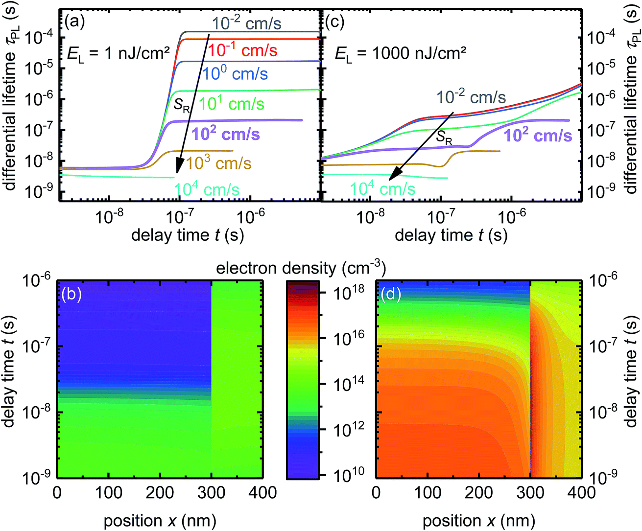 | ||
| Fig. 2 (a) Simulated differential lifetime at laser fluence EL = 1 nJ cm−2, showing two time regions where the differential lifetime is first dominated by transfer and eventually recombination. (b) Electron density for SR = 102 cm s−1 and 1 nJ cm−2 showing how electron density rises in the quencher due to transfer and decreases due to recombination. (c) The differential lifetime at a laser intensity of 1000 nJ cm−2 showing a more complicated situation than (a) due to transfer, recombination and accumulation occurring on the same timescale. (d) Electron density for SR = 102 cm s−1 and 1000 nJ cm−2 showing accumulation of electrons at the interface. See ESI Fig. S5a and S5b† for the PL transients. | ||
To have a better insight into what is happening to the charge-carrier density during the measurement, the electron density for the case SR = 102 cm s−1 and EL = 1 nJ cm−2 is plotted in Fig. 2b as a function of time and position. The electron density is almost equally distributed at the beginning directly after the laser pulse, but with advancing time, due to electron transfer the electron density decreases in the bulk and increases in the quencher until it reaches its peak value in the quencher. After the peak electron density in the quencher decreases due to interfacial recombination, the bulk electron density decreases slowly due to bulk recombination. The accumulation of electrons at the interface in the quencher layer is noticeable but not very strong; hence analytical solutions could still provide an accurate description for the case in Fig. 1a and b.
In the next case, we consider a much higher laser fluence of EL = 1000 nJ cm−2 and therefore a much higher photogenerated charge-carrier density. Fig. 2c shows the differential lifetime at a laser fluence of EL = 1000 nJ cm−2 for the same interface-recombination velocities as in Fig. 2a. The lifetime increases at short times and decreases at long times due to accumulation of charge carriers at the interface. The impact of charge accumulation is highest for low recombination velocities because interfacial recombination reduces the built-up of charges at the interface. Especially, for low recombination velocities and long delay times the change between Fig. 2a and c is enormous. This change shows that falsely interpreting the lifetime at long delay times as only caused by interfacial recombination and equally distributed charge carriers in the quencher could lead to strong deviations between the measured and the actual interface properties. Only for the cases at SR = 102 cm s−1 and 103 cm s−1, the differential lifetimes in Fig. 2c saturate at the same value as seen in Fig. 2a, indicating that interfacial recombination dominates the lifetime and transfer and accumulation are not relevant anymore. The differential lifetime at SR = 104 cm s−1 is again limited only by the transfer to the quencher.
Fig. 2d shows the electron density for one case (EL = 1000 nJ cm−2 and SR = 10 cm s−1). As expected, the electrons accumulate at the interface because of the Coulomb attraction. While the electron density in the bulk decreases due to electron transfer to the PC61BM, the electron density in the quencher stays almost the same for about 60 ns. This constant density indicates that the velocity of electrons transferring to the quencher and the velocity of electrons recombining at the interface are almost the same.
For longer times, the charge carrier density in the quencher decreases and the charges are distributed more equally in the quencher. Thus, the situation arises where the PL decay is no longer determined by transfer and accumulation but rather by interfacial recombination, which is the cause of the constant lifetime at long delay times (Fig. 2c, SR = 102 cm s−1). This constant lifetime coincides with the lifetime in Fig. 2a for the same interfacial recombination velocity (SR = 102 cm s−1).
Analyzing results to obtain the lifetime caused by interfacial recombination would be easiest and most precise at very low laser intensities, as charge carriers accumulation at the interface could be avoided. Unfortunately, the PL signal gained from such fluences would be too low to be accurately measured.
4. Extracting recombination velocities from experimental data
We use the insights obtained through simulations to explain the processes happening in a perovskite/PC61BM layer stack and to obtain parameters like the interface-recombination velocity and the transfer velocity. Fig. 3a displays the PL of a sample excited by three different light intensities. The shapes of the PL curves have a peculiar dependence on light intensity: measured at three laser fluences, the PL decays slow down going from 77 nJ cm−2 to 780 nJ cm−2 but accelerate going from 780 nJ cm−2 to 10![[thin space (1/6-em)]](https://www.rsc.org/images/entities/char_2009.gif) 000 nJ cm−2. We calculate the differential lifetime with eqn (4) from the measured data plotted in Fig. 3a, fit an arbitrary function to the differential lifetime and use the inverse of eqn (4) to get the fit shown in Fig. 3a. Fig. 3b shows the fit of the differential lifetime (for fit and data see Fig. S6†) which exhibits a similar dependence on the laser fluence intensity as seen for the PL in Fig. 3a. By comparing the value and the trend in Fig. 3a to the previously discussed lifetimes in Fig. 2b, the order of magnitude for transfer and interfacial recombination lifetime can be estimated, thereby enabling us to refine our parameters for the simulation. In previous work,20 we reported an external radiative-recombination coefficient krad = 4.78 × 10⁻¹¹ cm3 s−1 measured for single perovskite layers. Here, ‘external’ refers to the value of k before correction for photon recycling has taken place.70 However, from the simulations presented here, we estimated an increased value of krad = 1.4 × 10⁻¹⁰ cm3 s−1, based on the hypothesis that an additional PC61BM layer lowers the amount of photon recycling and therefore increases the external value of k for a given internal value of k.
000 nJ cm−2. We calculate the differential lifetime with eqn (4) from the measured data plotted in Fig. 3a, fit an arbitrary function to the differential lifetime and use the inverse of eqn (4) to get the fit shown in Fig. 3a. Fig. 3b shows the fit of the differential lifetime (for fit and data see Fig. S6†) which exhibits a similar dependence on the laser fluence intensity as seen for the PL in Fig. 3a. By comparing the value and the trend in Fig. 3a to the previously discussed lifetimes in Fig. 2b, the order of magnitude for transfer and interfacial recombination lifetime can be estimated, thereby enabling us to refine our parameters for the simulation. In previous work,20 we reported an external radiative-recombination coefficient krad = 4.78 × 10⁻¹¹ cm3 s−1 measured for single perovskite layers. Here, ‘external’ refers to the value of k before correction for photon recycling has taken place.70 However, from the simulations presented here, we estimated an increased value of krad = 1.4 × 10⁻¹⁰ cm3 s−1, based on the hypothesis that an additional PC61BM layer lowers the amount of photon recycling and therefore increases the external value of k for a given internal value of k.
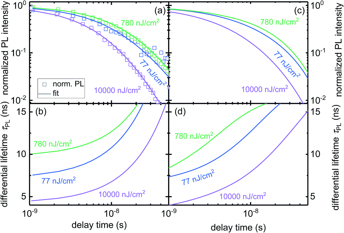 | ||
| Fig. 3 PL transients of a perovskite/PC61BM heterojunction. (a) Experimental data and fit (b) differential lifetime calculated from PL with eqn (4). See ESI Fig. S6† for data and fit. (c and d) Simulation, with a transfer velocity of ST = 5.3 × 103 cm s−1 and an interface-recombination velocity of SR = 200 cm s−1. | ||
Fig. 3c and d present the result of the best fitting simulations with an interface-recombination velocity SR = 200 cm s−1 and a transfer velocity of ST = 5.3 × 103 cm s−1 showing a good agreement with the experimental data in Fig. 3a and b. The increase of lifetime between lowest to medium light intensity can be explained by the accumulation of charges at the interface, which repel further electrons from the bulk, slowing down charge transfer while increasing the differential lifetime. For the highest laser intensity an additional effect starts to impact the PL because a laser intensity of 10000 nJ cm−2 generates a high number of charge carriers and therefore higher order recombination mechanisms (radiative and Auger recombination) become relevant and decrease the differential lifetime (see Fig. S7b†).
In order to identify, whether the obtained best-fit parameters are likely a unique solution, we simulated the differential lifetime for several cases taking into account the first 50 ns of the decay and varying the transfer and the interface recombination velocities. Fig. 4a and b shows how much the results from these simulations deviate from the results of the best fitting parameter set (as seen in Fig. 3d) for 77 nJ cm−2 and 780 nJ cm−2, respectively. Fig. 4a shows an area with low values spanning over several orders of magnitude of the interfacial recombination velocity SR indicating that a similar result as shown in Fig. 3d (77 nJ cm−2) could be recreated with other parameter sets. This effect occurs because the transfer rate is more independent of the recombination velocity at low fluences. Fig. 4b shows low errors (≙ good fits) at several combinations of recombination and transfer velocities because high recombination velocities can lower the accumulation and thereby increase the transfer rate, making it possible to recreate a similar curve with different parameter sets. However, the combination of the error calculated for both laser fluences (Fig. 4c) shows a smaller area of low errors indicating that a result which simultaneously fits both curves cannot be recreated with different parameter sets when using more than one laser fluence. Hence, several laser fluxes are needed to achieve an unambiguous result.
 | ||
| Fig. 4 Examining if different transfer and recombination velocities can lead to similar results as in Fig. 3d. Larger areas of low values and therefore similar curves exist for EL = 77 nJ cm−2 (a) and EL = 780 nJ cm−2 (b). (c) Combination of (a) and (b). Parameter sets where both curves are similar to Fig. 3d at the same time exist only in near vicinity of the best fitting parameter SR = 200 cm s−1 and ST = 5321 cm s−1. Data points have been interpolated for a smoother image. | ||
5. Conclusions and outlook
We conclude that analyzing PL transients with numerical simulations provides us with an enhanced understanding of the dominating processes. We show that the accumulation of charge carriers at the interface, which is neglected in analytical equations, has a major impact on the results. Carefully analyzing and comparing experimental results from a sample with simulations gives us an estimate for the parameters that determine transfer and interfacial recombination. Further investigation of these parameters shows that they are not entirely independent from each other because of the interactions of transfer and recombination, but we can still determine the surface recombination velocity at the perovskite/PC61BM interface precisely if more than one laser fluence is used.Our current model system uses an electron-transport layer like PC61BM that achieves hole-blocking properties by band offsets rather than by creating band bending, in order to minimize effects of ion movement on the transients and to reduce the free parameters for the simulations. In the next steps we need to extend the model to interfaces like TiO2/perovskite or PEDOT:PSS/perovskite, where the contact layers are doped and where ion movement and its influence on electric field distributions would have to be considered.
6. Experimental section
Numerical simulations
We modeled the transient photoluminescence of the perovskite/PC61BM heterojunction with Synopsys TCAD Sentaurus (Version J-2014.09) in 1D assuming layer thicknesses of 300 nm and 100 nm for the perovskite and the quencher layers, respectively. The software solves the time-dependent continuity equations for electrons and holes as well as the Poisson equation. See ref. 7–10 and 56 for further details on drift-diffusion simulations. Simulation parameters are presented in Table S1† and the complex refractive indices used are shown in Fig. S2a and S2b.†To take reabsorption in the perovskite layer into account we obtained the radiative recombination rate Rrad from the simulation results and calculated the photon rate per energy at all locations in the cell. The photon rate enables us to calculate the reabsorption according to the Lambert–Beer law (for more details see ESI†). For implementation of interfacial recombination we inserted a 0.1 nm thin interlayer with high SRH recombination into the simulation, with the interlayer having the same electron affinity as the quencher layer and the interlayer valance band having the same energetic level as the bulk valance band. The interface-recombination velocity effectively caused by this interlayer can be calculated by SR = dint/τint, with dint being the thickness and τint the SRH-lifetime of the interlayer.
Sample fabrication
The CH3NH3PbI3/PC61BM heterojunctions were fabricated on 12 × 12 mm Corning glass substrates. The perovskite layer (thickness: 311 ± 10 nm) was spin-coated from a solution of lead chloride (PbCl2) and methylammonium iodide (MAI) in dimethylformamide (molar ratio MAI:PbCl2 = 3:1 (35 wt%)) at 3000 rpm for 35 s with a ramp time of 10 s. The samples were annealed for 140 min at 90 °C on a hot plate (ambient air, 36% relative humidity) and a PC61BM layer (thickness: 80 ± 10 nm) was spin-coated at 1500 rpm for 60 s with a ramp time of 5 s on top of the perovskite from 50 μl of a 20 mg ml−1 PC61BM/chlorobenzene solution.
Transient PL measurements
A 496 nm laser pulse hit the sample with a beam diameter of approximately 800 μm in an angle of 30° from the glass side for approximately 1 ns (FWHM). Laser fluences were adjusted with neutral density filters and measured with a calibrated, fast Si photodiode (J-10SI-HE from Coherent). The spectrum of the PL was resolved by a SPEX 270M monochromator from Horiba Jobin Yvon and subsequently detected by a gated ICCD camera (iStar DH720 from Andor Solis). The gate of the camera is kept open for 2 to 8 ns depending on the PL signal strength. After the measurement the spectrum was integrated over photon energy to get the total photon count and normalized to the maximum value.Conflicts of interest
There are no conflicts of interest to declare.Acknowledgements
The authors acknowledge support from the Deutsche Forschungsgemeinschaft (Grants No. KI-1571/2-1 and RA-473/7-1) and from the Bavarian Ministry for Economics, Media, Energy and Technology via the project “Perowskit basierte Tandem-Solarzellen”.References
- R. K. Ahrenkiel, in Semiconductors and Semimetals, ed. R. K. Ahrenkiel and M. S. Lundstrom, Elsevier, Amsterdam, 1993, vol. 39, pp. 39–150 Search PubMed.
- R. M. Sieg, J. A. Carlin, J. J. Boeckl, S. A. Ringel, M. T. Currie, S. M. Ting, T. A. Langdo, G. Taraschi, E. A. Fitzgerald and B. M. Keyes, Appl. Phys. Lett., 1998, 73, 3111–3113 CrossRef CAS.
- G. Wang, S. Fafard, D. Leonard, J. E. Bowers, J. L. Merz and P. M. Petroff, Appl. Phys. Lett., 1994, 64, 2815–2817 CrossRef CAS.
- W. K. Metzger, I. L. Repins and M. A. Contreras, Appl. Phys. Lett., 2008, 93, 022110 CrossRef.
- S. Shimakawa, K. Kitani, S. Hayashi, T. Satoh, Y. Hashimoto, Y. Takahashi and T. Negami, Phys. Status Solidi, 2006, 203, 2630–2633 CrossRef CAS.
- S. Shirakata and T. Nakada, Thin Solid Films, 2007, 515, 6151–6154 CrossRef CAS.
- M. Maiberg and R. Scheer, J. Appl. Phys., 2014, 116, 123710 CrossRef.
- M. Maiberg and R. Scheer, J. Appl. Phys., 2014, 116, 123711 CrossRef.
- M. Maiberg, T. Hölscher, S. Zahedi-Azad and R. Scheer, J. Appl. Phys., 2015, 118, 105701 CrossRef.
- M. Maiberg, F. Bertram, M. Müller and R. Scheer, J. Appl. Phys., 2017, 121, 085703 CrossRef.
- A. Redinger, S. Levcenko, C. J. Hages, D. Greiner, C. A. Kaufmann and T. Unold, Appl. Phys. Lett., 2017, 110, 122104 CrossRef.
- W. K. Metzger, D. Albin, D. Levi, P. Sheldon, X. Li, B. M. Keyes and R. K. Ahrenkiel, J. Appl. Phys., 2003, 94, 3549–3555 CrossRef CAS.
- X. Wu, Sol. Energy, 2004, 77, 803–814 CrossRef CAS.
- A. Kanevce, D. H. Levi and D. Kuciauskas, Prog. Photovoltaics, 2014, 22, 1138–1146 CAS.
- D. Kuciauskas, I. Repins, A. Kanevce, J. V. Li, P. Dippo and C. L. Beall, Sol. Energy Mater. Sol. Cells, 2015, 136, 100–105 CrossRef CAS.
- C. J. Hages, A. Redinger, S. Levcenko, H. Hempel, M. J. Koeper, R. Agrawal, D. Greiner, C. A. Kaufmann and T. Unold, Adv. Energy Mater., 2017, 7, 1700167 CrossRef.
- S. D. Stranks, G. E. Eperon, G. Grancini, C. Menelaou, M. J. P. Alcocer, T. Leijtens, L. M. Herz, A. Petrozza and H. J. Snaith, Science, 2013, 342, 341–344 CrossRef CAS PubMed.
- Y. Yamada, T. Nakamura, M. Endo, A. Wakamiya and Y. Kanemitsu, J. Am. Chem. Soc., 2014, 136, 11610–11613 CrossRef CAS PubMed.
- D. Shi, V. Adinolfi, R. Comin, M. Yuan, E. Alarousu, A. Buin, Y. Chen, S. Hoogland, A. Rothenberger, K. Katsiev, Y. Losovyj, X. Zhang, P. A. Dowben, O. F. Mohammed, E. H. Sargent and O. M. Bakr, Science, 2015, 347, 519–522 CrossRef CAS PubMed.
- F. Staub, H. Hempel, J.-C. Hebig, J. Mock, U. W. Paetzold, U. Rau, T. Unold and T. Kirchartz, Phys. Rev. Appl., 2016, 6, 044017 CrossRef.
- D. W. de Quilettes, S. M. Vorpahl, S. D. Stranks, H. Nagaoka, G. E. Eperon, M. E. Ziffer, H. J. Snaith and D. S. Ginger, Science, 2015, 348, 683–686 CrossRef CAS PubMed.
- D. Guo, D. Bartesaghi, H. Wei, E. M. Hutter, J. Huang and T. J. Savenije, J. Phys. Chem. Lett., 2017, 8, 4258–4263 CrossRef CAS PubMed.
- G. Xing, N. Mathews, S. S. Lim, N. Yantara, X. Liu, D. Sabba, M. Grätzel, S. Mhaisalkar and T. C. Sum, Nat. Mater., 2014, 13, 476–480 CrossRef CAS PubMed.
- X. Zhang, Z. Li, Y. Ding, L. Hu, J. Ye, X. Pan and S. Dai, Sustainable Energy Fuels, 2017, 1, 1056–1064 CAS.
- J. Nelson, in Physics of Solar Cells, 2003, pp. 79–117 Search PubMed.
- E. Edri, S. Kirmayer, S. Mukhopadhyay, K. Gartsman, G. Hodes and D. Cahen, Nat. Commun., 2014, 5, 3461 CrossRef PubMed.
- V. Sarritzu, N. Sestu, D. Marongiu, X. Chang, S. Masi, A. Rizzo, S. Colella, F. Quochi, M. Saba, A. Mura and G. Bongiovanni, Sci. Rep., 2017, 7, 44629 CrossRef CAS PubMed.
- J.-P. Correa-Baena, S.-H. Turren-Cruz, W. Tress, A. Hagfeldt, C. Aranda, L. Shooshtari, J. Bisquert and A. Guerrero, ACS Energy Lett., 2017, 2, 681–688 CrossRef CAS.
- I. Zarazua, G. Han, P. P. Boix, S. Mhaisalkar, F. Fabregat-Santiago, I. Mora-Seró, J. Bisquert and G. Garcia-Belmonte, J. Phys. Chem. Lett., 2016, 7, 5105–5113 CrossRef CAS PubMed.
- Y. Yang, M. Yang, D. T. Moore, Y. Yan, E. M. Miller, K. Zhu and M. C. Beard, Nat. Energy, 2017, 2, 16207 CrossRef CAS.
- Q. Wang, Q. Dong, T. Li, A. Gruverman and J. Huang, Adv. Mater., 2016, 28, 6734–6739 CrossRef CAS PubMed.
- Y. Lin, L. Shen, J. Dai, Y. Deng, Y. Wu, Y. Bai, X. Zheng, J. Wang, Y. Fang, H. Wei, W. Ma, X. C. Zeng, X. Zhan and J. Huang, Adv. Mater., 2017, 29, 1604545 CrossRef PubMed.
- X. Zheng, B. Chen, J. Dai, Y. Fang, Y. Bai, Y. Lin, H. Wei, X. C. Zeng and J. Huang, Nat. Energy, 2017, 2, 17102 CrossRef CAS.
- M. T. Masood, C. Weinberger, J. Sarfraz, E. Rosqvist, S. Sandén, O. J. Sandberg, P. Vivo, G. Hashmi, P. D. Lund, R. Österbacka and J. H. Smatt, ACS Appl. Mater. Interfaces, 2017, 9, 17906–17913 CAS.
- F. X. Xie, H. Su, J. Mao, K. S. Wong and W. C. H. Choy, J. Phys. Chem. C, 2016, 120, 21248–21253 CAS.
- Q. Chen, H. Zhou, Y. Fang, A. Z. Stieg, T.-B. Song, H.-H. Wang, X. Xu, Y. Liu, S. Lu, J. You, P. Sun, J. McKay, M. S. Goorsky and Y. Yang, Nat. Commun., 2015, 6, 7269 CrossRef CAS PubMed.
- G. Xing, N. Mathews, S. Sun, S. S. Lim, Y. M. Lam, M. Gratzel, S. Mhaisalkar and T. C. Sum, Science, 2013, 342, 344–347 CrossRef CAS PubMed.
- K. Pydzińska, J. Karolczak, I. Kosta, R. Tena-Zaera, A. Todinova, J. Idígoras, J. A. Anta and M. Ziółek, ChemSusChem, 2016, 9, 1647–1659 CrossRef PubMed.
- S. Makuta, M. Liu, M. Endo, H. Nishimura, A. Wakamiya and Y. Tachibana, Chem. Commun., 2016, 52, 673–676 RSC.
- P. Piatkowski, B. Cohen, F. Javier Ramos, M. Di Nunzio, M. K. Nazeeruddin, M. Grätzel, S. Ahmad and A. Douhal, Phys. Chem. Chem. Phys., 2015, 17, 14674–14684 RSC.
- J. C. Brauer, Y. H. Lee, M. K. Nazeeruddin and N. Banerji, J. Mater. Chem. C, 2016, 4, 5922–5931 RSC.
- B. Wu, K. Fu, N. Yantara, G. Xing, S. Sun, T. C. Sum and N. Mathews, Adv. Energy Mater., 2015, 5, 1500829 CrossRef.
- L. Kegelmann, C. M. Wolff, C. Awino, F. Lang, E. L. Unger, L. Korte, T. Dittrich, D. Neher, B. Rech and S. Albrecht, ACS Appl. Mater. Interfaces, 2017, 9, 17245–17255 CAS.
- H.-S. Rao, B.-X. Chen, X.-D. Wang, D.-B. Kuang and C.-Y. Su, Chem. Commun., 2017, 53, 5163–5166 RSC.
- C. Roldán-Carmona, P. Gratia, I. Zimmermann, G. Grancini, P. Gao, M. Graetzel and M. K. Nazeeruddin, Energy Environ. Sci., 2015, 8, 3550–3556 Search PubMed.
- J. Xie, X. Yu, J. Huang, X. Sun, Y. Zhang, Z. Yang, M. Lei, L. Xu, Z. Tang, C. Cui, P. Wang and D. Yang, Adv. Sci., 2017, 4, 1700018 CrossRef PubMed.
- M. Zhang, J. Wang, L. Li, G. Zheng, K. Liu, M. Qin, H. Zhou and X. Zhan, Adv. Sci., 2017, 4, 1700025 CrossRef PubMed.
- A. E. Shalan, S. Narra, T. Oshikiri, K. Ueno, X. Shi, H.-P. Wu, M. M. Elshanawany, E. Wei-Guang Diau and H. Misawa, Sustainable Energy Fuels, 2017, 1, 1533–1540 CAS.
- C. S. Ponseca, E. M. Hutter, P. Piatkowski, B. Cohen, T. Pascher, A. Douhal, A. Yartsev, V. Sundström and T. J. Savenije, J. Am. Chem. Soc., 2015, 137, 16043–16048 CrossRef CAS PubMed.
- E. M. Hutter, J.-J. Hofman, M. L. Petrus, M. Moes, R. D. Abellon, P. Docampo and T. J. Savenije, Adv. Energy Mater., 2017, 7, 1602349 CrossRef.
- C. M. Wolff, F. Zu, A. Paulke, L. P. Toro, N. Koch and D. Neher, Adv. Mater., 2017, 29, 1700159 CrossRef PubMed.
- S. Shao, M. Abdu-Aguye, L. Qiu, L.-H. Lai, J. Liu, S. Adjokatse, F. Jahani, M. E. Kamminga, G. H. ten Brink, T. T. M. Palstra, B. J. Kooi, J. C. Hummelen and M. Antonietta Loi, Energy Environ. Sci., 2016, 9, 2444–2452 CAS.
- L. G. Kudriashova, D. Kiermasch, P. Rieder, M. Campbell, K. Tvingstedt, A. Baumann, G. V. Astakhov and V. Dyakonov, J. Phys. Chem. Lett., 2017, 8, 4698–4703 CrossRef CAS PubMed.
- M. Burgelman, P. Nollet and S. Degrave, Thin Solid Films, 2000, 361–362, 527–532 CrossRef CAS.
- B. E. Pieters, K. Decock, M. Burgelman, R. Stangl and T. Kirchartz, in Advanced Characterization Techniques for Thin Film Solar Cells, ed. D. Abou-Ras, T. Kirchartz and U. Rau, Wiley-VCH Verlag GmbH & Co. KGaA, Weinheim, Germany, 2nd edn, 2016, vol. 2, pp. 633–657 Search PubMed.
- A. Kanevce and W. K. Metzger, in Advanced Characterization Techniques for Thin Film Solar Cells, ed. D. Abou-Ras, T. Kirchartz and U. Rau, Wiley-VCH Verlag GmbH & Co. KGaA, Weinheim, Germany, 2nd edn, 2016, vol. 2, pp. 659–674 Search PubMed.
- A. Gagliardi and A. Abate, ACS Energy Lett., 2018, 3, 163–169 CrossRef CAS.
- P. Calado, A. M. Telford, D. Bryant, X. Li, J. Nelson, B. C. O'Regan and P. R. F. Barnes, Nat. Commun., 2016, 7, 13831 CrossRef CAS PubMed.
- I. Zonno, B. Krogmeier, V. Katte, D. Lübke, A. Martinez-Otero and T. Kirchartz, Appl. Phys. Lett., 2016, 109, 183301 CrossRef.
- I. Zonno, A. Martinez-Otero, J.-C. Hebig and T. Kirchartz, Phys. Rev. Appl., 2017, 7, 034018 CrossRef.
- W. K. Metzger, I. L. Repins, M. Romero, P. Dippo, M. Contreras, R. Noufi and D. Levi, Thin Solid Films, 2009, 517, 2360–2364 CrossRef CAS.
- D. Schroeder, in Modelling of Interface Carrier Transport for Device Simulation, Springer Vienna, Vienna, 1994, pp. 154–171 Search PubMed.
- Synopsys, in Sentaurus™ Device User Guide J-2014.09, Mountain View, CA, 2014, pp. 716–717 Search PubMed.
- R. Brendel and R. Peibst, IEEE Journal of Photovoltaics, 2016, 6, 1413–1420 CrossRef.
- A. Spies, M. List, T. Sarkar and U. Würfel, Adv. Energy Mater., 2017, 7, 1601750 CrossRef.
- U. Würfel, A. Cuevas and P. Würfel, IEEE Journal of Photovoltaics, 2015, 5, 461–469 CrossRef.
- O. J. Sandberg, A. Sundqvist, M. Nyman and R. Österbacka, Phys. Rev. Appl., 2016, 5, 044005 CrossRef.
- T. Kirchartz, F. Staub and U. Rau, ACS Energy Lett., 2016, 1, 731–739 CrossRef CAS.
- M. A. Faist, T. Kirchartz, W. Gong, R. S. Ashraf, I. McCulloch, J. C. de Mello, N. J. Ekins-Daukes, D. D. C. Bradley and J. Nelson, J. Am. Chem. Soc., 2012, 134, 685–692 CrossRef CAS PubMed.
- F. Staub, T. Kirchartz, K. Bittkau and U. Rau, J. Phys. Chem. Lett., 2017, 8, 5084–5090 CrossRef CAS PubMed.
Footnote |
| † Electronic supplementary information (ESI) available. See DOI: 10.1039/c7se00603a |
| This journal is © The Royal Society of Chemistry 2018 |