
Performance and failure modes of Si anodes patterned with thin-film Ni catalyst islands for water oxidation†
Ke
Sun
 a,
Nicole L.
Ritzert
bc,
Jimmy
John
a,
Haiyan
Tan
bc,
William G.
Hale
d,
Jingjing
Jiang
e,
Ivan
Moreno-Hernandez
a,
Kimberly M.
Papadantonakis
a,
Thomas P.
Moffat
c,
Bruce S.
Brunschwig
f and
Nathan S.
Lewis
*af
a,
Nicole L.
Ritzert
bc,
Jimmy
John
a,
Haiyan
Tan
bc,
William G.
Hale
d,
Jingjing
Jiang
e,
Ivan
Moreno-Hernandez
a,
Kimberly M.
Papadantonakis
a,
Thomas P.
Moffat
c,
Bruce S.
Brunschwig
f and
Nathan S.
Lewis
*af
aDivision of Chemistry and Chemical Engineering, California Institute of Technology, 1200 E. California Blvd., Pasadena, CA 91125, USA. E-mail: nslewis@caltech.edu
bTheiss Research, 7411 Eads Ave., La Jolla, California 92037, USA
cNational Institute of Standards and Technology, Material Measurement Laboratory, 100 Bureau Dr., Gaithersburg, MD 20899, USA
dDepartment of Chemistry, University of Southampton, Southampton, Hampshire SO17 1BJ, UK
eDivision of Engineering and Applied Sciences, California Institute of Technology, 1200 E. California Blvd., Pasadena, CA 91125, USA
fBeckman Institute Molecular Materials Research Center, California Institute of Technology, Pasadena, 1200 E. California Blvd, CA 91125, USA
First published on 6th March 2018
Abstract
Silicon photoanodes patterned with thin-film Ni catalyst islands exhibited stable oxygen evolution for over 240 h of continuous operation in 1.0 mol L−1 KOH under simulated sunlight conditions. Buried-junction np+-Si(111) photoanodes with an 18.0% filling fraction of a square array of Ni microelectrodes, np+-Si(111)|NiμE18.0%, demonstrated performance equivalent to a Ni anode in series with a photovoltaic device having an open-circuit voltage of 538 ± 20 mV, a short-circuit current density of 20.4 ± 1.3 mA cm−2, and a photovoltaic efficiency of 6.7 ± 0.9%. For the np+-Si(111)|NiμE18.0% samples, the photocurrent density at the equilibrium potential for oxygen evolution was 12.7 ± 0.9 mA cm−2, yielding an ideal regenerative cell solar-to-oxygen conversion efficiency of 0.47 ± 0.07%. The photocurrent passed exclusively through the Ni catalyst islands to evolve O2 with nearly 100% faradaic efficiency, while a passivating, insulating surface layer of SiOx formed in situ on areas of the Si in direct contact with the electrolyte. The (photo)electrochemical behavior of Si electrodes patterned with varying areal filling fractions of Ni catalyst islands was also investigated. The stability and efficiency of the patterned-catalyst Si electrodes were affected by the filling fraction of the Ni catalyst, the orientation and dopant type of the substrates, and the measurement conditions. The electrochemical behavior at different stages of operation, including Ni catalyst activation, Si passivation, stable operation, and device failure, was affected by the dynamic processes of anodic formation and isotropic dissolution of SiOx on the exposed Si. Ex situ and operando microscopic and spectroscopic studies revealed that these processes were three-dimensional and spatially non-uniform across the surface of the substrate, and occurred near the active catalyst islands. The patterned catalyst/substrate electrodes serve as a model system for accelerated studies of failure mechanisms in photoanodes protected by multifunctional catalytic coatings or other hole-conductive thin-film coatings that contain defects.
Introduction
During the photoelectrochemical oxygen-evolution reaction (OER), small-band-gap (EG < 2 eV) semiconductor electrodes typically corrode rapidly in the presence of energetic holes, through thermodynamically favorable anodic decomposition reactions that compete with the kinetically difficult OER.1–3 Stabilization of such semiconductors under OER conditions constitutes an important enabling step in the development of a fully integrated solar-fuels device.4 Transparent catalyst films that form physical barriers between the electrolyte and small-band-gap semiconductors, specifically Si,5–22 have been used to protect Si photoanodes and produce stable operation for >1000 h under sunlight-driven oxygen-evolution conditions in alkaline media.23,24 For example, n-Si(100)/SiOx/CoOx photoanodes protected by multifunctional NiOx films have exhibited stable and efficient light-driven oxygen evolution for over 1200 h of continuous operation.23,24Pinhole and/or grain-boundary defects are common in thin, protective coatings, especially for films covering large substrate areas. Such defects can also develop if the catalyst films change composition and/or structure during deployment and operation. The stability of protected photoanodes in different electrochemical environments is controlled by the formation and confinement of insoluble oxides near defects.25–28 For example, Si, CdTe, and InP can be protected by defective NiOx films in 1.0 mol L−1 KOH,25,28,29 indicating that such photoanodes are defect tolerant under these operating conditions. In contrast, with nominally identical NiOx films, planar GaAs and InGaP electrodes exhibit catastrophic failure over comparable operating timescales.
Patterning of thin-film catalysts into protective oxide layers offers an alternative to transparent, conductive, catalytically active protective coatings for the stabilization of small-band-gap semiconducting photoanodes. In the patterned-catalyst approach, the geometry of the island array is designed to maximize light absorption in the underlying semiconductor while minimizing the resistance for charge collection and the catalytic overpotential. For example, np+-Si(100) photoanodes with thin-film islands of Pt or Ni patterned in a thermal SiOx layer have exhibited >24 h of stable, light-driven oxygen evolution in 1 mol L−1 NaOH.30 Also, n-Si(100) photoanodes protected by 30 nm of insulating SiOx that developed conducting channels due to oxide breakdown at high electric fields have exhibited 40 h of stability under light-driven oxygen evolution in 1.0 mol L−1 KOH.31 More recently, Ni nanoparticles dispersed on the surface of Si photoanodes have enabled stable operation for >40 h in 1 mol L−1 NaOH, with the exposed Si surface passivated by a SiOx layer that develops during operation.32,33
Although these demonstrations represent progress toward the realization of photoanodes that are stable under OER conditions, an understanding of how the chemical and physical structures of the catalyst, protective oxide layers, and semiconducting substrate change – both under OER conditions and while at rest in contact with the electrolyte – including the rate of such changes, and the effects of those changes on the performance of the devices, will be required to understand failure mechanisms and to establish commercially viable lifetimes on the order of decades. Experimental work of this type has begun to emerge recently, with one study showing that the aging of thin, optically transparent metallic Ni protective films on Si surfaces during OER results in conversion of the Ni film to ion-permeable Ni hydroxide/oxyhydroxide, presumably allowing a passive interfacial SiOx layer to form at the interface.27
Herein, the patterned-catalyst design is used to probe the surface of unstable photoanode materials at different interfaces and to examine the stability of the passivating layer, aiming to fill a knowledge gap in understanding the failure mechanisms in integrated photoelectrochemical devices under various conditions, and to shed light on future development of effective protection strategies and new system designs for integrated solar-fuel devices. Various microscopic and spectroscopic techniques have been used in conjunction with electrochemistry to investigate the performance and durability of an exemplary system, micrometer-sized Ni OER island electrodes, NiμEs, on Si. Non-photoactive p+-Si(111)|NiμEs have been used to evaluate the catalyst stability as well as the formation of passivating SiOx under dark conditions. Our effort focused on Si(111) surfaces because they are more resistant to corrosion in alkaline media than either Si(100) or Si(110) surfaces.22 The impact of the diurnal cycle on the electrode stability was evaluated by investigating the behavior of catalyst-patterned Si(100) substrates under open-circuit conditions in contact with alkaline aqueous electrolytes.
Experimental
Chemicals
All chemicals, including sulfuric acid (H2SO4, J. T. Baker, Tewksbury, MA., ACS reagent, 95–98%), concentrated hydrochloric acid (HCl, Sigma Aldrich, St. Luis, MO., ACS Reagent 37%), hydrogen peroxide (H2O2, Macron Chemicals, Center Valley, PA., ACS grade 30%), concentrated ammonium hydroxide (NH4OH, Sigma Aldrich, St. Luis, MO. ACS reagent 28–30%), buffered hydrofluoric acid improved (Transene Company Inc., Danvers, MA.), potassium hydroxide pellets (KOH, Macron Chemicals, Center Valley, PA., ACS 88%), sodium hydroxide (NaOH, Sigma Aldrich, St. Luis, MO., ACS reagent), potassium ferrocyanide trihydrate (K4Fe(CN)6·3H2O, Acros, St. Luis, MO., >99%), potassium ferricyanide (K3Fe(CN)6, Fisher Chemicals, Tewksbury, MA., certified ACS 99.4%), and potassium chloride (KCl, Macron Chemicals, Center Valley, PA., Granular ACS 99.6%), were used as received. Commercial materials and equipment are identified in this paper to specify adequately the experimental procedure. In no case does such identification imply recommendation or endorsement by the National Institute of Standards and Technology, nor does it necessarily imply that the product is the best available for the purpose. Water with a resistivity of 18.2 MΩ cm was obtained from a Millipore deionized (DI) water system.Sample preparation and patterning and deposition of microelectrode (μE) arrays
Degenerately boron-doped (p+-type, resistivity <0.005 ohm cm, single-side polished, (111) or (100) oriented, 4° miscut) or phosphorus-doped (n-type, resistivity 0.5–1 ohm cm, single-side polished, (111) oriented, 4° miscut) Si wafers were purchased from Addison Engineering. Room-temperature ion implantation was performed on n-Si at a 7° incident angle using 11B accelerated to 45 keV with a dose of 1 × 1014 cm−2, and then at 32 keV with a dose of 5 × 1014 cm−2. To reduce the contact resistance, the back sides of the wafers were implanted with 31P at 140 keV with a dose of 1 × 1014 cm−2, and then at 75 keV with a dose of 5 × 1014 cm−2. Dopant activation, both for the junction p+ layer and the n+ back-surface field (BSF) layer, was achieved by rapid thermal annealing at 1000 °C for 15 s under a flow of N2.Ni catalyst microelectrodes, NiμEs, with diameters of 5 μm or 10 μm were patterned in square arrays on Si substrates using a standard lift-off photolithography procedure. Four arrays were patterned with Ni areal filling fractions of 1.0, 6.2, 18.0 or 35.7% on the Si electrodes by changing the pitch of the microelectrode pattern. A coverage of 100% refers to a complete Ni thin film.
Bare Si wafers were cleaned by immersion in 1![[thin space (1/6-em)]](https://www.rsc.org/images/entities/char_2009.gif) :1:5 H2O2:NH4OH:H2O (by volume) at 70 °C for 30 min, followed by buffered oxide etchant, typically for 30 s to 45 s, until the surface became hydrophobic, and then 1:1:5 H2O2:HCl:H2O (by volume) at 70 °C for 30 min. The wafers were then thoroughly rinsed using deionized H2O and were dried under a stream of N2.
:1:5 H2O2:NH4OH:H2O (by volume) at 70 °C for 30 min, followed by buffered oxide etchant, typically for 30 s to 45 s, until the surface became hydrophobic, and then 1:1:5 H2O2:HCl:H2O (by volume) at 70 °C for 30 min. The wafers were then thoroughly rinsed using deionized H2O and were dried under a stream of N2.
Before deposition of Ni, bare or photoresist-patterned Si samples were immersed in a buffered oxide etching solution for 30 s to 45 s, until the exposed Si became hydrophobic. Samples were quickly rinsed using deionized H2O, dried using N2, and promptly transferred to a sputtering chamber that had a typical base pressure of 5 × 10⁻⁸ Torr. Between 1 and 30 nm of Ni was sputter-deposited on p+-Si for studies, including electrochemical activity, faradaic efficiency, short-term stability, optical absorption, etc. These films were deposited without substrate heating, while the sample was under an Ar flow of 20 sccm to maintain a working pressure of 5 mTorr. Initial studies were conducted using unpatterned Ni films with thicknesses in the range of 1–30 nm on p+-Si substrates to gauge the effects of the Ni thickness on electrochemical measurements and to determine the minimum thickness required for electrochemical and electrocatalytic behavior and minimal resistance losses. For photoresist-patterned samples, after lift-off the samples were then rinsed with acetone followed by an isopropanol rinse, and were dried with N2 before being assembled into electrodes. Si|NiμEs were all patterned with 15 nm thick Ni films, unless stated otherwise. A thick Ni loading (∼100 nm) was used on np+-Si and n-Si photoanodes in long-term stability and failure-mode studies. The samples with thick Ni loadings for stability and failure-mode studies were annealed in vacuum at 300 °C for 45 min to improve the adhesion between the thick metal islands and the Si substrate.
Electrode preparation
Ohmic contacts were formed by scribing an In–Ga eutectic alloy (Alfa Aesar, 99.99%) to the back side of each Si sample. High-purity Ag paint (SPI supplies) was then used to mechanically attach the ohmic contact to a coiled, tin-plated Cu wire threaded through a glass tube. The sample was encapsulated and sealed to the glass tube using a 2:1 mixture of grey epoxy (Hysol 9460F) and white epoxy (Hysol 1C). The epoxy was allowed to dry under ambient conditions for >12 h. A high-resolution optical scanner (Epson perfection V370) with a resolution of 2400 dpi was used to image the exposed surface area of each electrode, and the geometric areas were determined by analyzing the images using ImageJ software.34 All of the electrodes used in this study were 0.1–0.2 cm2 in area, unless specified otherwise.
Activation of the electrode consisted of 10 cyclic voltammetry (CV) cycles between the rest potential, Eoc, and +1.93 V versus a reversible hydrogen electrode (RHE). During the 10 CVs, the catalytic activity of the Ni typically initially increased and then stabilized.35
Photoelectrochemical, spectral response, and faradaic efficiency measurements
A mercury/mercury oxide (Hg/HgO in 1.0 mol L−1 KOH) electrode was used as the reference electrode, and a Pt mesh in a fritted glass gas-dispersion tube was used as the counter electrode for photoelectrochemical, spectral response, and faradaic efficiency measurements. The Hg/HgO reference electrode was calibrated versus the RHE, with the Hg/HgO electrode potential determined to be 0.926 V vs. RHE. The equilibrium potential for the OER was 0.304 V versus the Hg/HgO reference in 1.0 mol L−1 KOH. A custom electrochemical cell with a flat glass (Pyrex) bottom was used for photoelectrochemical, spectral response, and faradaic efficiency measurements. During measurements, the electrolyte was stirred with a magnetic stir bar. The data were not compensated for any series resistance. Long-term stability tests were performed using ELH- or ENH-type (EIKO) tungsten-halogen lamps with a custom housing. A Xe arc lamp (Newport 67005 and 69911) equipped with an IR filter (Newport 61945) and with an Air Mass (AM) 1.5 filter (Newport 81094 and 71260) was used as the light source for electrochemical measurements. Further details of the electrochemical measurements have been provided previously25 and are illustrated in Fig. S5a.†Cyclic voltammograms, current density versus potential (J–E) data, and external quantum yield (Φext) data were obtained using a Biologic SP-200 potentiostat (Bio-Logic). J–E scans were recorded at a 40 mV s−1 scan rate. Unless specifically stated, J used in this work represents the current density normalized to the geometric surface area of the electrode. Jcat is used to represent the current density normalized to the geometric surface area of the catalyst islands on the electrode, thus Jcat is equal to J divided by the filling fraction of the catalyst islands. The potential-scan range varied depending on the photovoltage and the rest potential of the sample. The external quantum yield was measured with monochromatic light chopped at 20 Hz.
Samples for atomic-force microscopy (AFM), scanning-electron microscopy (SEM), transmission-electron microscopy (TEM), and X-ray photoelectron spectroscopy (XPS) were prepared electrochemically in a custom compression cell that had an exposed area of 0.27 cm2. To prepare samples for these studies, a peristaltic circulation pump was used to effectively remove bubbles by flushing solution onto the up-facing sample surface. To form ohmic contacts, Ni foil control samples and p+-Si(111)|NiμE0–100% samples were affixed to a glass slide using double-sided Cu tape. The back side of the p+-Si(111) samples was scratched with In–Ga eutectic and attached to the Cu tape by use of Ag paste. After measurement, p+-Si(111)|NiμE0–100% samples were thoroughly rinsed with deionized H2O and dried under a flow of N2.
Faradaic efficiency determination
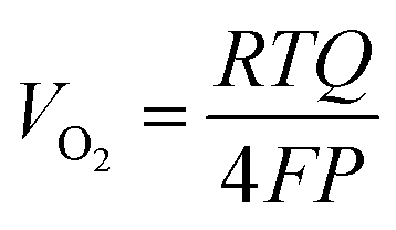
Faradaic efficiency measurements based on collection of evolved O2 were performed in 1.0 mol L−1 KOH using a custom eudiometer consisting of an inverted burette connected to a three-necked electrochemical cell, in the two-compartment electrochemical apparatus configured as described above.28 The 1.0 mol L−1 KOH electrolyte was first saturated with hydrated high-purity O2 for 2 h prior to the measurement. The measurements were performed galvanostatically at a current density of 10 mA cm−2 with electrodes that had relatively large (∼0.5 cm−2) surface areas, to enhance the gas-collection efficiency into the inverted burette. The p+-Si(111)|NiμE0–100% samples were not preactivated by cycling the potential before the collection of O2. The experiment setup is illustrated in Fig. S6a.†The faradaic efficiency was calculated as the ratio of the measured to the expected O2 volume. The expected volume, VO2 in units of mL, of generated O2 was calculated based on the charge, Q in units of coulombs, passed using a modified version of the ideal gas law equation:
 | (1) |
Scanning electrochemical microscopy (SECM)
SECM measurements were performed on three p+-Si(111)|NiμE1.0% electrodes with 10 μm diameter Ni catalyst islands using a model 920D scanning electrochemical microscope (CH Instruments, Austin, TX, USA) with Pt tip electrodes of 10 μm diameter. A Ni filling fraction of 1.0% was used to minimize overlap of the NiμE diffusion layers. Cu tape provided contact to the back of the sample via In–Ga eutectic (vide supra). The sample was mounted in a 2 mL PTFE (polytetrafluoroethylene) cell, and the area exposed to solution (0.28 or 0.50 cm2) was defined with an O-ring. The cell was wrapped with a paraffin film that contained holes to accommodate the electrodes. Solutions were de-aerated by bubbling the solution with N2 for >10 min, and images were collected under a blanket of N2. A coiled piece of Pt wire was used as the counter electrode. The error in positioning the tip was ±1 μm. The reference electrode was a Ag/AgCl/1 mol L−1 KCl electrode (+0.22 V vs. SHE;36 +1.05 V vs. RHE at pH 14.0) housed inside a salt bridge containing 3 g L−1 agar (ash 2.5% to 4.5%, Sigma Aldrich, St. Louis, MO) with 0.2 mol L−1 KNO3 (Alfa Aesar, Tewksbury, MA, 99.0%). The potential axis of the displayed data was subsequently adjusted to report potentials with respect to the RHE.Electrode characterization
The optical absorption of Si(111)NiμE samples was determined using an integrating sphere at normal incidence (Agilent Cary 5000 UV-vis spectrometer). The absorbance of p+-Si(111)|NiμE was determined by subtracting the measured reflectance and transmittance from unity. Diameters of the NiμEs and the surface morphology of the Ni and Si before and after electrochemical measurements were measured using a calibrated Nova NanoSEM 450 (FEI) SEM with an accelerating voltage of 5 kV. X-ray photoelectron spectroscopy (XPS) was performed using a Kratos AXIS Ultra DLD. High-resolution transmission-electron microscopy (TEM) was used to examine cross-sectioned p+-Si(111)|NiμE. The TEM lamella was prepared by focused ion-beam (FIB) milling (FEI Nova 600 NanoLab) using a pre-coating of C and Pt to protect the Ni island surface against ion damage. The lamella was thinned by 30 kV Ga ions for electron transparency and finished by 2 kV Ga ions to preserve the original state of the lamella. This sample-preparation technique is widely applied to semiconductors and other materials, resulting in typical final lamellae with a thickness <100 nm.37 TEM and scanning TEM (STEM) were performed at 300 keV using a probe-corrected FEI Titan 80–300 microscope. The inner and outer collection angles for HAADF-STEM were 70 mrad and 400 mrad, respectively. Energy-dispersive X-ray spectroscopy (XEDS) spectral images were collected by an Octane T Optima system from EDAX, which provides a windowless detector with solid angles up to 0.5 sr. In conjunction with STEM, site-specific electron energy-loss spectroscopy was performed on a Gatan GIF Tridiem spectrometer.Results
Structure and photoelectrochemical performance of p+-Si and np+-Si electrodes with Ni islands
SEM images of the Si|NiμE samples indicated that the Ni islands had diameters of 5.6 ± 0.1 μm and were positioned at pitches that produced surface coverages of 1.0 ± 0.1%, 6.2 ± 0.2%, 18.0 ± 0.9%, and 35.7 ± 1.6%, respectively (Fig. 1a). Fig. 1b–d show cross-sectional TEM and STEM images of p+-Si(111)|NiμE35.7% after 50 voltammetric cycles between +0.60 V and +2.15 V vs. RHE at 40 mV s−1 in 0.88 mol L−1 KOH under ambient conditions. The Ni island in the image was 145.6 nm thick at the center and 61.5 nm thick near the perimeter, presumably due to shadowing by the thick photoresist (∼3 μm) during sputtering (Fig. 1b). Some build-up of Ni along the sidewall of the photoresist pattern also occurred (Fig. 1c). A high-resolution cross-section TEM image of the interface between a Ni island and the Si(111) substrate showed that the Ni was polycrystalline with textured columnar grains, and exhibited a monotonic decrease in thickness and variation in orientation, evident towards the perimeter of the islands (Fig. 1d). The reaction between Ni and Si resulted in the formation of an 8 nm thick silicide layer. For Si(111), nickel silicides exhibit dominant epitaxial textures while on Si(100) more complex fiber textures are formed.38 In the present case, NiSi2 formation was observed, with the disilicide lattice being within 0.5% of the Si lattice. The resulting epitaxial relationship of NiSi2[1![[1 with combining macron]](https://www.rsc.org/images/entities/char_0031_0304.gif) 0]||Si[10] and NiSi2(111)||Si(111) was determined by diffraction and STEM imaging of the [112] and [110] zone axis (Fig. S1a†). The two possible orientations, type A and type B, share the surface normal but are rotated 180° with respect to one another and have different electrical barrier properties, Δ ∼0.1 eV, towards nondegenerately doped n-Si(111).39–41 Comparison of the electron-energy-loss spectra (EELS) of the Ni-L2,3 edge for the silicide and neighboring Ni layer revealed an ∼2 eV shift to higher energy, consistent with an increase in the oxidation state of Ni (Fig. S1b†), and in accord with previous reports for NiSi2.42 The silicide layer was separated from the Ni overlayer by a thin amorphous SiOx layer of variable thickness (Fig. 1c). The limited thickness of the oxide, along with silicide formation and degenerate doping of the p+-Si(111) substrate, ensured formation of a robust ohmic junction for this device.
0]||Si[10] and NiSi2(111)||Si(111) was determined by diffraction and STEM imaging of the [112] and [110] zone axis (Fig. S1a†). The two possible orientations, type A and type B, share the surface normal but are rotated 180° with respect to one another and have different electrical barrier properties, Δ ∼0.1 eV, towards nondegenerately doped n-Si(111).39–41 Comparison of the electron-energy-loss spectra (EELS) of the Ni-L2,3 edge for the silicide and neighboring Ni layer revealed an ∼2 eV shift to higher energy, consistent with an increase in the oxidation state of Ni (Fig. S1b†), and in accord with previous reports for NiSi2.42 The silicide layer was separated from the Ni overlayer by a thin amorphous SiOx layer of variable thickness (Fig. 1c). The limited thickness of the oxide, along with silicide formation and degenerate doping of the p+-Si(111) substrate, ensured formation of a robust ohmic junction for this device.
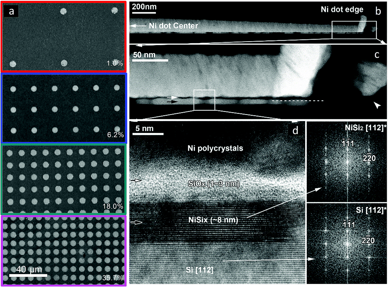 | ||
| Fig. 1 (a) SEM images of Si electrodes patterned with 5.6 μm diameter NiμE catalyst islands using filling fractions of 1.0–35.7%. (b) STEM image of a cross section of a p+-Si(111)|NiμE35.7% sample after 50 voltammetric cycles between +0.60 and +2.15 V vs. RHE in contact with 0.88 mol L−1 KOH. (c) STEM image of the cross-section at higher magnification showing the non-uniform SiOx and NiSix layer between the polycrystalline Ni and crystalline Si substrate. (d) High-resolution TEM image of the interface between a NiμE and the Si substrate and the fast Fourier transforms of the interfacial silicide and the Si(111) substrate. | ||
Fig. 2a shows representative J–E behavior of an np+-Si(111)|NiμE18.0% sample before (first cycle) and after (tenth cycle) activation under simulated Air Mass (AM) 1.5G illumination in 1.0 mol L−1 KOH. The J–E behavior of non-photoactive p+-Si(111)|NiμE18.0% is shown for comparison. A load-line analysis43 of the J–E behavior for the np+-Si(111)|NiμE18.0% yielded an open-circuit voltage, Voc, of 538 ± 20 mV, a short-circuit current density, Jsc, of 20.4 ± 1.3 mA cm−2, a fill factor, ff, of 61 ± 5%, and performance equivalent to a series-connected photovoltaic cell having an efficiency, ηPV, of 6.7 ± 0.9%. For the np+-Si(111)|NiμE18.0%, the photocurrent density at the formal potential for oxygen evolution, E0′(O2/H2O) = 1.229 V vs. RHE, was 12.7 ± 0.9 mA cm−2, yielding an ideal regenerative cell solar-to-O2 conversion efficiency,44ηIRC, of 0.47 ± 0.07%. Both np+- and p+-Si(111) showed hysteresis during the first voltammetric cycle. However, the hysteresis decreased with cycles and was minimal after 10 cycles. The shift in the J–E behavior with respect to the current onset is consistent with the Voc of the photovoltaic component extracted from the load-line analysis method.
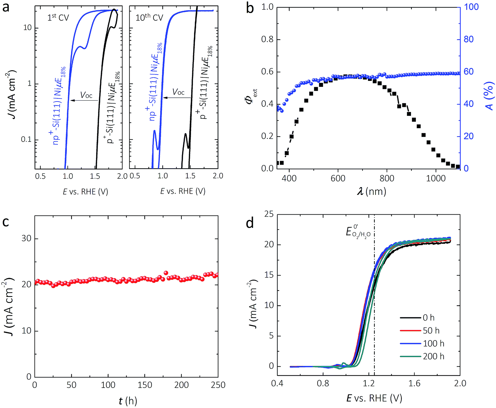 | ||
| Fig. 2 (a) Comparison of the current-density vs. potential (semi-log J–E) behavior for Si electrodes patterned with NiμEs at an 18.0% Ni filling fraction in 1.0 mol L−1 KOH. The first (left panel) and tenth (right panel) potential cycles are shown for np+-Si(111)|NiμE18.0% (blue curve) under simulated AM1.5G solar illumination. Non-photoactive p+-Si(111)|NiμE18.0% (black curve) is shown for comparison. (b) External quantum yield, Φext, from np+-Si(111)|NiμE18.0% poised at 1.73 V vs. RHE in 1.0 mol L−1 KOH (black squares) and the optical absorptance of a Si|NiμE18.0% in air (blue circles). (c) Chronoamperometric stability of an np+-Si(111)|NiμE18.0% photoelectrode at 1.73 V vs. RHE in 1.0 mol L−1 KOH under 100 mW cm−2 illumination from an ENH halogen lamp. (d) J–E behavior of np+-Si(111)|NiμE18.0% collected periodically during the stability test shown in (c). The scan rate was 40 mV s−1 for (a) and (d). | ||
Fig. 2b shows the external quantum yield, Φext, of the np+-Si(111)|NiμE18.0% electrode at +1.73 V vs. RHE. Φext was <0.6 across the entire visible spectrum, likely due to the broad reflectance of the bare Si in conjunction with the absorbance and reflectance of the Ni metal. Fig. S2a† shows the relationship between the Ni filling fraction and the absorptance of Si|NiμEs. Integration of Φext for the np+-Si(111)|NiμE18.0% photoanode with respect to the distribution of spectral irradiance of the AM 1.5G solar spectrum produced an expected light-limited photocurrent density of 20.4 mA cm−2, consistent with the J–E data at +1.73 V vs. RHE (Fig. 2a). Fig. S2b† shows the relationship between the Ni filling fraction and the integrated photocurrent density based on Φext of n-Si(111)|NiμE photoanodes. Samples with an 18% island filling fraction provided an electrochemical activity comparable to the bulk Ni films and comparable to samples having a 35.7% island filling fraction, and better activity than samples with 6.2% island filling fraction. However, samples with 18% island filling fraction exhibited a smaller optical obscuration and thus higher photocurrent compared to samples with 35.7% island filling fraction. The optimum filling fraction ultimately depends on the photovoltage that can be obtained from a multijunction device (e.g., the crossing-point of the cathode and anode), as has been discussed previously.45 Although samples with different filling fractions showed mutually similar absorption spectra (Fig. S2a,† with mutual differences within ∼15%), the actual photocurrent densities are eventually affected by the complex interactions between the material/interface, and are determined by the total number of photons that can be absorbed by Si and that can excite free carriers in Si,45 as shown in Fig. S2b.†
Fig. 2c shows the current density as a function of time for an np+-Si|NiμE18.0% electrode at +1.73 V vs. RHE while under 100 mW cm−2 of simulated solar illumination. Two np+-Si(111)|NiμE18.0% samples showed stable current density for >240 h of operation under these conditions. CVs were collected every 10 h during the chronoamperometric stability test, and Fig. 2d shows the J–E behavior at 50, 100, and 200 h of operation. After 200 h of operation, the open-circuit potential, Eoc, shifted from −160 mV to −110 mV vs. E0′(O2/H2O), the current density at E0′(O2/H2O) decreased from 12.7 mA cm−2 to 11.0 mA cm−2, and ηIRC decreased from 0.47% to 0.27%. Fig. S3† shows that the intensity of the lamp did not vary substantially during the 200 h stability test.
Electrochemical behavior of non-photoactive p+-Si(111)|NiμE samples
Fig. 3 and S4† show representative J–E behavior for p+-Si(111)|NiμEs in 1.0 mol L−1 KOH for current densities normalized to the geometric surface area (J, Fig. 3) as well as for current densities normalized to the total area covered by Ni islands (Jcat, Fig. S4†). In the first cycle, the geometric current density at a bare, HF-treated p+-Si(111) electrode was <0.1 mA cm−2 throughout the range of potentials investigated. The J–E behavior exhibited substantial hysteresis (i.e., lower current density) in the reverse potential sweep, with the hysteresis decreasing on subsequent potential scans. In contrast, a p+-Si(111) electrode that was completely covered with a 15 nm thick Ni film, p+-Si(111)|Ni100%, passed >100 mA cm−2, with the J–E characteristic showing very little hysteresis on the first cycle and no hysteresis on the tenth cycle. J values for p+-Si(111)|NiμEs were between those of the bare p+-Si(111) and p+-Si(111)|Ni100%, with J increasing as the Ni coverage increased, especially during the first potential scan. Hysteresis was present during the first potential scan for all p+-Si(111)|NiμE samples (Fig. 3g), consistent with observations on photoactive electrodes (Fig. 2a left panel). After ten potential scans (Fig. 3h), hysteresis at high current density was observed only for samples with low Ni filling fractions (1.0% and 6.2%). Furthermore, after ten potential scans (Fig. 3h), hysteresis was not observed at medium current densities (1–10 mA cm−2), for which the electrochemical activities were characterized. J for each p+-Si(111)|NiμE increased with potential cycling, and the overpotential required to drive the oxygen-evolution reaction at J = 10 mA cm−2 decreased with potential cycling, consistent with activation of the Ni catalyst due to changes in surface morphology and/or the formation of oxyhydroxide species. Consistently, during successive cycles, current peaks corresponding to the Ni(OH2)/NiOOH redox couple appeared near +1.4 V vs. RHE (Fig. 3h). Incorporation of Fe from the impurities in the electrolyte is also likely,35,46 and we have observed Fe incorporation into Ni-based catalysts via XPS in prior studies in our laboratory.25 This activation process typically stabilized in ten potential cycles for Ni filling fractions >6.2%. Table 1 presents the dark electrocatalytic properties of the p+-Si(111)|NiμE samples.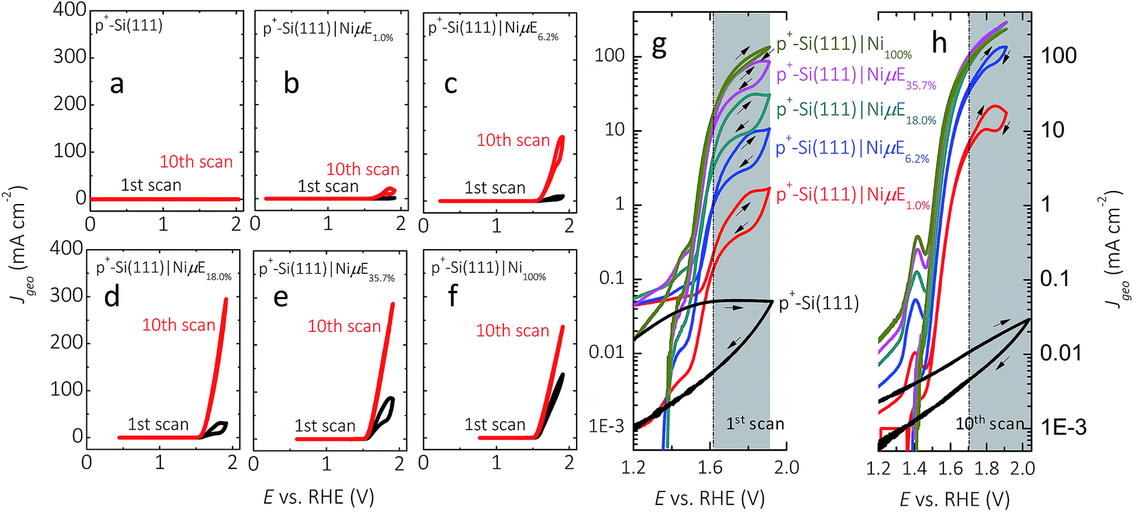 | ||
| Fig. 3 J–E behavior of p+-Si(111) electrodes patterned with Ni catalyst islands, p+-Si(111)|NiμE, in 1.0 mol L−1 KOH for the first cycle (black) and after ten cycles (red) between Eoc and +1.93 V vs. RHE. The J–E behavior of a bare, HF-treated p+-Si(111) electrode is shown in (a), and the J–E behavior of a p+-Si(111) completely covered by a Ni film is shown in (f). The Ni filling fractions were (b) 1.0%, (c) 6.2%, (d) 18.0%, and (e) 35.7%. J–E behavior in semi-log scale for the first (g) and tenth (h) potential scans in the potential window of +1.2 to +1.93 V vs. RHE. The scan rate was 40 mV s−1. | ||
| Filling fraction | E, V vs. RHE@JCat = 0.1 mA cm−2, 1st CV | E, V vs. RHE@JCat = 0.1 mA cm−2, 10th CV | J Cat, mA cm−2@1.4 V vs. RHE, 1st CV | J Cat, mA cm−2@1.4 V vs. RHE, 10th CV | Tafel slope, mV dec−1@10th CV | η (V) vs. RHE@η10 mA cm−2, 10th CV |
|---|---|---|---|---|---|---|
| 1.0% | 0.19 ± 0.01 | 1.11 ± 0.01 | 5.40 ± 0.14 | 1.02 ± 0.03 | 76 ± 5 | 0.540 ± 0.02 |
| 6.2% | 0.39 ± 0.01 | 1.29 ± 0.01 | 1.16 ± 0.03 | 0.89 ± 0.03 | 49 ± 1 | 0.407 ± 0.01 |
| 18.0% | 0.82 ± 0.01 | 1.33 ± 0.01 | 0.55 ± 0.01 | 0.64 ± 0.01 | 43 ± 4 | 0.323 ± 0.01 |
| 35.7% | 1.14 ± 0.01 | 1.34 ± 0.01 | 0.32 ± 0.01 | 0.57 ± 0.01 | 41 ± 3 | 0.354 ± 0.01 |
| 100% | 1.39 ± 0.01 | 1.39 ± 0.01 | 0.10 ± 0.01 | 0.27 ± 0.01 | 43 ± 3 | 0.344 ± 0.01 |
Fig. S5† shows the potential profiles of p+-Si(111)|NiμEs at different filling fractions operating at J = 10 mA cm−2. The stability of p+-Si(111)|NiμE with low filling fractions (1.0% and 6.2%) was a function of J. Fig. S6† shows the potential profile without resistance correction for p+-Si(111)|NiμEs at different filling fractions, operating in 1.0 mol L−1 KOH at J = 30 mA cm−2 instead of J = 10 mA cm−2. At the higher current density, p+-Si(111)|NiμE1.0% failed within 1 h operation, and substantial changes in the morphology of the Ni catalyst islands were evident after failure (Fig. S7†). Although J was fixed at 10 mA cm−2, the actual polarization of the Ni islands was a function of the fractional surface coverage of Ni, as is evident by comparing Fig. 3 and S4,† and as summarized in Table 1.
Faradaic efficiency for O2(g) evolution
Fig. 4 compares the measured volume of O2 collected from p+-Si(111)|NiμEs operated galvanostatically at J = 10 mA cm−2 to the volume of O2 that would be produced if 100% of the current passed led to evolved O2. For each of the Ni filling fractions, electrodes exhibited nearly 100% faradaic efficiency for evolution of O2. The potential needed to maintain J = 10 mA cm−2, which included the entire exposed surface containing Si and Ni, remained unchanged during the 24 h test period for samples with a Ni filling fraction >1.0%, while samples with a Ni filling fraction of 1.0% showed a slow increase followed by a large increase in overpotential.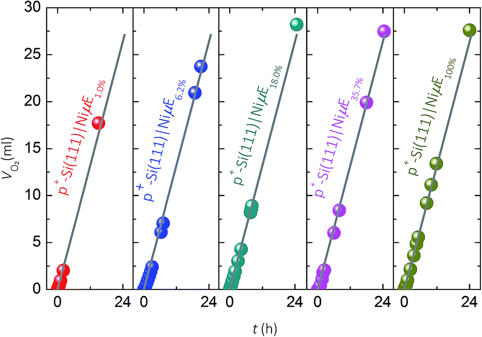 | ||
| Fig. 4 Volume of O2 measured (solid dots) as a function of time for p+-Si(111)|NiμE samples of varied Ni filling fractions in 1.0 mol L−1 KOH and at a constant J of 10 mA cm−2. Solid lines represent the calculated volume of O2 that would be generated at 100% current efficiency. p+-Si(111)|NiμE electrodes: 1.0% (red), 6.2% (blue), 18.0% (green), 35.7% (pink) and 100% (brown). | ||
During the first scan (Fig. S4a†), as the island filling fraction increased, the potential required to obtain a Jcat of 0.1 mA cm−2 increased (second column in Table 1) and the current density in the potential window of 0.2–1.2 V vs. RHE decreased. After 10 cycles of CV scans (Fig. S4b†), the potential (E) needed to achieve 0.1 mA cm−2 shifted to higher values (third column in Table 1) approaching that of the p+-Si(111)|Ni100% (e.g., 1.39 V vs. RHE). For example, E vs. RHE at Jcat = 0.1 mA cm−2 increased from 0.11 to 1.11 V, from 0.39 to 1.29, from 0.82 to 1.33, and from 1.14 to 1.34 on p+-Si samples with filling fractions of 1%, 6.2%, 18.0% and 35.7%, respectively. Furthermore, after CV scans, the value of Jcat at 1.4 V vs. RHE decreased for samples with low filling fraction (1%, 6.2% and 18.0%) and increased for samples with high filling fractions, as shown in the fourth and fifth columns of Table 1. These observations can be explained by simultaneous suppression of Si oxidation reactions on samples with large island coverages after initial anodic surface oxidation, and activation of the Ni catalyst (i.e., increased Ni redox peak at ∼1.41 V vs. RHE). Moreover, minimization of concentration-overpotential losses from radial diffusion could contribute to the improved performance of p+-Si(111)|NiμE18.0% and p+-Si(111)|NiμE35.7% at higher current densities (Jcat > 100 mA cm−2), relative to the behavior of p+-Si(111)|Ni100% electrodes.
The overpotential at a given geometric current density (10 mA cm−2) saturated after 18% filling fraction (Fig. 3h), approaching the activity typically obtained from Ni-containing catalysts in KOH solution (∼330 mV) without intentional introduction of activation species. However, as indicated by the error bar (last column in Table 1), the observed overpotentials of samples with island filling fractions above 18% should be considered mutually indistinguishable based on the available data.
Spatial dependence of O2 production
Scanning electrochemical microscopy (SECM) was used to investigate the extent to which the OER was localized to the Ni islands in 0.88 mol L−1 KOH. As shown schematically in Fig. 5a, the SECM tip current was due to reduction of O2, with the magnitude of the current proportional to the local O2 concentrations. Differences in local O2 concentration are due to different oxidation rates of OH− to O2 at different areas of the sample surface. Images were obtained after at least ten potential cycles between Eoc and + 1.95 V vs. RHE. Bare p+-Si(111) exhibited little oxygen evolution (Fig. 5b) whereas the Ni areas of p+-Si(111)|NiμE1.0% were substantially more active (∼100 nA) than the surrounding Si substrate (10 nA) (Fig. 5c and d). SECM scans of the substrate with the potential held at +1.85 V or +1.95 V vs. RHE indicated that the OER activity increased with applied potential. Relative to bare Si, the Ni-free areas on the patterned surface appeared to be more active for the OER, as evidenced by the 100-fold smaller tip current at the unmodified surface. This difference is likely due to lateral diffusion of O2 from areas above active Ni islands. Long-term SECM measurements (e.g., imaging the substrate before and after 10 CVs), were not reproducible, likely due to tip fouling. The contrast between the Ni and Si areas increased after polishing and repositioning the tip at the same sample (Fig. S8†). | ||
| Fig. 5 (a) Diagram of scanning electrochemical microscopy (SECM) of p+-Si(111)|NiμE1.0% in 0.88 mol L−1 KOH. The Pt tip (10 μm diameter) potential was +0.45 V vs. RHE while the potential of the substrate, Es, was varied. (b) Image of bare p+-Si(111) at Es = +1.95 V vs. RHE. Inset shows a narrower current scale for comparison. (c, d) Images of p+- Si(111)|NiμE1.0% at Es = +1.85 V and +1.95 V vs. RHE, respectively. The tip-substrate separation was 6 μm and the scan rate was 100 μm s−1. The SECM probe (10 μm) limits the spatial resolution of this technique, and the lack of high spatial resolution was the primary reason that SECM was only used to study samples with larger islands (10 μm) and smaller filling fractions (1%). | ||
X-ray photoelectron spectroscopy measurements of surface condition
Two p+-Si(111)|NiμE35.7% samples were examined by X-ray photoelectron spectroscopy (XPS) before and after fifty potential cycles in 0.88 mol L−1 KOH (Fig. 6). The details of the analysis are presented in the ESI.† For as-prepared specimens, the Ni islands were covered with a ∼0.8 nm thick NiO film that was terminated by a Ni(OH)2 layer (Fig. 6a), and Si was covered with a ∼0.4 nm equivalent thickness SiOx layer (Fig. 6b). Cycling resulted in further oxidization of the Ni/NiO/Ni(OH)2 islands to form a thicker Ni(OH)2/NiOOH overlayer (Fig. 6c), as expected. Likewise, anodic oxidation of Si in the surrounding field resulted in thickening of the SiOx overlayer to an equivalent thickness of ∼0.6 nm, with a much larger contribution from sub-stoichiometric species evident in the low binding-energy Si 2p XPS peak (Fig. 6d).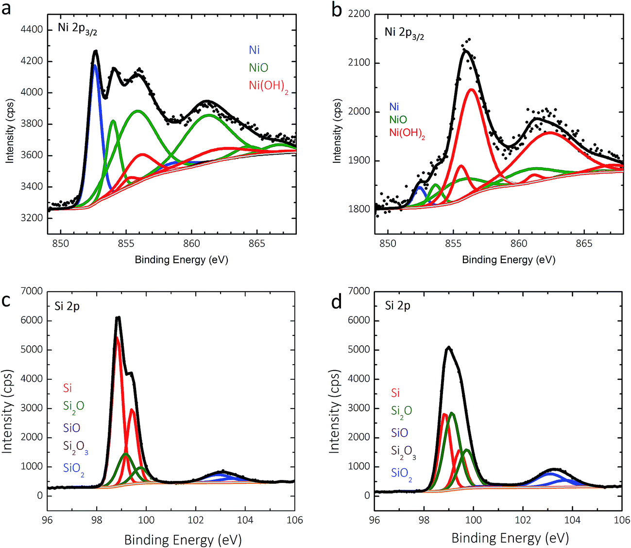 | ||
| Fig. 6 X-ray photoelectron spectra in the Ni 2p and Si 2p regions for p+-Si(111)|NiμE35.7% before (a and b) and after 50 potential cycles (c and d) at 40 mV s−1 between +0.60 V and +2.15 V vs. RHE in 0.88 mol L−1 KOH. | ||
Failure of photoactive n- and np+-Si(111)|NiμE samples
Fig. 7a shows the representative J–E behavior of a np+-Si(111)|NiμE18.0% photoelectrode after 240 and 265 h in 1.0 mol L−1 KOH. The Eoc continuously shifted positively, from −110 to −70 to −30 mV vs. E0′(O2/H2O), while the current density at E0′(O2/H2O) decreased from 12.7 to 4.6 to 0.9 mA cm−2, after 240 h and 265 h of operation at +1.73 V. vs. RHE, respectively. A stable chronoamperometric response was observed during the first 240 h of operation (Fig. 2c), but the light-limited photocurrent density at potentials more positive than ∼1.4 V vs. RHE decreased to values below 12.5 mA cm−2 after 265 h of operation. Morphological studies using SEM (Fig. 7b) revealed a substantial volume expansion around the edges of the catalyst islands, where the current and electric field were concentrated. Isotropic etching of both the p+-Si emitter and the n-Si substrate underneath and surrounding the catalyst islands was also observed, and is likely the predominant factor that led to the loss of the catalyst islands from the Si substrate.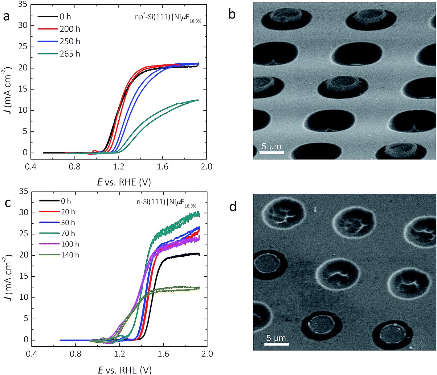 | ||
| Fig. 7 Extended stability studies of np+- and n-Si(111)|NiμE samples. (a) J–E behavior of a np+-Si(111)|NiμE18.0% photoelectrode collected periodically during the chronoamperometric stability test at 1.73 V vs. RHE. (b) SEM image of np+-Si(111)|NiμE18.0% after a 265 h stability test. (c) J–E behavior of the n-Si(111)|NiμE18.0% photoelectrode collected periodically during the chronoamperometric stability test at 1.93 V vs. RHE. (d) SEM image of n-Si(111)|NiμE18.0% after a 140 h stability test. The voltammetric scan rate was 40 mV s−1 for (a) and (c). | ||
Fig. 7c shows the J–E behavior of a photoactive n-Si(111)|NiμE18.0% sample (without a np+ junction) during a 140 h stability test. The light-limited photocurrent density and the photovoltage both increased during the first 100 h of operation. The Eoc shifted from +190 to +30 mV and to −100 mV vs. E0′(O2/H2O), the current density at E0′(O2/H2O) increased from 0.0 to 0.6 and to 3.6 mA cm−2 after 70 h and 100 h, respectively. The ηIRC increased from 0.0 to 0.1% after 100 h of operation. The light-limited photocurrent density at +1.93 V vs. RHE slowly increased from 20.0 to 29.8 mA cm−2 during the first 70 h of operation, but decreased after 70 h, and by 140 h the light-limited photocurrent density decreased to <12.5 mA cm−2. The different trends in Eoc and light-limited photocurrent densities versus time – decreasing for the np+-Si(111)|NiμE18.0% sample but increasing for the n-Si(111)|NiμE18.0% sample during the first 100 h – indicates damage to the emitter layer of the np+-Si(111)| NiμE18.0% device. Similar to the np+-Si(111)|NiμE18.0% sample, SEM indicated etching of Si and loss of Ni catalyst islands (Fig. 7d) after 140 h of operation. A comparison of images of as-prepared samples (Fig. 1) with the images in Fig. 7 provides evidence of undercutting of the Ni islands. Additional cross-sectional images of the samples could provide valuable additional details on the progression of the undercutting process.
Stability of p+-Si(100)|NiμEs under open-circuit conditions
The stability of the Si surface under open-circuit conditions was investigated for Ni catalyst islands on Si(100) surfaces. The dissolution rate of Si(100) in alkaline media is substantially larger than that of Si(111).47 The dissolution rate of Si is also sensitive to the electrode potential, and exhibits a maximum near open circuit.Fig. 8 shows the electrochemical stability as a function of time at open circuit for a p+-Si(100)|NiμE18% sample. The p+-Si(100)|NiμE18.0% was immersed for 70 h in 1.0 mol L−1 KOH in the dark, and 10 potential cycles between Eoc and +1.93 V vs. RHE were obtained every 14 h. The p+-Si(100)|NiμE18.0% was electrochemically stable for 42 h at open circuit (three 14 h periods), and the catalytically active surface area, as reflected by the charge density of the Ni oxide reduction peak (inset of Fig. 8), did not change over this time period. However, the J–E behavior of the electrode deteriorated after 56 h at open circuit, and the overpotential required to drive the OER at J = 10 mA cm−2 increased from 340 mV to 440 mV and further to >+1.0 V after 70 h, accompanied by a substantial reduction in the active surface area of the electrode.
 | ||
| Fig. 8 Electrochemical stability of p+-Si(100)|NiμE18% at open circuit in 1.0 mol L−1 KOH. J–E characteristics were measured before (0 h) and after each 14 h period at open circuit, and the potential axis is the overpotential referenced to E0′(O2/H2O). The inset shows the Ni redox region of the J–E data, and the size of the peaks in this region reflects the catalytically active surface area. | ||
Effect of Ni film thickness on electrocatalytic activity
Fig. S9† shows the voltammetry of uniform Ni films with varying thickness on p+-Si(111) in a potassium ferricyanide/ferrocyanide, Fe(CN)63−/4−, solution, and the electrocatalytic activity of similar films after activation in 1.0 mol L−1 KOH. For an ultrathin Ni film (1 nm, black curves in Fig. S9†), the charge-transfer kinetics were limited, as evidenced by the near-zero slope of the J–E behavior across E = 0, the decreased current at a fixed potential relative to samples with thicker Ni films, and by an overpotential of >600 mV at 10 mA cm−2. In contrast, for Ni films with thickness >2 nm, the J–E behavior during the CV measurements in both solutions was independent of the thickness of the Ni.Discussion
Effects of patterned catalysts on resistance loss, catalytic activity, optical absorption, and interfacial energetics
Similar to a metal grid on the front surface of a photovoltaic device, the geometric design of patterned catalysts on photoanodes needs to be optimized to both maximize light absorption by the underlying semiconductor and minimize majority-carrier recombination losses associated with the semiconductor–catalyst junction. For example, a low filling fraction of catalyst islands reduces shadowing effects while maximizing the solution/semiconductor junction area for charge separation.45,48–50 Moreover, at a constant filling fraction, a smaller diameter and spacing of the catalyst islands minimizes the resistance losses and thus improves the charge-collection efficiency. However, after activation, the current is concentrated at the catalyst islands, where the current densities normalized to the catalyst-island coverage, Jcat, are 3 to 100 times larger than the geometric current densities, J. The overpotential and electrochemical stability at high Jcat values of 30–1000 mA cm−2, based on an integrated device operating at 10% STH (solar-to-hydrogen) conversion efficiency, are thus important parameters.45 The thickness of the metal catalyst also affects the conductivity and the electrocatalytic activity of photoanodes,51 because the catalyst layer must be thick enough to be nonporous during operation and prevent corrosion of the semiconductor underneath the catalyst islands. Of the samples examined in this work, Ni disks with 10 μm diameter and a filling fraction of 18.0% generated the highest electrocatalytic activity after 10 potential cycles (Fig. 3), and Ni films thicker than 2 nm were able to provide stable electrochemical response for at least 10 cycles of CV measurement (Fig. S9†).Charge transfer at the semiconductor/metal-catalyst interface is another important factor in device design. Photovoltages of >550 mV have been reported for n-Si|Ni surfaces formed by evaporation of Ni onto a Si electrode that was covered with a native oxide.16 However, Si surfaces with little to no native oxide will have a high density of surface states and metal-induced gap states, both of which can pin the surface Fermi level, generally resulting in low barrier heights.52 For such a situation, the recombination current due to majority-carrier thermionic emission will be large, even for 10% coverage of metal on the electrode surface. A metal/semiconductor “nanoemitter” strategy, i.e., formation of an underlying buried homogeneous junction or passivation/tunneling junction on a buried np+ interface, results in a higher barrier height and thus lower majority-carrier recombination-emission currents that lead to an increased photovoltage of the device.53–56 A comparison of Fig. 7a and c demonstrates that the applied potential required to generate 10 mA cm−2 was 300 mV less for np+-Si(111)|NiμE photoanodes than for n-Si(111)|NiμE photoanodes. Alternatively, using a nanoscale array of catalyst islands deposited directly onto n-Si without a p+-Si emitter layer, instead of the microscale catalyst islands deposited onto np+-Si(111) used herein, could allow exploitation of pinch-off effects resulting from mixed barrier heights near the emitter/catalyst islands that could allow high photovoltages from island-covered photoelectrodes without buried junction emitters.27,57 This strategy could be especially useful for nearly transparent metal films that enable beneficial use of high filling fractions of active catalysts on the photoelectrode surface.58 In addition, if a silicide is formed at the Si/Ni interface, such as after annealing, an ohmic contact to the emitter region of the Si photoanode is produced, lowering the barrier height at the Si/Ni contact. Electrochemical impedance spectroscopy could provide additional insight into charge transfer at the semiconductor/catalyst interface; however, the usefulness of such analyses would depend on the future development of sufficiently accurate models of the mixed interfaces and coupled reactions in these devices.
Degradation pathways and failure mechanisms
Passivating thin films and patterned catalysts have been used to improve the performance and stability for a variety of photoelectrodes. While patterned arrays of metal electrocatalysts on oxide-passivated Si photoelectrodes are stable in acid electrolytes, in alkaline media Si undergoes anisotropic etching and micromachining. Both n- and p-type Si have been well studied under open-circuit conditions in concentrated KOH. At open circuit, both n-Si and p-Si become covered with surface hydrides and actively dissolve, with Si(100) surfaces etching more rapidly than Si(111) surfaces, undercutting any masking material and leaving pyramidal etch pits on the surface.59 The rapid decrease in catalytic activity of p+-Si(100)|NiμE electrodes observed herein (Fig. 8) is consistent with the decrease in catalytically active surface area due to the anisotropic dissolution of Si(100) in 1 mol L−1 KOH(aq.) followed by facile undercutting of the catalyst islands (Fig. 9a). Therefore, prevention of failures in Si electrodes left at open circuit while in contact with a strongly alkaline electrolyte may require barrier layers that are impenetrable to the electrolyte.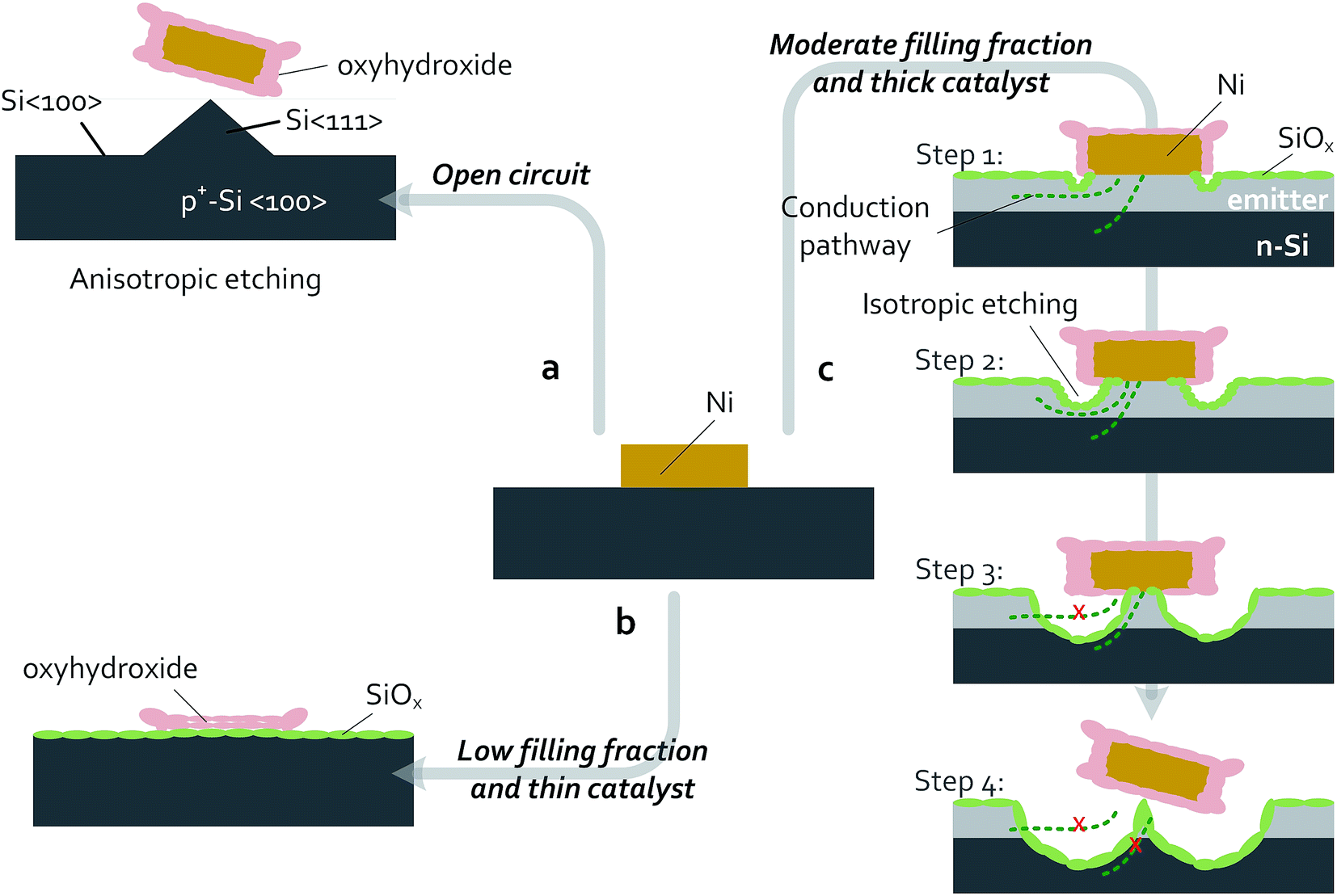 | ||
| Fig. 9 Schematic of failure-process pathways for Si|NiμEs during OER in 1 mol L−1 KOH. Processes observed using non-photoactive p+-Si|NiμE devices are shown in (a) and (b), while processes observed using photoactive np+-Si/NiμE devices or n-Si|NiμE devices are shown in (c). Green indicates a SiOx layer, light gray indicates a p+-Si emitter layer, orange is metallic Ni, and pink is the Ni oxyhydroxide/hydroxide layer. Dimensions are not to scale. (a) Anisotropic etching of Si(100), resulting in removal of the patterned NiμEs occurs for devices left at open circuit. (b) For devices with low Ni filling fractions (1.0 and 6.2%) or thin catalyst layers, during OER, the Ni layer is fully converted to a porous, highly active oxyhydroxide catalyst that results in failure of the devices due to complete passivation of Si surfaces, including the Si surface beneath the catalyst islands. The full passivation of the Si surface by an insulating layer of SiOx ultimately blocks current flow. (c) Passivation of Si surfaces by a SiOx layer occurs for samples with moderate Ni filling fractions (18.0 and 35.7%) under OER conditions. Isotropic etching of the passivating SiOx occurs preferentially near the Ni islands and competes kinetically with the OER. For samples with a p+-Si emitter layer, etching of the emitter damages the buried junction and limits conduction of charge carriers to the catalyst island. Ultimately, isotropic etching near the Ni islands under OER conditions undercuts and removes the catalyst islands. | ||
At more positive potentials, etching of Si can be minimized by conversion of the active Si–H surface into SiOx.60 During operation of p+-Si(111)|NiμEs in the OER regime, the SiOx layer effectively passivates the Si surface (Fig. 3 and 6), the catalytic Ni islands become activated and convert essentially 100% of the available current to O2(g). Combining the behavior of the patterned p+-Si(111)|Ni surface with a buried homogenous junction, e.g., np+-Si(111)|Ni, enabled light-limited photoelectrochemical OER performance for at least 240 h of continuous operation (Fig. 2). The failure of the Si(111) electrodes patterned with low Ni filling fractions (1.0% and 6.2%) can be ascribed to morphological changes to the NiμEs. Under OER conditions at small filling fractions and thus large JCat (100–1000 mA cm−2), the metallic Ni catalyst islands with a thin (15 nm) Ni layer can be fully converted to active oxyhydroxides capable of carrying large catalytic current densities (16–100 times larger than the geometric current density) compared to thicker films that have lower Ni surface-area-to-volume ratios. The conversion of the Ni layer to a porous Ni oxyhydroxide that is permeable to the electrolyte solution, possibly combined with Fe intercalation, results in a substantial volumetric expansion and consequent change in morphology (Fig. 9b and S7†). The underlying Si has a higher tendency to be converted into Si oxide through the ion-permeable layer, resulting in an increase in the resistance loss at the interface and eventually producing a blockage of charge conduction between the Si and the catalyst-coated regions of the device.
Ellipsometric monitoring of oxide dissolution under open-circuit conditions has indicated dissolution rates of 0.06 nm min−1, 0.01 nm min−1, and 0.005 nm min−1 for the oxide formed electrochemically on p-Si(111), thermal silicon oxide, and bulk silica, respectively.61 Therefore, at a given oxidation potential, a steady-state film thickness can be established based on the dynamic balance between formation and dissolution of the silicon oxide layer. If the oxide-dissolution rate is independent of applied potential, these values can be used to estimate the failure time of the Si|Ni electrodes based either on undercutting of the metal islands by slow SiOx dissolution and/or etching into the np+ junction. At catalyst filling fractions ≥18.0%, the dynamic balance between the formation and etching of a passivating oxide layer did not result in degraded electrical stability within 24 h of measurement using non-photoactive electrodes, and consequently the potentials needed to drive a geometric current density at both 10 mA cm−2 and 30 mA cm−2 remained stable (Fig. S5 and S6†).
SECM measurements (Fig. 5) demonstrated that the Ni islands on p+-Si(111)|NiμEs were more reactive for water oxidation than the surrounding p+-Si(111) substrate. Faradaic efficiency measurements confirmed that ∼100% of the current for oxygen-evolution reactions flowed through the Ni catalyst islands. However, after these experiments, physical damage was observed to the substrates, as shown in the SEM images in Fig. 7b and d for np+- and n-Si (111). Therefore, the anodic formation, and isotropic etching, of SiOx on catalyst-island-patterned Si surfaces are likely inhomogeneous under OER conditions. These observations are consistent with a localized process that is initiated at the edges of activated catalyst islands and/or at defects within the catalyst film where the electric field is primarily concentrated (step 1 in Fig. 9c). Further experiments with varied catalyst fill fractions and varied shapes of catalyst islands, or both, could provide valuable insight into the importance of the current-density profile to localization of isotropic etching of SiOx under OER conditions.
The improvements in photocurrent densities and photovoltages observed during the stability test of n-Si(111)|NiμE photoanodes with moderate filling fractions (18%) are consistent with growth of an interfacial oxide under the catalyst islands (from the edges or defects). The anodic interfacial oxide formed minimizes the deleterious effect of low-barrier-height regions caused by surface states or metal silicides.27 In addition, oxides formed at unprotected areas can also passivate bare Si surfaces and improve the efficiency of charge collection at the Ni islands.
However, etching of the emitter layer on np+-Si(111)|NiμE photoanodes below the catalyst islands degraded the barrier height and increased the resistance by producing a thinner emitter during lateral collection of carriers (step 2 and 3 in Fig. 9c). Etching through the emitter layer and eventual detachment of the catalyst islands (step 4 in Fig. 9c) destroyed the homogeneous junction, reducing the OER reactivity, resulting in a positively shifted onset voltage of the photocurrent, and reduced the light-limited photocurrent density, as shown in the J–E behavior of Fig. 7a.
Current branching occurs when both active catalysts and corrosive solution are present, where the current is distributed between that for formation of a silicon oxide, JSOR, and the OER current, JOER. Assuming that the dynamic process underneath the island is not limited by mass transport, and that the oxidation of Si and dissolution of SiO2 are 4-electron processes, an upper limit for the current branching ratio, JSOR/JOER, of 5.6 × 10⁻⁴ can be calculated based on the total charge needed to completely undercut the catalyst islands and the total charge passed during the stability tests performed in this work (see ESI for details†). The lower limit of the operational lifetime of Si photoanodes based on such a catalyst-island design is therefore a function of the size of the island, the filling fraction, the catalytic activity of the islands, and the geometric photocurrent density. The current branching is a competitive process that depends in part on the catalytic overpotential for the OER, i.e. increasing the activity of the OER catalyst will decrease JSOR/JOER. Thus, methods of increasing the activity of the Ni catalyst, such as intentional incorporation of Fe,62 may provide increased lifetimes of Si photoanodes patterned with catalysts. The size of the catalyst islands and the catalyst-filling fractions are additional interesting parameters for further examination of the catalyst-island design. Although an electrode design that uses smaller islands improves the charge-collection efficiency and reduces the resistance losses, failure of such electrodes likely will occur more rapidly than for designs with larger islands, because the smaller area of the island would mean that less material would need be undercut before the island fails, assuming that undercutting of the catalysts is the predominant failure mechanism. Although for the same filling fraction of Ni, failure would occur more rapidly for smaller islands, reducing the island size should also reduce the current densities near small islands relative to current densities near larger islands, and thus may reduce the rate of preferential etching near the edges of catalyst islands.
Applicability of observed degradation pathways to other systems
n-Si(100) photoanodes coated with randomly dispersed, 60 nm diameter electrodeposited Ni nanoparticles have exhibited photovoltages of >360 mV and light-limited photocurrent densities of >20 mA cm−2 for water oxidation under 100 mW cm−2 of simulated Air Mass 1.5G illumination in contact with 1 M NaOH(aq.).32 The catalytic performance was ascribed to generation of an effective, inhomogeneous metal–insulator–semiconductor Ni–SiOx–Si interface, with thicker catalytic layers yielding lower photocurrent densities and photovoltages but better physical protection against growth of silicon oxide and etching of the Si(100) surface in contact with strong base. Core–shell Ni/Ni(OH)2 nanoparticles electrodeposited onto n-Si have yielded photovoltages of ∼400 mV for up to 300 h in contact with aqueous borate (pH 9) buffer.33Catalytic, transparent, protective coatings constitute an alternative to catalyst islands for obtaining stable, high-performance photoanodes using semiconductors that are unstable under oxygen-evolution conditions.23–25,28,29 Ultrathin metallic or metal oxide films are non-uniform; hence, direct contact between the substrate and electrolyte can occur near pinholes or other defects in such films. Therefore, to obtain extended photoanode stability, both the patterned-catalyst and the protective thin-film approaches require minimization of the corrosion of the semiconducting substrate by formation of a relatively insoluble surface layer. The density and size of pinholes in these protective films are difficult to control experimentally, so patterned-catalyst devices offer an opportunity to explore experimentally the failure mechanisms that may govern the long-term stability of Si photoanodes protected by other transparent catalytic films. Based on the present study, we speculate that failures of Si photoanodes protected by sputtered NiOx films or any other ultrathin catalytic films, e.g., metallic Ni or other catalytic oxides, under OER conditions will result from the gradual loss of substrate at the defects, especially near active catalysts where the current is primarily concentrated. We additionally speculate that undercutting of ultrathin catalytic films or sputtered NiOx films will occur for such devices left at open circuit while in contact with strongly alkaline aqueous electrolytes.
In the absence of validated accelerated stability-testing protocols for integrated devices, determination of primary failure mechanisms in these devices will benefit from in situ monitoring of the catalytic activity,27 charge-transfer resistance, interfacial energetics (especially for devices without homogeneous buried junctions),27 external quantum efficiency (likely affected by changes in the complex refractive index of the protective coating),51 as well as by in-depth structural characterization (e.g., SEM and HR-TEM) of devices after electrochemical stability testing, that involve the operation of individual devices for hundreds of hours or more prior to characterization. Such structural characterization should focus on the time-dependent change in thickness of the insulating SiOx layer between the photoactive substrate and the catalyst islands (or sputtered coating), the spatial distribution of SiOx growth at regions not covered by catalyst islands, and on monitoring the growth rate of etch pits that undercut catalyst islands or damage buried junctions. Although failure by undercut etching may be inherent to all anodes that rely on protection by a SiOx layer in contact with a strongly alkaline aqueous electrolyte, increasing the thickness of the SiOx and catalyst layers, along with increased filling fraction of catalyst on the surface may result in devices with substantially increased lifetimes relative to those examined herein.
Conclusions
An oxygen-evolving photoanode that was stable for 240 h in 1.0 mol L−1 KOH was constructed using patterned Ni catalyst islands on Si, without additional prefabricated protection layers. Exposed Si areas not covered by catalyst islands passivated under light during operation by formation of a relatively insoluble, insulating layer of SiOx. After passivation of the exposed Si areas, the oxidation current was channeled through the activated Ni catalyst islands. However, the passivating SiOx coating dissolves in KOH, resulting in Si corrosion and SiOx dissolution especially in the dark. This process requires engineering solutions to protect Si photoanodes used for sunlight-driven oxygen evolution when the sun goes down or when cloud cover is substantial. The dynamic processes of SiOx formation and etching affect both the electrical stability of the electrochemical and photovoltaic components, as well as the optoelectronic stability of the photovoltaic component. Localized undercutting of catalyst islands and damage to the emitter profile correlated with the current distribution on sample surfaces, suggesting substantial current branching at the location where the active catalysts and the corrosive solution are both present. This work provides evidence of one likely failure mechanism for Si photoanodes protected by transparent catalytic films, specifically, undercutting and removal of the catalysts at defects in protective coatings that can arise during fabrication, deployment and operation. Future experimental efforts to elucidate the mechanism underlying the apparent acceleration of etch rates near catalyst islands could provide valuable insights into the competitive processes of passivation and etching, and such results could be combined with three-dimensional multi-physics modeling to determine the catalyst filling fractions and island diameters that provide optimal efficiency and stability for the catalyst-island design.Author contributions
K. S. and N. S. L designed research; K. S., N. R., J. J., H. T., W. G. H., J. J., I. A. M., and T. P. M. performed experiments; K. S., N. R., J. J., H. T., K. M. P., T. P. M., B. S. B., and N. S. L. analyzed data; and K. S., N. R., K. M. P., T. P. M., B. S. B., and N. S. L. wrote the paper.Conflicts of interest
There are no conflicts to declare.Acknowledgements
This material is based upon work performed by the Joint Center for Artificial Photosynthesis, a DOE Energy Innovation Hub, supported through the Office of Science of the U.S. Department of Energy under award no. DE-SC0004993. UV-vis spectroscopy was performed at the Molecular Materials Research Center (MMRC) in the Beckman Institute at the California Institute of Technology. This work was also supported by the Gordon and Betty Moore Foundation under award no. GBMF1225. We thank A. Carim, M. Shaner, F. Saadi, J. Velazquez, and C. Xiang from Caltech for stimulating discussions. We also thank K. Walczak (Lawrence Berkeley National Laboratory) for preparation of the ion-implanted Si n+np+ substrates. The NIST work was supported by the American Recovery and Reinvestment funds. N. L. R. acknowledges the National Institute of Standards and Technology-National Research Council research associateship program for a postdoctoral fellowship.References
- M. Pourbaix, Atlas of Electrochemical Equilibria in Aqueous Solutions, National Association of Corrosion Engineers, Houston, Texas, 1974 Search PubMed.
- S. Chen and L.-W. Wang, Chem. Mater., 2012, 24, 3659–3666 CrossRef CAS.
- A. J. Bard and M. S. Wrighton, J. Electrochem. Soc., 1977, 124, 1706–1710 CrossRef CAS.
- J. R. McKone, N. S. Lewis and H. B. Gray, Chem. Mater., 2014, 26, 407–414 CrossRef CAS.
- Y. W. Chen, J. D. Prange, S. Dühnen, Y. Park, M. Gunji, C. E. D. Chidsey and P. C. McIntyre, Nat. Mater., 2011, 10, 539–544 CrossRef CAS PubMed.
- S. Hu, M. R. Shaner, J. A. Beardslee, M. Lichterman, B. S. Brunschwig and N. S. Lewis, Science, 2014, 344, 1005–1009 CrossRef CAS PubMed.
- M. Shaner, S. Hu, K. Sun and N. S. Lewis, Energy Environ. Sci., 2015, 8, 203–207 CAS.
- N. C. Strandwitz, D. J. Comstock, R. L. Grimm, A. C. Nichols-Nielander, J. Elam and N. S. Lewis, J. Phys. Chem. C, 2013, 117, 4931–4936 CAS.
- K. Jun, Y. S. Lee, T. Buonassisi and J. M. Jacobson, Angew. Chem., Int. Ed., 2012, 51, 423–427 CrossRef CAS PubMed.
- K. Sun, N. Park, Z. Sun, J. Zhou, J. Wang, X. Pang, S. Shen, S. Y. Noh, Y. Jing, S. Jin, P. Yu and D. Wang, Energy Environ. Sci., 2012, 5, 7872–7877 CAS.
- K. Sun, X. Pang, S. Shen, X. Qian, J. S. Cheung and D. Wang, Nano Lett., 2013, 5, 2064–2072 CrossRef PubMed.
- R. Liu, Z. Zheng, J. Spurgeon and X. Yang, Energy Environ. Sci., 2014, 7, 2504–2517 CAS.
- J. Yang, K. Walczak, E. Anzenberg, F. M. Toma, G. Yuan, J. Beeman, A. Schwartzberg, Y. Lin, M. Hettick, A. Javey, J. W. Ager, J. Yano, H. Frei and I. D. Sharp, J. Am. Chem. Soc., 2014, 136, 6191–6194 CrossRef CAS PubMed.
- J. C. Hill, A. T. Landers and J. A. Switzer, Nat. Mater., 2015, 14, 1150–1155 CrossRef CAS PubMed.
- J. Yang, J. K. Cooper, F. M. Toma, K. A. Walczak, M. Favaro, J. W. Beeman, L. H. Hess, C. Wang, C. Zhu, S. Gul, J. Yano, C. Kisielowski, A. Schwartzberg and I. D. Sharp, Nat. Mater., 2016, 16, 335–341 CrossRef PubMed.
- M. J. Kenney, M. Gong, Y. Li, J. Z. Wu, J. Feng, M. Lanza and H. Dai, Science, 2013, 342, 836–840 CrossRef CAS PubMed.
- K. Sun, S. Shen, J. S. Cheung, X. Pang, N. Park, J. Zhou, Y. Hu, Z. Sun, S. Y. Noh, C. T. Riley, P. K. L. Yu, S. Jin and D. Wang, Phys. Chem. Chem. Phys., 2014, 16, 4612–4625 RSC.
- X. Yu, P. Yang, S. Chen, M. Zhang and G. Shi, Adv. Energy Mater., 2016, 7, 1601805 CrossRef.
- K. Yoon, J.-H. Lee, J. Kang, J. Kang, M. J. Moody, M. C. Hersam and L. J. Lauhon, Nano Lett., 2016, 16, 7370–7375 CrossRef CAS PubMed.
- X. Zhou, R. Liu, K. Sun, K. M. Papadantonakis, B. S. Brunschwig and N. Lewis, Energy Environ. Sci., 2016, 9, 892–897 CAS.
- A. Azarpira, T. Schedel-Niedrig, H. J. Lewerenz and M. Lublow, Adv. Energy Mater., 2016, 6, 1502314 CrossRef.
- Y. Yu, Z. Zhang, X. Yin, A. Kvit, Q. Liao, Z. Kang, X. Yan, Y. Zhang and X. Wang, Nat. Energy, 2017, 2, 17045 CrossRef CAS.
- K. Sun, M. T. McDowell, A. C. Nielander, S. Hu, M. R. Shaner, F. Yang, B. S. Brunschwig and N. S. Lewis, J. Phys. Chem. Lett., 2015, 6, 592–598 CrossRef CAS PubMed.
- X. Zhou, R. Liu, K. Sun, D. Friedrich, M. T. McDowell, F. Yang, S. T. Omelchenko, F. H. Saadi, A. C. Nielander, S. Yalamanchili, K. M. Papadantonakis, B. S. Brunschwig and N. S. Lewis, Energy Environ. Sci., 2015, 8, 2644–2649 CAS.
- K. Sun, F. H. Saadi, M. F. Lichterman, W. G. Hale, H.-P. Wang, X. Zhou, N. T. Plymale, S. T. Omelchenko, J.-H. He, K. M. Papadantonakis, B. S. Brunschwig and N. S. Lewis, Proc. Natl. Acad. Sci. U. S. A., 2015, 112, 3612–3617 CAS.
- K. Sun, R. Liu, Y. Chen, E. Verlage, N. S. Lewis and C. Xiang, Adv. Energy Mater., 2016, 6, 1600379 CrossRef.
- F. A. L. Laskowski, M. R. Nellist, R. Venkatkarthick and S. W. Boettcher, Energy Environ. Sci., 2017, 10, 570–579 CAS.
- K. Sun, Y. Kuang, E. Verlage, B. S. Brunschwig, C. W. Tu and N. S. Lewis, Adv. Energy Mater., 2015, 5, 1402276 CrossRef.
- K. Sun, S. Shen, Y. Liang, P. E. Burrows, S. S. Mao and D. Wang, Chem. Rev., 2014, 114, 8662–8719 CrossRef CAS PubMed.
- S. Oh and J. Oh, J. Phys. Chem. C, 2016, 120, 133–141 CAS.
- L. Ji, H.-Y. Hsu, X. Li, K. Huang, Y. Zhang, J. C. Lee, A. J. Bard and E. T. Yu, Nat. Mater., 2017, 16, 127–131 CrossRef CAS PubMed.
- G. Loget, B. Fabre, S. Fryars, C. Mériadec and S. Ababou-Girard, ACS Energy Lett., 2017, 2, 569–573 CrossRef CAS.
- G. Xu, Z. Xu, Z. Shi, L. Pei, S. Yan, Z. Gu and Z. Zou, ChemSusChem, 2017, 10, 2897–2903 CrossRef CAS PubMed.
- W. S. Rasband, ImageJ, http://imagej.nih.gov/ij/ Search PubMed.
- L. Trotochaud, S. L. Young, J. K. Ranney and S. W. Boettcher, J. Am. Chem. Soc., 2014, 136, 6744–6753 CrossRef CAS PubMed.
- A. J. Bard, R. Parsons and J. Jordan, Standard Potentials in Aqueous Solution, International Union of Pure and Applied Chemistry, 1985 Search PubMed.
- J. Mayer, L. A. Giannuzzi, T. Kamino and J. Michael, MRS Bull., 2011, 32, 400–407 CrossRef.
- S. Gaudet, P. Desjardins and C. Lavoie, J. Appl. Phys., 2011, 110, 113524 CrossRef.
- R. T. Tung, J. M. Gibson and J. M. Poate, Phys. Rev. Lett., 1983, 50, 429–432 CrossRef CAS.
- R. J. Hauenstein, T. E. Schlesinger, T. C. McGill, B. D. Hunt and L. J. Schowalter, Appl. Phys. Lett., 1985, 47, 853–855 CrossRef CAS.
- M. Ospelt, J. Henz, L. Flepp and H. v. Känel, Appl. Phys. Lett., 1988, 52, 227–229 CrossRef CAS.
- N. S. Dellas, B. Z. Liu, S. M. Eichfeld, C. M. Eichfeld, T. S. Mayer and S. E. Mohney, J. Appl. Phys., 2009, 105, 094309 CrossRef.
- M. R. Shaner, K. T. Fountaine and H.-J. Lewerenz, Appl. Phys. Lett., 2013, 103, 143905 CrossRef.
- R. H. Coridan, A. C. Nielander, S. A. Francis, M. T. McDowell, V. Dix, S. M. Chatman and N. Lewis, Energy Environ. Sci., 2015, 8, 2886–2901 CAS.
- Y. Chen, K. Sun, H. Audesirk, C. Xiang and N. S. Lewis, Energy Environ. Sci., 2015, 8, 1736–1747 CAS.
- D. A. Corrigan, J. Electrochem. Soc., 1987, 134, 377 CrossRef CAS.
- P. Allongue, V. Costa-Kieling and H. Gerischer, J. Electrochem. Soc., 1993, 140, 1018–1026 CrossRef CAS.
- M. Lublow, B. Bouabadi and S. Kubala, Sol. Energy Mater. Sol. Cells, 2012, 107, 56–62 CrossRef CAS.
- A. G. Muñoz and H. J. Lewerenz, ChemPhysChem, 2010, 11, 1603–1615 CrossRef PubMed.
- T. Stempel, M. Aggour, K. Skorupska, A. Muñoz and H.-J. Lewerenz, Electrochem. Commun., 2008, 10, 1184–1186 CrossRef CAS.
- K. Sun, I. A. Moreno-Hernandez, W. C. Schmidt, X. Zhou, J. C. Crompton, R. Liu, F. H. Saadi, Y. Chen, K. M. Papadantonakis and N. S. Lewis, Energy Environ. Sci., 2017, 10, 987–1007 CAS.
- W. Mönch, J. Vac. Sci. Technol., B, 1999, 17, 1867–1876 Search PubMed.
- A. Heller, Science, 1984, 223, 1141–1148 CAS.
- J. S. Kilby, J. W. Lathrop and W. A. Porter, U.S. Pat., 4,021,323, 1977.
- D. V. Esposito, I. Levin, T. P. Moffat and A. A. Talin, Nat. Mater., 2013, 12, 562–568 CrossRef CAS PubMed.
- L. Ji, M. D. McDaniel, S. Wang, A. B. Posadas, X. Li, H. Huang, J. C. Lee, A. A. Demkov, A. J. Bard, J. G. Ekerdt and E. T. Yu, Nat. Nanotechnol., 2015, 10, 84–90 CrossRef CAS PubMed.
- R. C. Rossi and N. S. Lewis, J. Phys. Chem. B, 2001, 105, 12303–12318 CrossRef CAS.
- J. D. Porter, A. Heller and D. E. Aspnes, Nature, 1985, 313, 664–666 CrossRef CAS.
- O. J. Glembocki, R. E. Stahlbush and M. Tomkiewicz, J. Electrochem. Soc., 1985, 132, 145–151 CrossRef CAS.
- E. D. Palik and V. M. Bermudez, J. Phys. Colloq., 1983, 44, C10 CrossRef.
- E. D. Palik, J. W. Faust, H. F. Gray and R. F. Greene, J. Electrochem. Soc., 1982, 129, 2051–2059 CrossRef CAS.
- L. Trotochaud, S. L. Young, J. K. Ranney and S. W. Boettcher, J. Am. Chem. Soc., 2014, 136, 6744–6753 CrossRef CAS PubMed.
Footnote |
| † Electronic supplementary information (ESI) available. See DOI: 10.1039/c7se00583k |
| This journal is © The Royal Society of Chemistry 2018 |