
Preparation of mixed-ion and inorganic perovskite films using water and isopropanol as solvents for solar cell applications†
Kári
Sveinbjörnsson
a,
Nan Kyi
Kyi Thein
 ac,
Zahra
Saki
ad,
Sebastian
Svanström
b,
Wenxing
Yang
a,
Ute B.
Cappel
b,
Håkan
Rensmo
b,
Gerrit
Boschloo
a,
Kerttu
Aitola
a and
Erik M. J.
Johansson
*a
ac,
Zahra
Saki
ad,
Sebastian
Svanström
b,
Wenxing
Yang
a,
Ute B.
Cappel
b,
Håkan
Rensmo
b,
Gerrit
Boschloo
a,
Kerttu
Aitola
a and
Erik M. J.
Johansson
*a
aUppsala University, Department of Chemistry – Ångström Laboratory, Physical Chemistry, Box 523, 751 20 Uppsala, Sweden. E-mail: erik.johansson@kemi.uu.se
bUppsala University, Department of Physics and Astronomy, Molecular and Condensed Matter Physics, Box 516, 751 20 Uppsala, Sweden
cMandalay University, Department of Physics – Materials Science Research Laboratory, Mandalay, Myanmar
dSharif University of Technology, Physics Department, Tehran 14588, Iran
First published on 14th December 2017
Abstract
Presently, the most efficient lead halide perovskite solar cells are manufactured by using high-boiling point organic solvents to dissolve the perovskite precursor materials prior to the perovskite formation. Previously, efforts have been made to exchange the said solvents for water with some success. Herein, we build on that work to develop a procedure for synthesising perovskite absorbers using only water and isopropanol as solvents. Our technique can be utilised for fabricating many different perovskite compositions, organic and inorganic. The technique is based on the high solubility of metal nitrates, such as lead(II) nitrate and caesium(I) nitrate, in water and, respectively, their poor solubilities in isopropanol. The inclusion of CsNO3 to Pb(NO3)2 films does not result in a phase separation of the perovskite material as one would expect when using lead(II) halide precursor films. Using the perovskite composition Cs0.1FA0.9Pb(I0.83Br0.17)3 we were able to reach an average solar cell power conversion efficiency of 13.0%. Furthermore, the technique can be applied to many different perovskite compositions making it appealing for large-scale manufacturing of perovskite solar cells.
Introduction
Perovskite solar cells (PSC) have attracted a large interest in the scientific community mainly due to their power conversion efficiencies (PCE) having catapulted from 3% to beyond 22% in a matter of a few years.1–12 The increase of the PCE has been made possible by rigorous crystallisation and surface optimisation of the perovskite absorber, as well as by thorough improvements of the perovskite component stoichiometry.The perovskite material has an ABX3 crystal structure, where A is a cation larger than B, B is a metal cation and X is an anion. The pioneering PSC work was carried out using methylammonium lead triiodide (MAPbI3) but recently, the use of formamidinium lead halide perovskites (FAPbX3) has become increasingly popular in the photovoltaic field because methylammonium perovskites have shown to be thermally unstable. The MAPbI3 perovskite material has been shown to thermally degrade when exposed to elevated temperatures of around 80 °C, which poses a severe issue for the commercialisation of MAPI3 perovskite solar cells since this temperature is close to the expected operating temperature for a commercial device.13 FAPbI3 has a band-gap of 1.48 eV which is ideal for solar cell applications.8 However, the light active phase of this perovskite, which forms at a temperature of 150 °C, is unstable and the material quickly reverts to its light inactive δ-perovskite phase at room temperature. To counter the aforementioned stability issues, bromine can be added into the perovskite materials to stabilise it and bromine also serves to tune the perovskite band gap up to 2.23 eV for the pure FAPbBr3.14
Similarly, the addition of the inorganic caesium cation has shown to result in greater stability of the perovskite material as well as higher PCEs.15,16 CsPbI3, much like FAPbI3, is not photoactive at room temperature. The two aforementioned perovskite materials are on the opposite sides of the Goldsmith tolerance region, inside which the photoactive perovskite phase is stable. With as little as 10% addition of caesium to FAPbI3 or 30% addition of FA to CsPbI3 the cubic phase of the perovskite can be stabilized at room temperature, but the former results in more efficient solar cells. Through careful optimization and thorough characterization, the mixing of FA+, Cs+, I− and Br− ions has yielded the most stable lead halide perovskite solar cell to date, which has surpassed 1000 h in the 85% humidity and 85 °C stress test, with a composition of CsyFA1−yPb(IxBr1−x)3.17–23
While many different methods for fabricating perovskite films have been reported they can in practice be divided into the main categories of one- and two-step methods. One-step methods have the advantage of deposition simplicity and, with the use of high-boiling point organic solvents, can generate a variety of perovskite compositions with both inorganic and organic cations. Two-step methods are often said to have greater control over the perovskite crystal growth mechanism, but they have suffered from the lack of variety of chemical compositions. While it is possible to prepare mixed-halide perovskite, mixed organic-cation perovskite, and inorganic perovskite with the two-step method, the synthesis of inorganic–organic cation mixing has not been reported before.9,12,24–26
Majority of the methods reported to date for high efficiency perovskite films rely on the use of high-boiling point organic solvents, such as; dimethyl formamide (DMF), dimethyl sulfoxide (DMSO), γ-butyrolactone (GBL), dimethylacetamide (DMA) and N-methyl-2-pyrrolidone (NMP), to dissolve one or several of the perovskite precursors.7,12,27,28 These solvents are exceptional in their ability to dissolve the perovskite precursors but DMF, DMA and NMP are toxic and DMSO is hazardous because it can be absorbed through skin. Only GBL stands out as a non-hazardous organic solvent but it has a limiting legal status in many countries due to being a prodrug to the psychoactive drug γ-hydroxybutyric acid (GHB).29–31 Upscaling the production of perovskite solar cells may require that the above-mentioned solvents are replaced with less hazardous ones.
For inorganic perovskite films prepared using a one-step method, only DMF and DMSO have been used as the precursor solvents.20,32 This is also the case in work where caesium and rubidium cations have been used as additives to the perovskite material.10,11 CsPb(IxBr1−x)3 has also been successfully synthesised by a sequential deposition (two-step) method using methanol to dissolve the caesium bromide, but this process is still based on preparing the lead halide perovskite precursor film from a DMF-based solution.17,19,21,22 In 2017, Noel et al. reported a one-step method (i.e. all precursor dissolved in one solution) using acetonitrile, saturated with methylammonium gas, as a solvent. It was the first time a low-boiling point solvent was used for the one-step method and this resulted in a very uniform MAPbI3 film which gave a solar cell efficiency of over 18%.33
There have been other attempts at synthesising the perovskite material using less toxic solvents with some success. In 2015, Hsieh et al.34 reported a perovskite synthesis route using water as the solvent for the lead precursor and isopropanol (IPA) for the organic halide precursor, in a two-step processing technique. Through this route, they obtained a maximum PCE of 12.6% with MAPbI3. These two solvents, water and isopropanol, can be regarded as non-hazardous and cheap.
Herein, we present a non-hazardous solvent procedure for preparing mixed-ion and inorganic perovskite films for use in photovoltaic devices. We followed the work of Hsieh et al.34 by using water as the solvent for the lead nitrate, but in addition added another inorganic nitrate that may be interesting for photovoltaic applications, namely caesium(i) nitrate. Dipping the metal nitrate film into a solution of mixed organic halides in isopropanol resulted in the conversion to a perovskite crystal structure. For simplicity, we focused on the use of caesium as an inorganic cation, although many other inorganic nitrates could be included in this technique such as rubidium(I) nitrate, and on formamidinium (FA+) as the organic cation. Our results show the versatily of this technique to synthesise the majority of lead-halide perovskite compositions for solar cell applications.
Results and discussion
The photovoltaic devices in this work were prepared with a sequential deposition method, depicted in Fig. 1a, using mesoporous titanium dioxide (mp-TiO2) substrates. Briefly, starting with conductive fluorine doped tin oxide (FTO) glass we deposited a dense and thin layer of TiO2 using spray pyrolysis, followed by spin-coating a solution of TiO2 nanoparticles to obtain a ∼200 nm thick mp-TiO2 layer. We dissolved lead(II) nitrate and caesium(i) nitrate in deionised water and spin-coated the mixed solution onto the TiO2 substrates, using the method described in Fig. 1a, directly after UV-ozone cleaning of the TiO2 substrates. After drying, the nitrate films were dipped into an isopropanol (IPA) solution containing the dissolved organic cations and halides that were to be included in the perovskite. In this step, the perovskite formation took place through an ion-exchange reaction:| Pb(NO3)2:yCsNO3 + 3FAX → CsyFA1−yPbX3 + (2 + y)FANO3 |
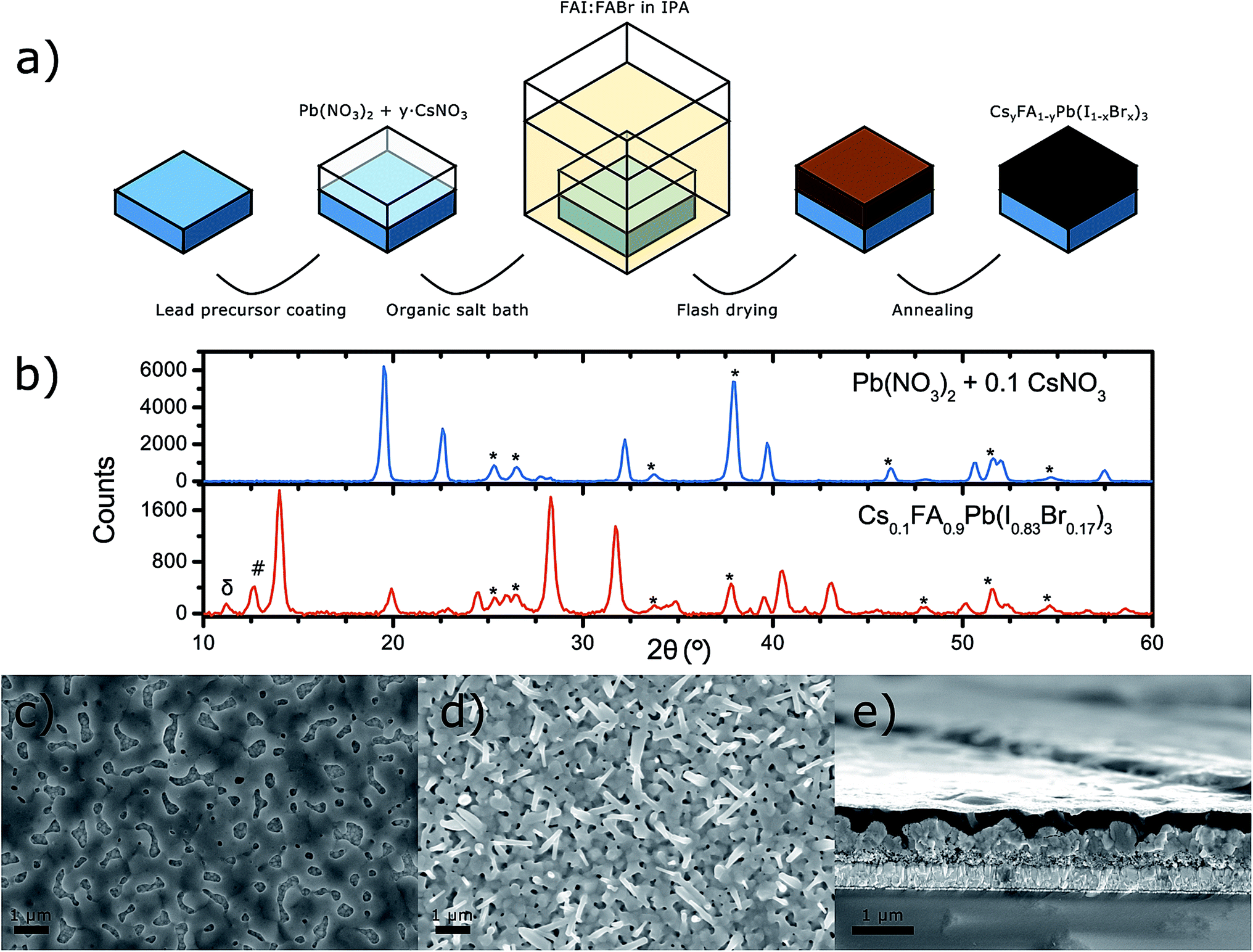 | ||
| Fig. 1 (a) Schematic illustration of the perovskite deposition process. (b) X-ray diffractograms of a metal nitrate precursor film as well as of the resulting perovskite film. The films were deposited on mp-TiO2 on FTO. The substrate, δ-perovskite phase and crystalline PbI2 signals are marked with *, δ and #, respectively. (c) Scanning electron-microscope images of the metal nitrate film surface, (d) the resulting perovskite film surface, (e) as well as a cross-section of a CsyFA1−yPb(IxBr1−x)3 solar cell. | ||
This reaction was favourable due to the low solubility of the inorganic nitrates and the resulting perovskite in IPA, compared to the high solubility of the FA-halide and FANO3. The samples were then removed from the organic halide bath, spin-dried and annealed to obtain the perovskite film. The neat perovskite films were then either characterised or processed further for solar cells. For the latter, a 2,2′,7,7′-tetrakis[N,N-di(4-methoxyphenyl)amino]-9,9′-spirobifluorene (spiro-OMeTAD) hole transport material (HTM) solution was spin-coated on the perovskite film and the devices were finalised by evaporating gold back contacts (see Experimental section for details).
Although the main topic of this study is the synthesis and analysis of formamidinium rich perovskites we also synthesised CsPbBr3 films on mesoporous TiO2 for fabrication of solar cells to demonstrate the compositional versatility of this technique. Without much optimisation we achieved a PCE of ∼3% for the CsPbBr3 solar cells (see ESI† for details). CsPbI3−xBrx perovskite films could essentially be synthesised in a similar manner to the technique we propose by controlling the composition of the halide precursor. This technique allows for a complete stoichiometric control of the precursors and, given the large solubility of CsNO3 in water, presents a convenient technique for synthesising CsPbBr3 films which, to date, have suffered from low film thickness because of the low solubility of CsBr in DMF and DMSO. However, methods employing a sequential deposition procedure for the CsPbBr3 have yielded success in increasing the perovskite film thickness.17,19
Material characterisation
The halide composition of the perovskite material was controlled by using stoichiometric amounts of the formamidinium iodide and formamidinium bromide salts in the dipping solution. Yang et al. have shown that the halide ratio in the dipping solution corresponds quite well to the ratio found in the perovskite formed from said solution.9 We employed a 83![[thin space (1/6-em)]](https://www.rsc.org/images/entities/char_2009.gif) :17 ratio of formamidinium iodide (FAI) and formamidinium bromide (FABr), respectively. This halide ratio has been shown to result in a very stable perovskite phase.35
:17 ratio of formamidinium iodide (FAI) and formamidinium bromide (FABr), respectively. This halide ratio has been shown to result in a very stable perovskite phase.35
In Fig. 1b, the X-ray diffractograms of the nitrate precursor film and of the resulting perovskite film, prepared from using a 10% molar ratio of CsNO3 to Pb(NO3)2 in water, are presented. The most characteristic XRD peaks for the lead nitrate could be observed at 19.5°, 22.5°, 32.2° and 39.7°. Caesium nitrate has a single dominant peak at 19.5° which completely overlaps with the diffraction peak of the lead nitrate. As shown in the ESI,† a larger amount of CsNO3 in the film resulted mostly in a sharp increase of the 19.5° peak. However, despite the 19.5° diffraction peak being the sharpest it is not the most convenient for confirming the presence of remnant nitrates in the perovskite film obtained after dipping the metal nitrate film into the organic halide bath. This is because the organic lead halide perovskite has a peak around 20° and the resolution limits of the instrument made it difficult to resolve those two peaks. The same applies for the diffraction peaks observed at 32.2° and 39.7°. At 22.5° there was a diffraction peak from the nitrate film that could possibly also be observed at 22.9° in the perovskite film. However, such small peaks could also result from impurities, insufficient amorphous background correction or noise in the instrument. Thus, from the XRD measurements we could neither confirm nor deny the presence of lead nitrate in the perovskite film with absolute certainty. In the XRD pattern of the Cs0.1FA0.9Pb(I0.83Br0.17)3 perovskite film, the most dominant characteristic perovskite peaks were observed at 14°, 19.9°, 28.3°, 31.8°, 40.5° and 43.1°. Below the main perovskite peak at 14° one could also observe two smaller peaks at 11.1° and 12.6° belonging to the δ-perovskite phase and PbI2, respectively.11
The metal nitrate was distributed homogenously over the TiO2 substrate, as one can observe from the scanning electron microscopy (SEM) image in Fig. 1c, but there was a considerable number of voids in the film. This was also observed by Hsieh et al.34 albeit the uncovered areas were much larger in their case. The resulting perovskite film obtained after dipping the metal nitrate precursor film into the organic halide bath fully covered the TiO2 substrate as shown in Fig. 1d. However, the perovskite film appeared to be porous due to the poor interconnection between the randomly oriented crystals it consists of. The shape of the perovskite crystals was that of needles and cuboids with micrometre length and width in the order of hundreds of nanometres. Furthermore, the SEM cross-section of a CsyFA1−yPb(IxBr1−x)3 solar cell in Fig. 1c also shows that the perovskite layer comprises of poorly connected crystal grains which resulted in a film with an uneven surface. It is also visible that the HTM permeates through the gaps in the perovskite layer, which puts the device at risk of short circuiting.
We also performed hard X-ray photoelectron spectroscopy (HAXPES), with a photon energy of 2100 eV at the KMC-1 beamline36 at BESSY II, on both the metal nitrate film and the resulting perovskite film deposited on FTO/TiO2 substrates and the results are presented in Fig. 2. Complete compositional characterisation of the perovskite surface can be found in the ESI.† It should be noted that the precursor sample spectrum may contain effects from differential charging in the order of 0.4–1.0 eV making a detailed analysis of the peak position, intensity and width somewhat ambiguous. However, it is clear from the results that the perovskite sample lacked features from the metal nitrate precursor. In the overview spectra (see Fig. 2a), one can observe the I 3d and I 4d peaks originating from the iodide content of the perovskite. Furthermore, two O 1s peaks and a Ti 2p peak (458.9 eV) can be observed in the precursor spectrum but not in the perovskite spectrum.37 In Fig. 2b we have enhanced the region of the O 1s peaks. It can be observed that the precursor presented two distinct O 1s peaks, as mentioned above. The peak at 530.2 eV, along with the Ti 2p peak, can be assigned to the mesoporous TiO2 substrate.38 This indicates that the precursor film does not uniformly cover the substrate, as is apparent also from the SEM image in Fig. 1c. No such signals were observed in the perovskite film spectra. The position of the second O 1s peak for the precursor (533 eV) is characteristic for oxygen atoms in a nitrate anion.39 For the perovskite film, only a single weak O 1s peak was observed in this binding energy region. The O 1s signal intensity in the perovskite film is of the same magnitude as for perovskite films manufactured without the use of metal nitrates. A comparison of the O 1s signal between a perovskite film synthesised with metal nitrate precursors and a perovskite film synthesised with conventional lead halide precursors is presented in Fig. S5.†
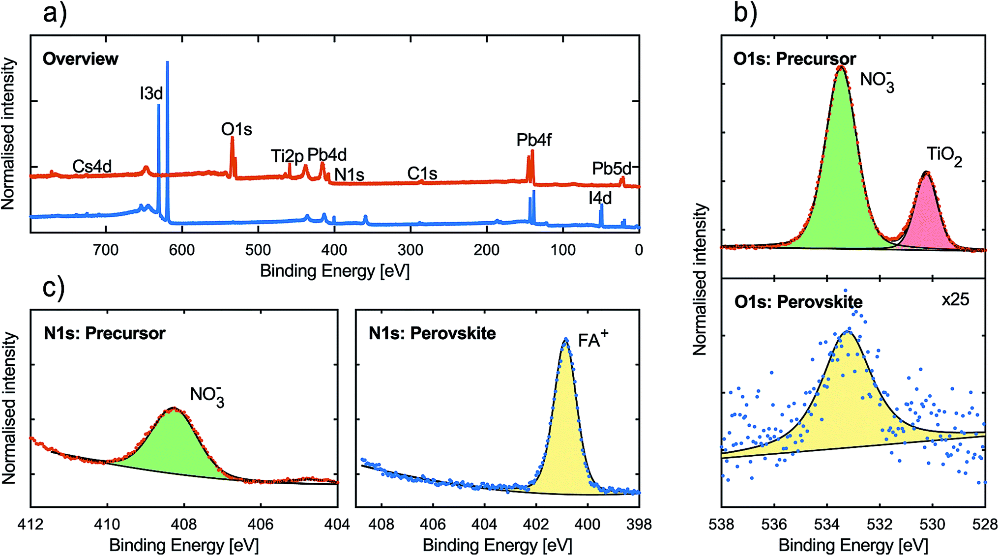 | ||
| Fig. 2 (a) Overview spectra of precursor (top) and perovskite (bottom), important peaks are labelled and the scale is normalised against the Pb 4f peak height. (b) O 1s spectra for the precursor and perovskite films. (c) N 1s spectra of the precursor and perovskite films. The O 1s and N 1s spectra are normalised against the Pb 4f peak area. | ||
The N 1s binding energy region was also measured in detail and the results are presented in Fig. 2c. For the metal nitrate precursor film spectrum, a peak is present at 408 eV, which corresponds to the nitrogen of the nitrate anion.39 In the perovskite film spectrum, this peak was not present but instead a large peak at a considerably lower energy (401 eV) was observed. This peak can be attributed to the nitrogen atom in the formamidinium ion.40 In general, the results from the HAXPES measurements indicate that the conversion of the metal nitrate precursor to perovskite was complete and that very little, if any, NO3− remained in the surface layer of the perovskite.
To confirm the insertion of the caesium and formamidinium cations into the perovskite we prepared a series of CsyFA1−yPbX3 films on FTO substrates (X = Br−, I− and y = 0, 0.1 and 0.2) all of which were studied using XRD and EDS. Lee et al.15 presented that the perovskite does not form stable alloys with more than 20% caesium, and similarly we were unable to synthesise stable perovskites with a larger caesium content. Because the resolution of EDS is roughly 150 eV, due to detector limitations, some characteristic elemental X-ray energies can overlap to such an extent that the stoichiometric analysis can easily fail. The bromide perovskites were analysed specifically because the signal for the characteristics Lα X-rays from caesium (4.286 keV) overlaps to a significant extent with the signal of Lα rays from iodine (3.937 keV). This makes the elemental evaluation of the bromide perovskites more accurate than of the iodide perovskites. We abstained from depositing these perovskite films on TiO2 substrates due to the Kα rays from titanium (4.508 keV) also overlapping with the caesium signal. The full X-ray diffractograms, energy dispersive spectra and the resulting elemental maps of the perovskite films, including the nitrate precursor films, can be found in the ESI.†
The EDS maps of the nitrate perovskite precursor film show that the caesium is homogenously distributed in the film and that no large phase separated regions are observed. Interestingly, the qualitative elemental ratio between lead and caesium, in both the precursor and the perovskite films, almost always results in a 5% underestimate of the expected caesium content in the film. This is consistent with our results from the HAXPES measurements on Cs0.1FA0.9Pb(I0.83Br0.17)3 perovskite films (see ESI†). We note that although there appears to be decrease in the Cs/Pb ratio when going from the precursor film to the perovskite, this could be because of slight unintended compositional differences from film to film. It is possible that the actual caesium amount in the film was lower than expected, but one should also consider that caesium does not exhibit a strong signal in the EDS measurement, as opposed to lead. This means that there could be a larger probability for error in evaluating the amount of caesium compared to the amount of lead.
The X-ray diffractograms of the perovskite films, enhanced to the region where the first characteristic perovskite diffraction peaks are observed, can be observed in Fig. 3a. The CsyFA1−yPbI3 perovskites have peaks around 13.8° and the CsyFA1−yPbBr3 perovskites have peaks around 14.7°. Although the exact peak positions could not be determined with greater accuracy, due to resolution limits of the instrument, a clear shift of the perovskite peak towards higher angles was observed with higher caesium content in the perovskite. This is consistent with the results from Lee et al.15 and suggests a contraction of the crystal lattice, which is logical since the ionic radius of caesium is smaller (1.67 Å) than that of formamidinium (2.53 Å).11
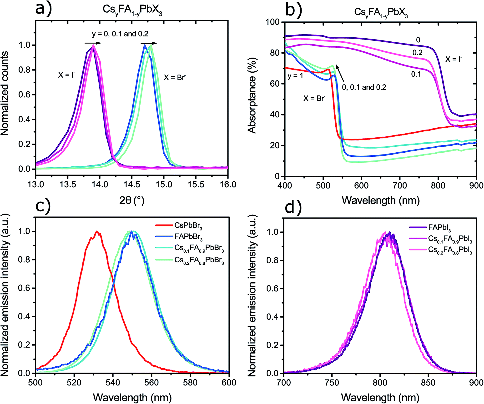 | ||
| Fig. 3 (a) X-ray diffractograms of the first peak for CsyFA1−yPbX3 perovskite films, where y = 0, 0.1, 0.2 and X is I− or Br−. (b) UV-vis absorptance spectra of the above-mentioned films as well as for pure CsPbBr3. (c) Transient photoluminescence spectra of the bromide perovskite films, (d) and of the iodide perovskite films. The presented photoluminescence spectra are the averages of 10 measurements to improve the signal to noise ratio. | ||
In Fig. 3b–d one can observe how the perovskite band-gap could be tuned by compositional control of the cations and anions. The inclusion of caesium into the FAPbX3 perovskites resulted in an increase of the band-gap of the material as seen by the shift of the absorption shoulders in Fig. 3b. For the bromide perovskites the shift in the band-gap can easily be seen from the characteristic excitonic peak which has peak position at around 530 nm, 525 nm, 523 nm, and 512 nm for perovskites containing 0, 10%, 20%, and 100% caesium to lead, respectively. The iodide perovskites show a similar trend where the absorption shoulders are positioned at around 785 nm, 780 nm and 775 nm for perovskites containing 0, 10% and 20% caesium to lead amount, respectively. Full transmittance and reflectance spectra of these films, in addition to their metal nitrate precursor films, can be found in the ESI.†
The transient photoluminescence spectra of the perovskite films, measured 15 ns after excitation in a nanosecond laser setup, also show a consistent increase of the band-gap with an increased caesium content as can be observed in Fig. 3c and d. The caesium addition resulted in a shift of the emission wavelength to higher energies and it was possible to observe that the overall curves were blue-shifted despite the absolute peak position differences were somewhat difficult to evaluate. The bromide perovskites were excited at 470 nm, which resulted in peak emission at around 550 nm for FAPbBr3, see Fig. 3c. Greater caesium content in the perovskite shifted the whole emission curve to lower wavelengths to a minimum of 530 nm for pure CsPbBr3. The iodide perovskites in Fig. 3, excited at 620 nm, emitted with a peak of around 810 nm for FAPbI3 which shifted down to shorter wavelengths by approximately 5 nm with 20% added caesium content. The steady-state photoluminescence of these samples showed a similar trend (see ESI†) but with somewhat different peak shapes due to possible detection limits of the instrument.
Photovoltaic properties of the solar cells
For optimisation of the solar cells we chose to focus on the perovskite composition of Cs0.1FA0.9Pb(I0.83Br0.17)3, since similar compositions have previously been shown to result in efficient and stable solar cells.15,18,35 In a two-step solution-based perovskite deposition procedure there are a multitude of parameters which can be controlled and optimised. Arguably, the three most important for the solar cell performance are: the precursor film thickness, dipping solution concentration and dipping time. The foremost parameter affects the final perovskite layer thickness and the latter two affect the perovskite crystallisation dynamics.To adjust the perovskite film thickness, and thus the amount of the active material on each solar cell, we tuned the concentration of the aqueous lead and caesium nitrate precursor solution (Cpre) over a range of 1.00–2.00 M with respect to Pb(NO3)2. The device performances, where the precursor concentration was varied, of a total of 38 solar cells is presented in Table 1. It should be noted that in the cases where statistics of JV parameters are presented, the solar cells are measured at a scan speed of 50 mV s−1 and scanned from open-circuit (OC) to short-circuit (SC) conditions. Champion devices were also measured at a scan speed of 10 mV s−1 and their hysteresis was taken into account by averaging the forward (SC to OC) and backwards (OC to SC) JV scans. As can be seen from Table 1, the devices prepared with 1.50 M and 1.75 M nitrate precursor solutions showed quite similar performance and the highest power conversion efficiencies (PCE) of all the concentrations tested. When scanned slowly, the champion solar cell for 1.50 M nitrate precursor solution gave a short-circuit current density (Jsc) of 18.8 mA cm−2, an open-circuit voltage (Voc) of 0.96 V and with a fill factor (FF) of 0.66 it yielded a PCE of 11.7% (see JV curve in ESI†).
:FABr 83:17 in IPA for 90 min. A total of 38 devices were measured
| C pre (M) | V oc (V) | J sc (mA cm−2) | FF | PCE (%) |
|---|---|---|---|---|
| 1.00 | 0.68 ± 0.13 | 5.3 ± 1.0 | 0.44 ± 0.09 | 1.6 ± 0.7 |
| 1.25 | 0.76 ± 0.17 | 14.1 ± 1.4 | 0.52 ± 0.09 | 5.8 ± 2.2 |
| 1.50 | 0.96 ± 0.01 | 20.0 ± 0.5 | 0.64 ± 0.03 | 12.3 ± 0.7 |
| 1.75 | 0.97 ± 0.01 | 19.3 ± 1.9 | 0.61 ± 0.03 | 11.6 ± 1.5 |
| 2.00 | 0.78 ± 0.29 | 7.9 ± 3.6 | 0.43 ± 0.07 | 3.0 ± 2.0 |
Proceeding from these results, the concentration of the organic halide salt dipping solutions (Cdip) was now varied. Below a dipping concentration of around 30 mM the perovskite crystallisation in the bath proved to be slow, i.e. in the order of hours. The films which were removed from these low Cdip baths after 90 min turned from brown to yellow immediately upon drying and did not convert to the light active perovskite phase upon heating. Long dipping times are not appealing for upscaling and there is also a greater potential for oxidation of the iodine, which in turn can cause degradation of the perovskite film, if the dipping bath is left in prolonged exposure to ambient air. High Cdip, ≥60 mM, resulted in an expedited iodine oxidation and despite a fast initial perovskite formation the films were degraded and yellow after a 90 min dipping time.
Since using a dipping solution concentration of 40 mM previously resulted in positive results, solar cells were fabricated using a range of different dipping solution concentrations, from 30 mM to 55 mM, and the results are presented in Table 2. As can be observed the performances of these devices were rather similar but the current output of the solar cells gradually decreased with Cdip larger than 40 mM, presumably because of degradation of the perovskite in the bath.
:FABr 83:17 in IPA for 90 min. A total of 76 devices were measured
| C dip (mM) | V oc (V) | J sc (mA cm−2) | FF | PCE (%) |
|---|---|---|---|---|
| 30 | 0.74 ± 0.07 | 17.2 ± 1.6 | 0.45 ± 0.07 | 5.7 ± 1.8 |
| 40 | 0.79 ± 0.02 | 17.4 ± 1.8 | 0.52 ± 0.02 | 7.2 ± 0.9 |
| 45 | 0.73 ± 0.07 | 15.2 ± 3.6 | 0.43 ± 0.05 | 4.9 ± 1.8 |
| 50 | 0.83 ± 0.03 | 15.6 ± 2.4 | 0.47 ± 0.07 | 6.2 ± 1.4 |
| 55 | 0.82 ± 0.02 | 9.1 ± 2.0 | 0.51 ± 0.03 | 3.8 ± 0.9 |
The third parameter to be optimised was the dipping time (tdip) of the precursor film in the organic halide salt solution. The previously used 90 min dipping time had been arbitrarily chosen to attempt to fully convert the lead nitrate to its perovskite or halide constituent. However, as clearly demonstrated in Table 3, this did not result in the most efficient solar cells. In fact, the shortest dipping times tested (10 min) proved on average to yield the best performing devices. Interestingly, the Voc of the solar cells gradually decreased as the dipping time was extended. Possibly, this was caused by excessive crystal growth that ultimately leads to an uneven perovskite surface that is likely to cause a greater amount of recombination in the devices.
:FABr 83:17 in IPA with a Cdip of 40 mM. A total of 67 devices were measured
| t dip (min) | V oc (V) | J sc (mA cm−2) | FF | PCE (%) |
|---|---|---|---|---|
| 10 | 1.01 ± 0.01 | 19.9 ± 1.9 | 0.64 ± 0.02 | 12.8 ± 1.2 |
| 20 | 0.99 ± 0.01 | 19.9 ± 2.1 | 0.64 ± 0.02 | 12.5 ± 1.4 |
| 30 | 0.95 ± 0.03 | 19.7 ± 2.7 | 0.63 ± 0.03 | 11.9 ± 2.0 |
| 45 | 0.95 ± 0.02 | 20.0 ± 1.6 | 0.64 ± 0.03 | 12.1 ± 1.1 |
| 60 | 0.93 ± 0.03 | 20.2 ± 1.4 | 0.64 ± 0.02 | 12.0 ± 1.3 |
| 75 | 0.90 ± 0.03 | 19.4 ± 1.2 | 0.59 ± 0.02 | 10.4 ± 1.0 |
Despite 10 min dipping being the best on average, the champion solar cell was obtained by dipping the nitrate precursor film in the organic halide salt solution for 30 min and its JV curves is presented in Fig. 4. As can be observed, there was some difference in the JV curve depending on the scan speed. For the backwards scan with a speed of 50 mV s−1 we obtained a PCE of 14.4% but with a speed of 10 V s−1 in the same direction we obtained a PCE of 13.4%. The 10 mV s−1 scans showed a considerably lower shunt resistance compared with the faster scan. This suggests that there is a recombination problem in the solar cell. Since the dark current scan shows that the device does not start conducting till above around 700 mV we do not believe the TiO2 layers to be the cause of recombination. It is more likely to be the result of an uneven perovskite film surface and possible pin-holes in the film. Despite these recombination issues the device exhibited an appreciably low hysteresis when scanned with 10 mV s−1 in both directions, yielding an average Voc of 0.96 V, a Jsc of 21.0 mA cm−2, a FF of 0.65 and a PCE of 13.0%. The maximum power point (MPP) tracking of the champion solar cell is also presented in Fig. 4. Following the MPP, a rather quick decrease in the PCE can be observed followed by stabilisation at around 8%. Similar trends have been observed in PSCs before and may be hysteresis related.5,17,20,22,29 It has been postulated that the hysteresis in PCSs most likely originates from ion-migration in the material and/or recombination rate differences at the perovskite interfaces.41,42 Therefore, through careful optimisation of these devices, the perovskite film quality and the hole and electron contacts, it is believed that the hysteresis issue of also the water-based PSC devices can be addressed.
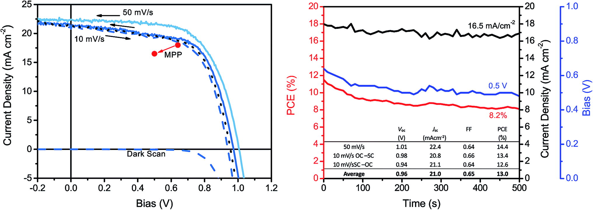 | ||
| Fig. 4 (Left) JV-curve of a champion solar cell, prepared with 1.5 M metal nitrate solution and dipped in 40 mM FAI:FABr solution for 30 min, with scan-speeds of 10 and 50 mV s−1. (Right) MPP tracking of the champion solar cell for 500 s as well as the tabulated JV-parameters from the JV-curve. | ||
We also tested solar cells with a different perovskite composition by varying the caesium content in the aqueous nitrate precursor solution, the results of which are presented in Table 4. As can be observed, fairly good devices can be prepared using 20% caesium nitrate. Perovskites with larger caesium content proved to be unstable as mentioned above, and the films were, therefore, not processed to solar cells. Also, devices prepared without caesium did not result in stable working devices.
| Cs (%) | t dip (min) | V oc (V) | J sc (mA cm−2) | FF | PCE (%) |
|---|---|---|---|---|---|
| 10 | 10 | 0.94 ± 0.10 | 19.5 ± 2.1 | 0.62 ± 0.07 | 11.3 ± 2.2 |
| 20 | 20 | 0.93 ± 0.06 | 18.5 ± 2.0 | 0.55 ± 0.08 | 9.6 ± 2.6 |
| 30 | 0.85 ± 0.04 | 19.0 ± 0.76 | 0.63 ± 0.04 | 10.2 ± 1.3 |
Conclusions
To summarise, an aqueous solution of caesium(I) nitrate and lead(II) nitrate was used to form a film, which then was dipped in an organic halide isopropanol bath to yield an inorganic/organic mixed-ion perovskite material. This is the first time that such a material is synthesised with a two-step method and without using any hazardous organic solvents. In this study, we prepared several different CsyFA1−yPb(I1−xBrx)3 perovskite materials using the above-mentioned technique. We found that the materials formed uniformly and did not result in a phase separation of two, or more, different perovskite materials. The material characterisation confirmed the inclusion of the caesium cation in the perovskite structure. By using hard X-ray photoelectron spectroscopy, we observed no residual nitrates in the surface region of the perovskite, which strongly hints at a complete conversion of the metal nitrate film. Our champion solar cell, which had a composition from synthesis of Cs0.1FA0.9Pb(I0.83Br0.17)3, presented a power conversion efficiency of 13.0%. With optimisation of the perovskite crystal growth, and with post-treatment of the surface layer, further improvements of the solar cell performance can be achieved. Our technique presents an opportunity to synthesise many different perovskite materials with a large compositional variety and complete compositional control. One could, for example, add rubidium(I) nitrate to the aqueous solution and form the famous quadruple cation perovskite or opt for fully inorganic perovskites. The versatility of the technique makes it relevant for large-scale manufacturing and paves the way for commercialisation of perovskite solar cells.Experimental
Solar cell preparation
Conducting fluorine doped tin(IV) oxide, SnO2:F, glass substrates (TEC15, Pilkington) were sectioned into squares of 15 × 25 mm2. A small strip along the longer edge of the substrate was then treated with zinc powder and 2 M HCl(aq) to chemically etch the conducting layer. The substrates were then cleaned in an ultrasonic bath using a 2% RBS-50 (Sigma) solution for 30 min followed by deionised water, acetone and ethanol for 15 min each. After cleaning, the substrates were dried using compressed air and a dense layer of TiO2 was spray-pyrolysed onto the substrate, using a solution of titanium(IV) tetraisopropoxide and acetylacetone in isopropanol, at a temperature of 500 °C. After cooling down, the TiO2 substrates were completed by spin-coating a 20 nm-diameter-TiO2-nanoparticle solution (150 mg paste, 18NRT, Dyesol, in 1 ml ethanol) at a rate of 3000 rpm for 10 s followed by drying for 15 min on a hotplate at 125 °C and annealing for 30 min on a hotplate at 500 °C.
For the perovskite synthesis, we dissolved lead(II) nitrate (99%, Sigma) in deionised water to prepare a 1.5 M Pb(NO3)2(aq) solution. At this stage, in order to synthesise an inorganic perovskite, caesium(I) nitrate (99,9%, Sigma) was also dissolved in the solution in the respective Cs/Pb molar ratio required. This solution was then spin-coated directly onto the UV-ozone cured (30 min) substrates, with and without TiO2, at 5000 rpm for 10 s, resulting in a transparent film which was subsequentially dried at 70 °C for 30 min.
The perovskite precursor nitrate films were then dipped into a chemical bath containing either, or both, formamidinium iodide (Dyenamo) and formamidinium bromide (Dyenamo) dissolved in isopropanol (anhydrous, Sigma) in the relative molar ratio that was desired for the iodide/bromide ratio of the perovskite material. The best films were obtained by a 40 mM solution with 83:17 FAI:FABr and a dipping time of 10 min. The substrates were then quickly removed from the bath, flash-dried by spin-coating at 5000 rpm for 3 s and annealed on a hot plate at 100 °C for 10 min.
Neat CsPbBr3 perovskite films were prepared in a similar manner by dipping equimolar CsNO3 and Pb(NO3)2 films into solutions of 40 mM HBr (Sigma, 47 wt% in water) in isopropanol (unless otherwise stated) and annealing at 250 °C for 10 min.
Solar cell characterisation
The current–voltage characteristics of the solar cells were measured with a Keithley 2400 source meter. A solar simulator (Newport Solar Simulator, model 91160) equipped with a 300 W xenon arc lamp, providing 1000 W m−2 illumination intensity and AM 1.5 G spectral distribution, was used as a light source. The light intensity was calibrated using a certified reference silicon solar cell (Fraunhofer ISE). The solar cells were measured with a scan speed of 50 mV s−1 and 10 mV s−1 and a circular shadow mask (0.126 cm2) was used to define the active area of the device.Material characterisation
Grazing incidence X-ray diffraction (GIXRD) of the perovskite films was measured, to study the crystallographic properties of the material, with a Siemens D5000 θ–2θ diffractometer fitted with a parallel-plate Soller-slit collimator with a resolution of 0.3°, and with a Cu Kα1 (λ = 1.54056 Å) radiation hitting the sample at an angle (θ) of 2°. The XRD pattern of the material was measured over Bragg angles (2θ) from 5° to 60° with a step size of 0.1° and a scan speed of 2 s per step.The light absorption properties of the perovskite films were measured using a Perkin-Elmer Lambda 900 double-beam UV/vis/NIR spectrophotometer equipped with an integrating sphere and a Spectralon reflectance standard along with a Fluorolog-3 (Horiba Jobin Yvon, Model FL3-222) instrument to measure the steady-state photoluminescence (ssPL). In the ssPL, the emission signal was corrected to account for the wavelength dependent sensitivity of the instrument along with normalising the signal with a reference silicon diode to account for any power fluctuations of the light source during the measurement.
Scanning electron microscopy was performed using Zeiss LEO1530/1550 microscopes fitted with identical thermal field emission tips and secondary electron (SE) detectors. SE images of the surface morphology were recorded using accelerator voltages of 3, 5 or 10 kV. Cross sectional SE images were recorded with 3 kV acceleration voltage. Energy dispersive spectroscopy was performed in the LEO1550 microscope using a Oxford EDS detector (X-Max, 80 mm2) using an accelerator voltage of 10 and 20 kV.
Transient photoluminescence spectroscopy
The measurements were performed with a laser flash photolysis spectrometer (Edinburgh Instrument LP920). Laser pulses were generated using a frequency tripled Nd:YAG laser (Continuum Surelight II, 10 Hz repetition rate, 10 ns pulse width) and tuned to the specific excitation wavelength in combination with an optical parametric oscillator (OPO, Continuum Surelight). The pulse intensity was attenuated to ∼1.8 mJ (with laser fluctuation estimated to be around 10%) per pulse using neutral density filters. The emission spectra were recorded with a CCD camera. The gate delay was set to be 15 ns, close to the limitation of the instruments.
X-ray photoelectron spectroscopy
X-ray photoelectron spectroscopy (XPS) was performed at the HIKE endstation at the KMC-1 beamline at BESSY II.36 A photon energy of 2100 eV was selected for the measurements using a double-crystal monochromator (Oxford-Danfysik) and the emitted electrons were detected using a Gammadata Scienta R-4000 hemispherical analyser. The perovskite and precursor samples were prepared at Uppsala University, and then sealed in a dark, low moisture atmosphere for about a week before being transferred into pressures lower than 10 mbar for measurement. The binding energy of all measurements was calibrated against the Au 4f peak of a gold foil mounted on the manipulator in electrical contact with the sample. The precursor sample may have contained some differential charging with broad and shifted Pb(NO3)2 peaks and as indicated by an advantageous carbon peak at 285.5 eV compared to 249.9 eV in the perovskite sample. The perovskite core levels were fitted with Voigt functions for quantification. The relative concentrations of the perovskite were determined by dividing the area of the fitted Voigt function with photoionisation cross section and normalising against the Pb 4f peak concentration.43Conflicts of interest
There are no conflicts to declare.Acknowledgements
We acknowledge financial support from the Göran Gustafsson Foundation, Swedish Energy Agency, ÅForsk, FORMAS, Swedish Foundation for Strategic Research, the Swedish Research Council (VR) and the Solar-era.net project “CNT-PV”. Dr Nan Kyi Kyi Thein also thanks the LOTUS+ program from Erasmus Mundus for a scholarship. We thank Michael Sturm for his laboratory assistance with initial perovskite synthesis and Fredrik Johansson and Dr Andreas Lindblad for help with the HAXPES measurements. The HIKE beamline is also acknowledged for the allocation of synchrotron radiation beamtime. We also thank Dr Jesper Jacobsson for providing a 1-step processed perovskite film for HAXPES measurements.References
- A. Kojima, K. Teshima, Y. Shirai and T. Miyasaka, J. Am. Chem. Soc., 2009, 131, 6050–6051 CrossRef CAS PubMed.
- J.-H. Im, C.-R. Lee, J.-W. Lee, S.-W. Park and N.-G. Park, Nanoscale, 2011, 3, 4088–4093 RSC.
- M. M. Lee, J. Teuscher, T. Miyasaka, T. N. Murakami and H. J. Snaith, Science, 2012, 338, 643–647 CrossRef CAS PubMed.
- H.-S. Kim, C.-R. Lee, J.-H. Im, K.-B. Lee, T. Moehl, A. Marchioro, S.-J. Moon, R. Humphry-Baker, J.-H. Yum, J. E. Moser, M. Grätzel and N.-G. Park, Sci. Rep., 2012, 2, 591 CrossRef PubMed.
- J. Burschka, N. Pellet, S.-J. Moon, R. Humphry-Baker, P. Gao, M. K. Nazeeruddin and M. Grätzel, Nature, 2013, 499, 316–319 CrossRef CAS PubMed.
- D. Liu and T. L. Kelly, Nat. Photonics, 2013, 8, 133–138 CrossRef.
- N. J. Jeon, J. H. Noh, Y. C. Kim, W. S. Yang, S. Ryu and S. Il Seok, Nat. Mater., 2014, 13, 897–903 CrossRef CAS PubMed.
- N. J. Jeon, J. H. Noh, W. S. Yang, Y. C. Kim, S. Ryu, J. Seo and S. Il Seok, Nature, 2015, 517, 476–480 CrossRef CAS PubMed.
- W. S. Yang, J. H. Noh, N. J. Jeon, Y. C. Kim, S. Ryu, J. Seo and S. Il Seok, Science, 2015, 348, 1234–1237 CrossRef CAS PubMed.
- M. Saliba, T. Matsui, J.-Y. Seo, K. Domanski, J.-P. Correa-Baena, M. K. Nazeeruddin, S. M. Zakeeruddin, W. Tress, A. Abate, A. Hagfeldt and M. Grätzel, Energy Environ. Sci., 2016, 9, 1989–1997 CAS.
- M. Saliba, T. Matsui, K. Domanski, J.-Y. Seo, A. Ummadisingu, S. M. Zakeeruddin, J.-P. Correa-Baena, W. R. Tress, A. Abate, A. Hagfeldt and M. Grätzel, Science, 2016, 354 DOI:10.1126/science.aah5557.
- W. S. Yang, B.-W. Park, E. H. Jung, N. J. Jeon, Y. C. Kim, D. U. Lee, S. S. Shin, J. Seo, E. K. Kim, J. H. Noh and S. Il Seok, Science, 2017, 356, 1376–1379 CrossRef CAS PubMed.
- N.-K. Kim, Y. H. Min, S. Noh, E. Cho, G. Jeong, M. Joo, S.-W. Ahn, J. S. Lee, S. Kim, K. Ihm, H. Ahn, Y. Kang, H.-S. Lee and D. Kim, Sci. Rep., 2017, 7, 4645 CrossRef PubMed.
- G. E. Eperon, S. D. Stranks, C. Menelaou, M. B. Johnston, L. M. Herz and H. J. Snaith, Energy Environ. Sci., 2014, 7, 982–988 CAS.
- J.-W. Lee, D.-H. Kim, H.-S. Kim, S.-W. Seo, S. M. Cho and N.-G. Park, Adv. Energy Mater., 2015, 1501310 CrossRef.
- Z. Li, M. Yang, J. S. Park, S. H. Wei, J. J. Berry and K. Zhu, Chem. Mater., 2016, 28, 284–292 CrossRef CAS.
- R. J. Sutton, G. E. Eperon, L. Miranda, E. S. Parrott, B. A. Kamino, J. B. Patel, M. T. Hörantner, M. B. Johnston, A. A. Haghighirad, D. T. Moore and H. J. Snaith, Adv. Energy Mater., 2016, 1502458 CrossRef.
- D. P. McMeekin, G. Sadoughi, W. Rehman, G. E. Eperon, M. Saliba, M. T. Horantner, A. Haghighirad, N. Sakai, L. Korte, B. Rech, M. B. Johnston, L. M. Herz and H. J. Snaith, Science, 2016, 351, 151–155 CrossRef CAS PubMed.
- M. Kulbak, D. Cahen and G. Hodes, J. Phys. Chem. Lett., 2015, 6, 2452–2456 CrossRef CAS PubMed.
- G. E. Eperon, G. M. Paterno, R. J. Sutton, A. Zampetti, A. A. Haghighirad, F. Cacialli and H. J. Snaith, J. Mater. Chem. A, 2015, 3, 19688–19695 CAS.
- J. Liang, C. Wang, Y. Wang, Z. Xu, Z. Lu, Y. Ma, H. Zhu, Y. Hu, C. Xiao, X. Yi, G. Zhu, H. Lv, L. Ma, T. Chen, Z. Tie, Z. Jin and J. Liu, J. Am. Chem. Soc., 2016, 138, 15829–15832 CrossRef CAS PubMed.
- M. Kulbak, S. Gupta, N. Kedem, I. Levine, T. Bendikov, G. Hodes and D. Cahen, J. Phys. Chem. Lett., 2016, 7, 167–172 CrossRef CAS PubMed.
- K. A. Bush, A. F. Palmstrom, Z. J. Yu, M. Boccard, R. Cheacharoen, J. P. Mailoa, D. P. McMeekin, R. L. Z. Hoye, C. D. Bailie, T. Leijtens, I. M. Peters, M. C. Minichetti, N. Rolston, R. Prasanna, S. Sofia, D. Harwood, W. Ma, F. Moghadam, H. J. Snaith, T. Buonassisi, Z. C. Holman, S. F. Bent and M. D. McGehee, Nat. Energy, 2017, 2, 17009 CrossRef CAS.
- S. Aharon, B. Cohen and L. Etgar, J. Phys. Chem. C, 2014, 118, 17160–17165 CAS.
- S. A. Kulkarni, T. Baikie, P. P. Boix, N. Yantara, N. Mathews and S. Mhaisalkar, J. Mater. Chem. A, 2014, 2, 9221 CAS.
- H. Chen, X. Zheng, Q. Li, Y. Yang, S. Xiao, C. Hu, Y. Bai, T. Zhang, K. S. Wong and S. Yang, J. Mater. Chem. A, 2016, 4, 12897–12912 CAS.
- M. Lv, X. Dong, X. Fang, B. Lin, S. Zhang, J. Ding and N. Yuan, RSC Adv., 2015, 5, 20521–20529 RSC.
- W. Nie, H. Tsai, R. Asadpour, J.-C. Blancon, A. J. Neukirch, G. Gupta, J. J. Crochet, M. Chhowalla, S. Tretiak, M. A. Alam, H. Wang and A. D. Mohite, Science, 2015, 347, 522–525 CrossRef CAS PubMed.
- K. L. Gardner, J. G. Tait, T. Merckx, W. Qiu, U. W. Paetzold, L. Kootstra, M. Jaysankar, R. Gehlhaar, D. Cheyns, P. Heremans and J. Poortmans, Adv. Energy Mater., 2016, 6, 1–8 Search PubMed.
- D. M. Wood, A. D. Brailsford and P. I. Dargan, Drug Test. Anal., 2011, 3, 417–425 CrossRef CAS PubMed.
- R. B. Palmer, Toxicol. Rev., 2004, 23, 21–31 CrossRef CAS PubMed.
- R. E. Beal, D. J. Slotcavage, T. Leijtens, A. R. Bowring, R. A. Belisle, W. H. Nguyen, G. Burkhard, E. T. Hoke and M. D. McGehee, J. Phys. Chem. Lett., 2016, 746–751 CrossRef CAS PubMed.
- N. K. Noel, S. N. Habisreutinger, B. Wenger, M. T. Klug, M. T. Hörantner, M. B. Johnston, R. J. Nicholas, D. T. Moore and H. J. Snaith, Energy Environ. Sci., 2017, 10, 1–15 Search PubMed.
- T.-Y. Hsieh, T.-C. Wei, K.-L. Wu, M. Ikegami and T. Miyasaka, Chem. Commun., 2015, 51, 13294–13297 RSC.
- K. A. Bush, A. F. Palmstrom, Z. J. Yu, M. Boccard, R. Cheacharoen, J. P. Mailoa, D. P. McMeekin, R. L. Z. Hoye, C. D. Bailie, T. Leijtens, I. M. Peters, M. C. Minichetti, N. Rolston, R. Prasanna, S. Sofia, D. Harwood, W. Ma, F. Moghadam, H. J. Snaith, T. Buonassisi, Z. C. Holman, S. F. Bent and M. D. McGehee, Nat. Energy, 2017, 2, 17009 CrossRef CAS.
- F. Schaefers, M. Mertin and M. Gorgoi, Rev. Sci. Instrum., 2007, 78, 123102 CrossRef CAS PubMed.
- K. Westermark, A. Henningsson, H. Rensmo, S. Sodergren, H. Siegbahn and A. Hagfeldt, Chem. Phys., 2002, 285, 157–165 CrossRef CAS.
- R. Knut, R. Lindblad, S. Grachev, J. Y. Faou, M. Gorgoi, H. Rensmo, E. Søndergard and O. Karis, J. Appl. Phys., 2014, 115, 43714 CrossRef.
- R. G. Coppertahwaite, S. Afr. J. Chem., 1983, 36, 125–129 Search PubMed.
- B. Philippe, M. Saliba, J. P. Correa-Baena, U. B. Cappel, S. H. Turren-Cruz, M. Grätzel, A. Hagfeldt and H. Rensmo, Chem. Mater., 2017, 29, 3589–3596 CrossRef CAS.
- H. J. Snaith, A. Abate, J. M. Ball, G. E. Eperon, T. Leijtens, N. K. Noel, S. D. Stranks, J. T. W. Wang, K. Wojciechowski and W. Zhang, J. Phys. Chem. Lett., 2014, 5, 1511–1515 CrossRef CAS PubMed.
- W. Tress, N. Marinova, T. Moehl, S. M. Zakeeruddin, M. K. Nazeeruddin and M. Grätzel, Energy Environ. Sci., 2015, 8, 995–1004 CAS.
- J. H. Scofield, Theoretical Photoionization Cross Sections from 1 to 1500 keV, University of California, Livermore, California, 1973 Search PubMed.
Footnote |
| † Electronic supplementary information (ESI) available: Cs1−yFAyPbI3 and Cs1−yFAyPbBr3 XRD, UV-vis transmittance/reflectance, PL spectra, EDS and characterization of perovskite films for solar cell optimization. Additional HAXPES and CsyFA1−yPb(IxBr1−x)3JVs. CsPbBr3JV data. See DOI: 10.1039/c7se00538e |
| This journal is © The Royal Society of Chemistry 2018 |