
Evaluating spinel ferrites MFe2O4 (M = Cu, Mg, Zn) as photoanodes for solar water oxidation: prospects and limitations†
N.
Guijarro
 *,
P.
Bornoz
,
M.
Prévot
,
X.
Yu
,
X.
Zhu
,
M.
Johnson
,
X.
Jeanbourquin
,
F.
Le Formal
and
K.
Sivula
*
*,
P.
Bornoz
,
M.
Prévot
,
X.
Yu
,
X.
Zhu
,
M.
Johnson
,
X.
Jeanbourquin
,
F.
Le Formal
and
K.
Sivula
*
Laboratory for Molecular Engineering of Optoelectronic Nanomaterials, École Polytechnique Fédérale de Lausanne (EPFL), Station 6, 1015 Lausanne, Switzerland. E-mail: nestor.guijarro@epfl.ch; kevin.sivula@epfl.ch
First published on 31st October 2017
Abstract
The search for ideal semiconductors for photoelectrochemical solar fuel conversion has recently recognized the spinel ferrites as promising candidates due to their optoelectronic tunability together with superb chemical stability. However, a systematic understanding of the main material factors limiting their performance is currently lacking. Herein, nanostructured thin-film electrodes of three representative spinels, namely CuFe2O4 (CFO), MgFe2O4 (MFO) and ZnFe2O4 (ZFO), are prepared by a solution-based approach and their photoelectrochemical (PEC) properties are comprehensively characterized. Annealing post-treatments together with the deposition of NiFeOx overlayers are found to improve the native n-type response, although a dominant bulk recombination (especially in MFO) limits the saturation photocurrents (below 0.4 mA cm−2 at 1.23 V vs. RHE). Likewise, prominent Fermi level pinning due to surface states at around 0.9 V vs. RHE in all cases appears to limit the photovoltage (to ca. 300 mV). Rapid-scan voltammetry is used to gain insight into the surface states and the operation of the overlayer. Interestingly, the NiFeOx is ineffective at mitigating Fermi level pinning, but clearly participates as an electrocatalyst to improve the overall performance. Generally, these results evidence the potential and current intrinsic limitations of the spinel ferrites—establishing a roadmap for the optimization of these materials as photoanodes for solar water oxidation.
Introduction
Solar-powered electrosynthesis using photoelectrochemical (PEC) cells is a promising avenue for producing commodity compounds such as hydrogen, hydrogen peroxide, methane and methanol for energy storage or chemical feedstocks.1–3 A promising PEC technology is the dual-absorber tandem PEC cell4 wherein two semiconducting photoelectrodes, which absorb complementary parts of the Sun's spectrum, are wired together to generate an overall photovoltage sufficient to drive the intended oxidation and reduction reactions, respectively, at the photoanode and photocathode. At the photocathode the production of hydrogen (reduction of water),5–9 H2O2 (reduction of O2),10 methane and methanol (reduction of CO2)11 has been demonstrated using this concept, whereas an oxidation reaction (usually oxygen evolution from water) occurs at the photoanode.Semiconducting metal oxides represent a promising class of photoanode material given their general durability under operation conditions and their facile processability via scalable solution-based routes.12 Indeed, research on first-generation binary oxides, viz. TiO2, WO3 and Fe2O3, has firmly established this class of materials as robust and active toward water oxidation, however, since none of the binary metal oxides satisfy all of the requirements for ideal application in a PEC device, research has shifted towards identifying promising ternary or multinary oxide semiconductors.13 The spinel ferrites (MFe2O4, M = Ba, Ca, Cu, Co, Mg, Mn, Ni, Zn) are an emerging family of metal oxides that has recently drawn increasing attention for solar energy conversion applications.14 Their attractiveness is underpinned by remarkable thermal and chemical stabilities and the tunability of the band gap energy (1.4–2.7 eV) by selecting the M2+ cation. Several studies have demonstrated the robustness and potential for water photooxidation of these materials.15–18 In particular the deposition of spinel ferrite thin-film overlayers onto conventional metal oxide photoanodes has shown enhanced performance due to improved charge separation at the oxide heterojunction for the combinations of Fe2O3/CaFe2O4,19 Fe2O3/ZnFe2O4,20,21 TaON/CaFe2O4,22 and BiVO4/CaFe2O4.23 Despite this, comprehensive evaluation of the optoelectronic and PEC properties of the spinel ferrites themselves is lacking. Indeed, only a few reports have studied spinel ferrites alone as the principle photoactive material for water oxidation.16,24 Díez-García et al. reported that the PEC behaviour of a nanoparticulate CuFe2O4 electrode can be switched from photoanodic to photocathodic by an electrochemical stripping treatment,25 although very low photocurrents (<50 μA cm−2) were obtained in both cases. Tahir et al. described the fabrication of ZnFe2O4 thin-film electrodes by means of chemical vapour deposition at mild temperatures using a single organic precursor,26 whereas Bein and co-workers prepared macroporous thin-films of this material by atomic layer deposition (ALD) using a scaffold of antimony-doped tin oxide,27 resulting photoanodic currents of about 0.2 and 0.3 mA cm−2 at 1.23 V vs. RHE, respectively. Recently, Kim et al. proposed an innovative route for the fabrication of ZnFe2O4 thin-films based on the solid-state reaction between β-FeOOH and Zn(NO3)2 directly on the electrode with a rapid thermal annealing yielding photocurrents that rival or outperform those obtained with previously reviewed approaches.28,29 This methodology provides a pathway to circumvent the harsh annealing conditions required for the traditional solid-state reaction used to prepare spinel ferrites while also enabling solution-processing onto conventional transparent conductive substrates with commercially available precursors.
To comprehensively evaluate the potential for the spinel ferrites materials in light of the synthetic advance by Kim et al., herein we present a systematic study of the morphology, crystal-structure, optoelectronic properties, and faradaic efficiency for oxygen evolution of three different spinel ferrites (CuFe2O4, MgFe2O4 and ZnFe2O4). Overall, this work aims to identify the key parameters that limit the performance of ferrospinels as photoanodes for water oxidation, and to establish a clear roadmap to address these problems for implementation of this class of materials in PEC tandem cells.
Results and discussion
Optical properties, morphology and crystal structure of spinel ferrites thin-films
Three different spinel ferrites CuFe2O4 (CFO), MgFe2O4 (MFO) and ZnFe2O4 (ZFO) were chosen as model materials in this study. In all the cases the thin-film electrodes were prepared on transparent conducting oxide (FTO) substrates using a solution-based route similar to that reported by Kim et al.28 In brief, the rapid-annealing (800 °C, 20 min) of a chemical bath deposition (CBD) layer of β-FeOOH coated with an excess of the corresponding metal nitrate produced the spinel ferrite; the crust of binary metal oxide – CuO, MgO or ZnO, resulting from the excess of metal nitrate – was subsequently chemically etched to afford the pure spinel ferrite thin film. Different post-treatments viz. mild annealing under a hydrogen atmosphere or annealing at 550 °C for extended duration were also investigated to determine the effect of the preparation conditions on the optoelectronic properties (see Experimental methods section for full details).Fig. 1a displays the UV-Vis absorption spectra of the β-FeOOH precursor and the resulting spinel ferrites. The absorption onset red shifts by ca. 50 nm (MFO), 100 nm (ZFO) or 350 nm (CFO) with respect the β-FeOOH precursor. Further analysis of the optical characteristics using Tauc plots gives estimates for both indirect (Eig) and direct (Edg) and optical band gaps (Fig. 1b and c, respectively) that agree with previous reports.14 Specifically, CFO shows Edg = 1.9 eV and Eig = 1.3 eV, MFO exhibits broader Edg and Eig of about 2.4 eV and 2.0 eV, respectively, and ZFO shows Edg = 2.3 eV and Eig = 1.9 eV. It must be noted, however, that previous reports on different spinel ferrites have pointed out that light absorption via indirect transition does not effectively drive PEC processes.30
 | ||
| Fig. 1 Thin film UV-Vis absorption spectra of β-FeOOH, CuFe2O4, MgFe2O4 and ZnFe2O4 (a) and the corresponding Tauc plot analysis for the indirect optical band gap energy (b) and the direct optical band gap energy (c). | ||
The phase composition and crystal structure of the spinel ferrite thin-films were next examined by X-ray diffraction (XRD) and Raman spectroscopy. The diffractograms shown in Fig. 2a–c for the CFO, MFO, and ZFO, respectively, reveal peaks associated to the corresponding ferrite and the substrate, with no discernible signals for other segregated phases. It should be noted that for the normal spinel structure the M2+ and Fe3+ occupy the tetrahedral and octahedral sites respectively, whereas in an inverted spinel the M2+ occupy the octahedral sites of the structure and the Fe3+ are equally split between the octahedral and tetrahedral sites. The degree of inversion31 (i.e. the percentage of Fe3+ ions occupying tetrahedral sites) is known to affect the magnetic behaviour of the samples,32 but a link to PEC properties is not known.
 | ||
| Fig. 2 XRD and Raman spectra for CFO and 550-CFO (a, d) as well as as-prepared MFO (b, e) and ZFO (c, f). Detail of the (211) peak for CFO and 550-CFO is shown as an inset. Representative reference diffraction patterns were also included for the sake of the examination. Raman modes were assigned following the literature (see main text). | ||
The XRD of the as-prepared CFO film (black line Fig. 2a) displays only the reflections corresponding to the tetragonal ferrospinel structure with a space group of I41/amd, which typically corresponds to a “partially” inverse spinel ferrite.14,15 These results are in agreement with those reported by Tang et al. who demonstrated that the tetragonal phase was predominant in CFO at temperatures below 900 °C while a cubic phase develops at higher temperatures.33 Subsequent annealing treatment at 550 °C (550-CFO, green line) led to a distinct increase in intensity, as clearly evidenced for the (211) crystal plane (Fig. 2a, inset), which points to an improved crystallinity upon this post-treatment. The concomitant shift of the peak attributed to the (211) reflection is consistent with a contraction of the crystal lattice. The MFO and ZFO diffractograms (Fig. 2b and c) show that these materials crystallize in a cubic structure (Fd3m space group). In both cases, subsequent post-annealing treatment under hydrogen atmosphere at 200 °C did not affect to XRD patterns (results not shown) indicating that no change in the bulk crystal structure occurs, similar to results recently reported by Kim et al.28,29 Note that in the ZFO diffractogram the small pair of peaks located between 31–32 °C could be ascribed to small traces of maghemite (γ-Fe2O3 – JCPDS #39-1346) and magnetite (Fe3O4 – JCPDS #75-0033).34
To further confirm the crystal phase and the absence of secondary phases in the as-prepared thin-films, Raman spectra were collected (Fig. 2d–f). CFO displays a main band centred at 674 cm−1 ascribed to the A1g mode, and two weaker bands at 168 cm−1 and 483 cm−1 (broad) which have been assigned to Eg and F2g modes, respectively.35–37 Likewise, Raman spectra of MFO shows six bands at 223 cm−1 (F2g), 336 cm−1 (Eg), 482 cm−1 (F2g), 545 cm−1 (F2g) and 705.5 cm−1 (A1g) in good agreement with the values reported by Wang et al.38 Note that the mode at 633 cm−1 has been attributed to an order-disorder effect due to the inversion degree.38 The Raman spectrum of ZFO exhibits a weak feature at 243 cm−1 (Eg) followed by two three bands centred 348 cm−1 (F2g), 500 cm−1 (F2g) and 650 cm−1.39 Note that the latter appears to comprise two bands. The first one at 642 cm−1 clearly corresponds to the A1g mode in the ZFO, whereas the second could indicate the presence of traces of Fe3O4, whose Raman signature is similar to that of the ZFO,40 or be caused by defect states.41 Overall, in all cases the Raman spectra corroborate the presence of the spinel ferrite without parasitic phases. The absence of the characteristic signals of α-Fe2O3,42 CuO,43 ZnO,44 MgO,45 β-FeOOH,45 γ-Fe2O3 (ref. 46) and Fe3O4 (ref. 40) suggest the growth of monophasic spinel ferrite thin-films (except in the case of ZFO where the presence of traces of Fe3O4 or γ-Fe2O3 or cannot be ruled out completely).
X-ray Photoelectron Spectroscopy (XPS) was next used to verify the chemical states of the species that constitute the prepared spinel ferrite thin films. XPS survey spectra obtained for the different spinel ferrites confirms the presence of the main elements as well as adventitious carbon (Fig. S1, ESI†). High resolution XPS spectra for each element are shown in Fig. 3 for the samples after the post treatments (550 °C annealing for CFO (550-CFO) and annealing under hydrogen for MFO (H-MFO) and ZFO (H-ZFO)). In the case of CFO, the Cu 2p XPS spectrum shows the expected four signals associated with the presence of Cu2+. The binding energy of Cu 2p1/2 and Cu 2p3/2 at 951.0 eV and 933.2 eV together with the typical satellite peaks at 959.2 eV and 941.3 eV match with previous studies on CFO.47,48 Although the satellite signals confirm the existence of Cu2+, the presence of traces of metallic copper or Cu+ cannot be completely discarded since their Cu 2p1/2 and Cu 2p3/2 features would overlap with those of Cu2+.49 However, previous analysis by XRD does not suggest the presence of metallic copper or Cu2O. Close examination of the Mg 2p XPS spectrum for the MFO, reveals that the signal is composed of two bands located at 48.9 eV and 50.2 eV. Yan et al. attributed these signals to the presence of Mg2+ in different environments.50 The most intense signal at lower binding energy can be assigned to Mg2+ in tetrahedral sites, whereas the weaker signal could be linked to a partial migration of cations to octahedral sites or magnesium bonded to –OH groups.51 In the case of ZFO, the single band at 1021.0 eV for the Zn 2p3/2 signal confirms the divalent state of Zn within the material in agreement with previous reports.18
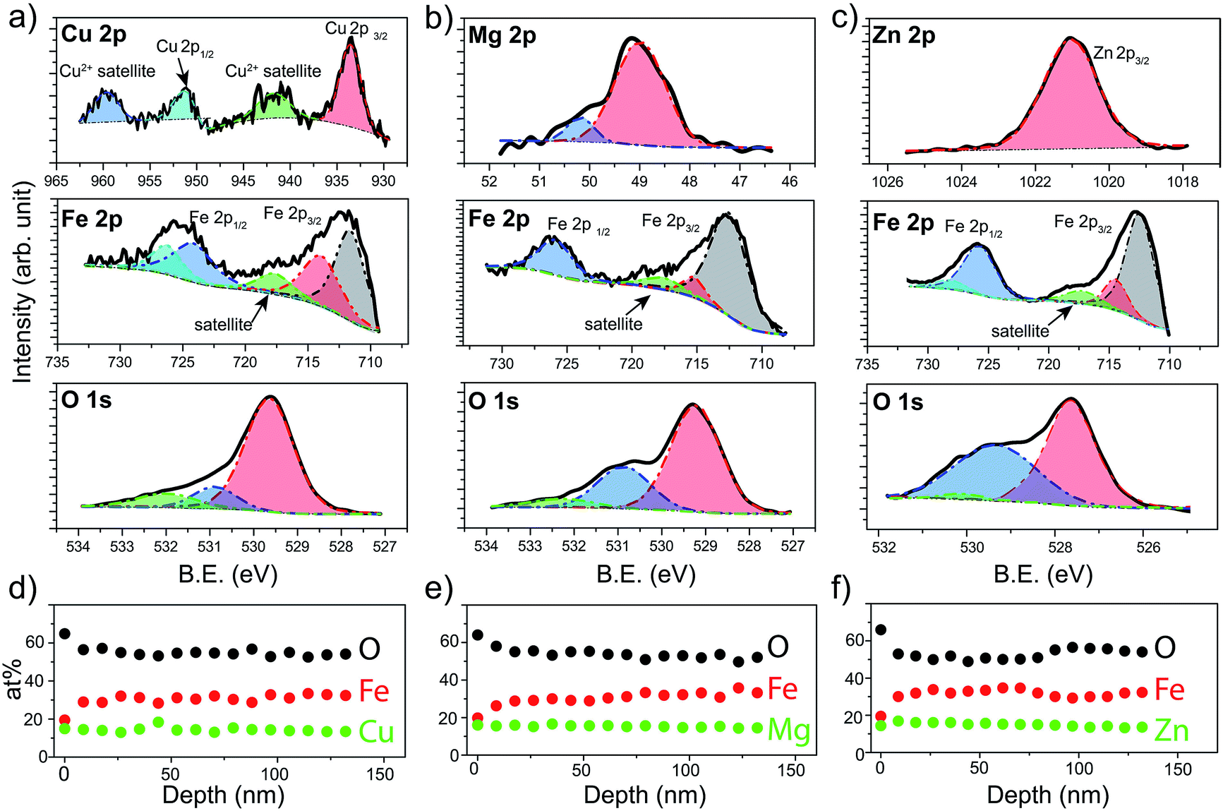 | ||
| Fig. 3 Binding energy (B.E.) narrow-scan XPS for 550-CFO (a), H-MFO (b) and H-ZFO (c) corresponding to the Cu 2p, Mg 2p and Zn 2p region, respectively, as well as, to Fe 2p and O 1s are shown. The deconvolution, fitting and baseline (Shirley) are included as dashed lines, see main text for the description. Atomic concentration (at%) of the metal, iron and oxygen as a function of the depth for the 550-CFO (d), H-MFO (e) and H-ZFO (f). | ||
The Fe 2p spectrum of the three spinels display the Fe 2p3/2 and Fe 2p1/2 peaks accompanied by a satellite signal at around 718 eV, which corroborates the presence of only Fe3+.52 Note that the Fe 2p3/2 peak can be deconvolved into two bands at approximately 711–712 eV (stronger) and 714–715 eV (weaker) consistent with Fe3+ cations in octahedral and tetrahedral sites, respectively, due to the partial inversion of the structures.50,53
Indeed, the relative intensities of these peaks clearly shows that the degree of inversion in CFO is higher compared to MFO or ZFO. Likewise, the contributions at around 724–727 eV were assigned to the chemical state Fe3+. Finally, O 1s spectra show a single band that can be deconvolved into three contributions suggesting three distinct environments for oxygen atoms.29 From lower to higher binding energy, the bands have been ascribed to the metal–oxygen bonds from the lattice (stronger contribution), defects of oxygen vacancies, and hydroxyl groups bonded to the metal (or adsorbed water) at the surface. It must be emphasized that the post-annealing treatments only cause noticeable changes in the O 1s spectra (see Fig. S2 for characterization of as-prepared samples, ESI†). In the case of CFO, there exists a significant decrease on the adsorbed water or hydroxyl groups linked to the 550 °C annealing for extended time. Likewise, in the case of ZFO and MFO, the annealing under hydrogen causes a noticeable increase of the oxygen vacancies, as expected for a mild annealing under reductive atmosphere.29
In order to analyze the distribution of the different species across the film thickness, XPS depth profiles were measured. Fig. 3d–f show the composition of the films as a function of the estimated depth. Interestingly, in all the cases the surface of the spinel ferrite appears to be M2+-rich and Fe3+-poor,29 reaching the stoichiometric composition (14.3% M: 28.6% Fe: 57.1% O) below 20 nm depth and remaining constant thereafter. The excess oxygen on the surface could be accounted for by the adsorbed water and hydroxyl groups. Apart from the elements that compose the spinel ferrite, traces of Sn (below 1 at%) have been also detected. This is not unexpected taking into account that annealing treatments above 700 °C are known to trigger the diffusion of Sn from the conductive substrate.54 Note that the Sn-doping has been reported to improve the PEC performance in hematite likely by Fe3+ substitution, and thus, its beneficial n-doping effect could not be ruled out.55
The morphology of the thin-films has demonstrated to be a key parameter governing the PEC response of photoanodes such as Fe2O3,56 BiVO4 (ref. 57) or Ta3N5.58 To shed some light into the nanoscopic structure of the spinel ferrites, the morphology was examined by collecting the SEM images. A top-view image of the precursor β-FeOOH film (Fig. S3, ESI†) reveals an array of nanorods, 30–50 nm in diameter, in agreement with the results reported by Hagfeldt and co-workers.59 Closer inspection of the nanorods by TEM evidenced their single-crystalline nature (Fig. S3, ESI†). Subsequent reaction with the corresponding metal nitrates lead to significant changes in the morphology of the thin-film. In the case of CFO, a top-view SEM image (Fig. 4a, top) shows an open structure formed by interconnected nanoparticles.
 | ||
| Fig. 4 Top-view (top) and cross-sectional (middle) SEM and TEM images (bottom) corresponding to 550-CFO (a), H-MFO (b) and H-ZFO (c). Colors in cross-sectional SEM are a guide to discern between the FTO substrate (blue) and the spinel ferrite grown on-top (red, yellow and orange, respectively). | ||
The cross-sectional image (Fig. 4a, middle) clearly shows particles of around 100–200 nm and a thickness of approximately 260 nm. A TEM image of the CFO particles scratched from the film (Fig. 4a, bottom) reflects the polycrystalline nature of the particles and shows lattice fringes that match with the (200), (103) and (211) lattice planes expected from the crystal structure. The top-view SEM image of MFO shows an uneven distribution of nanowires (and possibly nanoparticles) on the surface of the electrode, with a diameter of around 15–30 nm (Fig. 4b, top). The cross-sectional SEM image clearly shows that the network of nanowires (and nanoparticles) is intertwined with a film thickness of ca. 400 nm (Fig. 4b, middle). During the TEM characterization only polycrystalline nanoparticles with lattice spacing corresponding to the (220) and (311) lattice planes were observed (Fig. 4b, bottom). Finally, the top-view SEM image of ZFO resembles that of β-FeOOH exhibiting an array of ordered nanorods with a diameter of around 70 nm (Fig. 4c, top). It is worth mentioning that not only the diameter of the nanorods appears to increase (from around 40 nm in the β-FeOOH film), but also the shape appears with more rounded edges as Lee and co-workers reported previously.28 The cross-sectional image shows the vertical alignment of the ZFO nanorods and indicated that the film is approx. 320 nm thick (Fig. 4c, middle). Close inspection by TEM reflects the polycrystalline nature of the nanorods, with lattice spacing that matches with the (220) and (311) crystal planes (Fig. 4c, bottom). The M![[thin space (1/6-em)]](https://www.rsc.org/images/entities/char_2009.gif) :Fe ratio of the samples examined by TEM was determined with EDX obtaining values of 1:1.8 (Zn:Fe), 1:2.2 (Mg:Fe) and 1:2.1 (Cu:Fe) which agree with the stoichiometry of the materials and previously-discussed XPS results.
:Fe ratio of the samples examined by TEM was determined with EDX obtaining values of 1:1.8 (Zn:Fe), 1:2.2 (Mg:Fe) and 1:2.1 (Cu:Fe) which agree with the stoichiometry of the materials and previously-discussed XPS results.
To summarize the physical characterization of the spinel ferrite films, the solution-based route28 previously reported for ZFO has been shown to be suitable also for the fabrication of CFO and MFO. Combined information collected by XRD, Raman spectroscopy and XPS provided evidence of the formation of phase-pure spinel ferrites, albeit in the case of ZFO the presence of Fe3O4 could not be unequivocally discarded. In all the cases, XPS depth-profiling pointed out that the surface composition differs from the bulk, unveiling a metal-rich and iron-poor surface but a near-stoichiometric bulk. Interestingly, the morphology of the spinel ferrite appears to be strongly dependent on the metal. In the case of ZFO the initial layer of β-FeOOH seems to act as a template driving the crystallization of the spinel as a nanorod array, whereas thin-films formed by randomly packed nanowires or fused-nanoparticles were obtained for MFO and CFO, respectively. We next address the study of the PEC properties bearing in mind that the optical properties, crystallinity, composition, and morphology of these films will affect the performance for water photooxidation.
Photoelectrochemical characterization
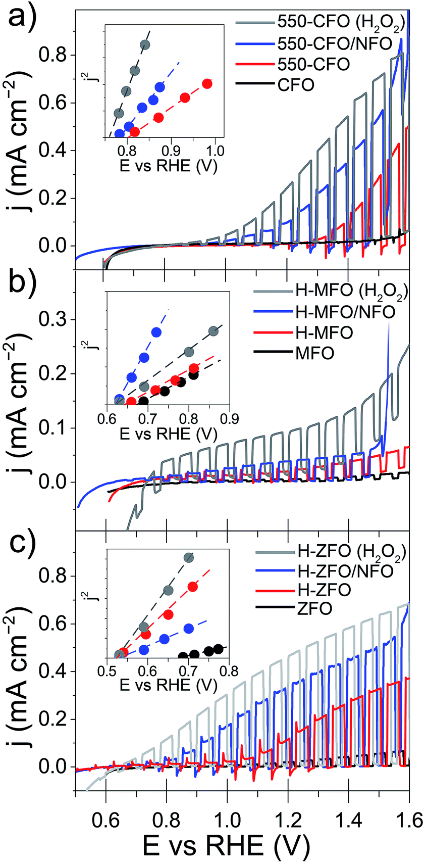 | ||
| Fig. 5 Linear sweep voltammograms under chopped-light illumination for CFO (a), MFO (b) and ZFO (c) as a function of the treatment (annealing or NFO-coating) and electrolyte. Corresponding Butler plot is included as an inset in each case. The electrolyte employed was typically 1 M NaOH except for those measurements displayed in grey termed as “(H2O2)” which were obtained in 1 M NaOH + 0.5 M H2O2. All the experiments were obtained under an irradiance of 1 sun (AM 1.5G) using a scan rate of 10 mV s−1. | ||
All the samples, even after the annealing post-treatment, display a very poor photocurrent onset voltage compared to the expected flat-band potentials (vide infra). This can be due to strong surface recombination and/or the sluggish kinetics for the water oxidation reaction on the oxide surface. The incorporation of NiFeOx (NFO) on the surface of oxide photoanodes has been reported to effectively promote water photooxidation,68 albeit its role as electrocatalyst or passivating agent in these systems is still a matter of active discussion.69,70 In all cases NFO-coated spinel ferrites (blue lines in Fig. 5) show dark current onsets at about 1.5–1.6 V vs. RHE related to the electrocatalytic water oxidation by NFO.71,72 In addition they display an enhanced photocurrent performance compared to the bare samples, especially in the case of CFO and ZFO, with a significant improvement in photocurrent and turn-on voltage. It is worth mentioning that Lee and co-workers previously described ZFO with a Co–Pi electrocatalyst overlayer, but reported lower performance with the added catalyst,28 which suggests that the interface between the spinel ferrite and catalyst is an important parameter. Nevertheless, all of the photocurrent values obtained here are far below the maximum photocurrent attainable based on the band gap of the materials. Indeed, considering only the absorption of solar photons with energy above the direct optical absorption transition energy, maximum photocurrent values of 8.5 mA cm−2 (CFO), 4.7 mA cm−2 (MFO) and 5.2 mA cm−2 (ZFO) under standard illumination conditions could be expected.
In addition to the low photocurrent the onset voltage is significantly delayed with respect the flat band potential (Efb), as estimated from using the j2 Butler method (inset Fig. 5).73 Without catalyst the estimated Efb is 0.8, 0.65 and 0.5 V vs. RHE for CFO, MFO and ZFO, respectively. It is worth noting that Efb remains virtually unchanged upon the different treatments (except in the case of bare ZFO probably because of the poor film conductivity), which indicates that the position of the band edges is not altered. In addition, we note that our efforts to extract Efb from Mott–Schottky plots were unsuccessful, suggesting the assumptions of the traditional Mott–Schottky model74 are not applicable to these nanostructured thin films. Overall, the poor performance of the spinel ferrite photoelectrodes points to a strong recombination within the bulk or in the surface of the materials.
In an attempt to decouple the effects of bulk and surface recombination on the observed PEC response, the optimized samples (without NFO) were tested in an electrolyte containing a hole scavenger (H2O2)75 to estimate the photocurrent in absence of surface recombination. The response of the ferrospinels in the presence of H2O2 is shown in Fig. 5 (grey curves) and in all the cases, a marked increase of the photocurrent was observed together with the disappearance of transient spikes (see Fig. S4, ESI†), which are related to hole accumulation at the SCLJ. Despite the improvement in photocurrent the values are still below the maximum expected values previously mentioned, clearly indicating severe bulk limitations on these materials.
For the sake of comparison with previous reports on metal oxide photoanodes, the charge separation efficiency in the bulk (ηbulk) and the charge transfer efficiency at the SCLJ (ηsurface) extracted from comparing the measurement under sacrificial and non-sacrificial conditions75 were estimated and are shown in Fig. 6. In all the cases, ηsurface increases with increasing applied positive bias, in agreement with the mitigation of surface recombination when increasing band bending. Interestingly, the deposition of NFO causes a significant improvement in the charge separation reaching values of around 60–80% at 1.4 V vs. RHE, similar to other photoanodes.28,29,75 This suggests that the NFO either effectively reduces the energetic barrier for water oxidation (catalytic effect) or suppresses the density of surface states at the interface (passivating effect). On the other hand, albeit ηbulk ameliorates for larger applied potentials in concert with the widening of the space charge depletion layer, the values are markedly low – remaining below 15% in all cases—and severely poor in the case of MFO (<2% even at high anodic bias).
 | ||
| Fig. 6 Yield of charge transfer (ηsurface, left axis and full markers) and of charge separation (ηbulk, right axis and empty markers) determined for CFO (a), MFO (b) and ZFO (c) as a function of the treatment. | ||
Overall, these results quantitatively reflect that bulk recombination poses an important bottleneck for the performance. We speculate that the low carrier mobility of the spinel ferrites, reported to be on the order of 10−8 cm2 V−1 s−1 for high-temperature annealed polycrystalline samples76 (compared to the typically reported values of 10−1 cm2 V−1 s−1 for other oxide photoanodes77–80), and possibly short diffusion lengths on the order of a few nanometers (similar to Fe2O3 (ref. 81)) are likely the key parameters limiting the bulk performance. It is important to bear in mind that the morphology of the films can also dictate the bulk response.82 In fact, the difference in ηbulk could be originated at least partially from different film morphology. A higher ηbulk is found in the ZFO thin-film that displays a well-ordered nanorod array facilitating the extraction of the holes and providing a continuous pathway to reach the conductive substrate. While the nanoparticulate structure of the CFO does display a favorably high SCLJ interfacial area to facilitate the charge separation, a potentially higher density of grain boundaries would limit the transport of the majority carriers towards the collector. Finally, the poor ηbulk obtained for the MFO could potentially be ascribed to the high-density of grain boundaries generated in the intertwined network of nanowires that constitute the thin-film in that case.
To verify the measured magnitude of the photocurrent density under 1 sun conditions and to evaluate the relative conversion efficiency at different wavelengths of absorbed photons, the incident photon-to-current efficiency (IPCE) was measured for each spinel (Fig. 7). In all the cases, the photocurrents predicted for 1 sun illumination by integrating the IPCE and standard solar spectrum matched quite well with the photocurrent measured by the LSVs (at comparable applied bias) indicating that the degree of recombination is not markedly affected by the lower light intensity of the IPCE measurement. Careful comparison of the UV-Vis absorption spectra with the IPCE revealed a severe weakening of the photocurrent response at long wavelengths. As a result, the onset of the IPCE appears to be blue-shifted with respect to the light absorption, about 50 nm, 100 nm and 250 nm for MFO, ZFO and CFO, respectively. Concretely, the onset of the photocurrent response matches quite well with the estimated direct band gap energy in each case, whereas the indirect band gap appears to be inactive, which is in agreement with previous reports on Fe2O3 (ref. 83) and CaFe2O4,30 and attributed to small polaron formation and the resulting rapid recombination of photogenerated carriers.84
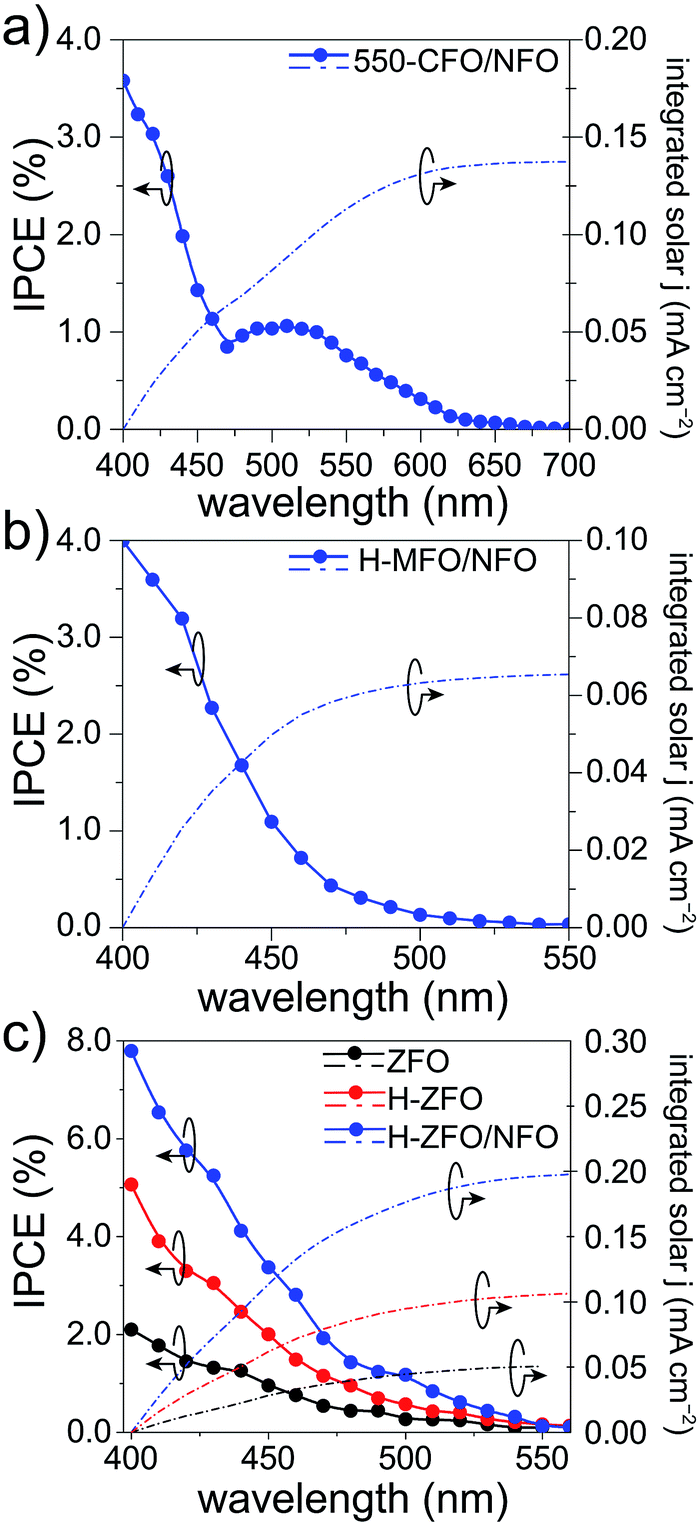 | ||
| Fig. 7 IPCE spectra of 550-CFO/NFO recorded at 1.23 V vs. RHE (a), of H-MFO/NFO at 1.4 V vs. RHE (b) and of ZFO at 1.1 V vs. RHE (left axis), including the integrated photocurrent (right axis) considering AM 1.5G irradiance. Measurements were done using 1 M NaOH as electrolyte. | ||
Taken together, the basic PEC characterization of the spinel ferrites reveals a poor n-type response of the native electrodes that can be significantly enhanced by implementing different post-treatments aimed at addressing intrinsic issues of the as-prepared films, viz. poor crystallinity, low mobility and catalytic activity. Notwithstanding the improvement, the photocurrent values are far from those expected according to the light absorption. The presence of severe surface and especially bulk problems are evident. The analysis of the photocurrent onset suggests the presence of a Fermi level pinning likely caused by a large density of surface states. Likewise, the very low ηbulk revealed that the bulk recombination probably arising from a very low mobility and diffusion length of the carriers or a high density of bulk defects is ultimately governing the response. We note that the incorporation of NFO results in a marked improvement of the PEC performance, especially on the onset voltage. Two different phenomena could explain this result, either an improvement on the kinetics of charge transfer (catalytic effect) or the mitigation of the Fermi level pinning (passivation effect). Next, open circuit potential and rapid cyclic voltammetry measurements are discussed to shed some light into the role of the NFO layer.
Fig. 8 shows the steady-state open circuit potential (EOC, also referred to as OCP) values obtained in dark and under illumination for the spinel ferrites as a function of the different treatments. In the absence of illumination and if the electrolyte is saturated in O2 prior to the measurement, the steady-state EOC in the dark (EOC,dark) should ideally equal the redox potential of the OER reaction, i.e. 1.23 V vs. RHE.68,69 This was not found to occur for any condition tested suggesting an equilibration rather with surface states, which causes the voltage drop to occur mainly across the Helmholtz layer instead of within the space-charge region. Interestingly, the degree of pinning appears to be reduced with subsequent thermal treatments, i.e. the EOC,dark is closer to 1.23 V vs. RHE. We hypothesize that in the case of CFO, this amelioration could be linked to surface reconstruction occurring under the long annealing treatment, which, in turn, would explain the marked changes in the XPS O 1s signal. However, and contrary to recent reports on Fe2O3 and TiO2 coated with NFO,68,87 no further improvement of the EOC,dark is observed upon NFO deposition. This result suggests the NFO is unable to completely suppress the surface states of the ferrites, therefore casting doubt on its role as passivating agent. Reasonably we can then conclude that the nature of the surface states on the spinel ferrites are different from surface-adsorbed species (such as H2O, OH−, or H+), which have been shown to be passivated by NFO coating,87 and could potentially be related to the iron deficiency located ubiquitously close to the surface. Moreover, the fact that all the spinels reach approximately the same EOC,dark (ca. 0.85–0.9 V) in the dark, suggests a common origin for these mid-gap trapping states pinning the Fermi level. For example, in the case of H-ZFO the density of surface states is located at around 0.88 V vs. RHE, i.e. approximately 1.8 V above the valence band edge provided that the band edge positions are pinned.‡ We note as well that the dark EOC when H2O2 is incorporated in the solution is around 0.95 V vs. RHE which is far from the expected O2/H2O2 redox couple in the solution (approximately 0.70 V vs. RHE88). This is not unexpected since a noticeable delay between the Efb and the turn-on voltage was observed even in the presence of H2O2.
 | ||
| Fig. 8 Steady-state OCP values of CFO, MFO and ZFO with respect to the different treatments (annealing, presence of H2O2 and NFO-coating) both in dark (black squares) and under illumination (red circles—1 sun—and blue triangles—14 suns—). The error bars were obtained by averaging the EOC over three different samples prepared in the same way. | ||
Under illumination the photovoltage (Vph = EOC,dark − EOC,light) generated by the photoanodes increases after the annealing post-treatment due to a simultaneous increase of the EOC,dark and decrease of EOC,light. In accordance with previous discussion, a more positive EOC,dark arises from the partial reduction of the Fermi level pinning due to the electrode generating a larger band bending at equilibrium leading to a higher Vph when the bands are flattened under illumination. A more negative EOC,light points to an increased accumulation of majority carriers (electrons) in the film under illumination. This phenomenon could be accounted for by the improvement in mobility and the reduction of surface/bulk recombination triggered by the annealing post-treatments. Intriguingly, the deposition of NFO did not cause a noticeable change in Vph. This further reinforces the hypothesis that the NFO does not affect the states of the ferrite associated with the Fermi level pinning. However, there exists a modest decrease in EOC,light that could stem from the ability of the ferrites to transfer holes to the NFO, which, in turn, would reduce the recombination and shift EOC,light to more negative values.85 As expected, experiments performed in the presence of H2O2 delivered similar values of Vph. It is well-known that given that the Fermi level pinning governs the EOC values the Vph remains unaltered regardless the redox couple present in the electrolyte.89
It is worth mentioning that EOC,light at sufficiently high illumination intensity can also be employed to estimate Efb,90 since it corresponds to the situation where the bands are flattened by action of the built-in field created by the photogenerated carriers within the semiconductor. In our case 14 suns illumination is shown to saturate the Vph (Fig. S5, ESI†) suggesting that Efb is equal to EOC,light in this case. We note that these estimated values of Efb are very close to those obtained from the Butler j2 method,73 especially for the treated samples. Overall, the study of the EOC measurement provides compelling evidence that the energetics of the photoanode remains unaltered after the incorporation of the NFO, which clearly discards its effect as a passivating agent but reinforces the idea that it indeed works as an electrocatalyst mediating in the water oxidation reaction in this system. We next attempt to gain more insights into the location of the density of surface states and its effect on the water oxidation reaction for the two best working materials (ZFO and CFO).
The validity of the RSV technique was first established with H-ZFO and 550-CFO electrodes by scanning at 200, 400, 600 and 800 mV s−1 (Fig. S6 and S7, ESI†). In all cases, distinct cathodic features in the first RSV scan disappear in a second scan clearly showing the expected behavior of discharge of charges accumulated in discrete surface states. Fig. 9 summarizes the RSV technique results by comparing the standard LSV curves under intermittent illumination and the extracted capacitance corresponding to the baseline-corrected first rapid voltammetry scan at 200 mV s−1 for H-ZFO and 550-CFO (see ESI for details†). For the bare H-ZFO (Fig. 9a) a broad capacitance peak is observed centered at a potential of ca. 1.0 V vs. RHE (i.e. the water photooxidation onset potential). Previous interpretation of RSV data has attributed a capacitance appearing close to the photocurrent onset potential to water oxidation intermediates rather than actual surface states that cause Fermi level pinning.61,91 In our case, the compelling evidence of Fermi level pinning occurring at a similar potential (EOC,dark is pinned at 0.9 V vs. RHE for H-ZFO), together with the fact that the capacitance recorded by RSV barely changes with the scan rate (Fig. S6†) (i.e. the accumulated holes do not decrease rapidly over time), suggests that this feature corresponds to surface states inherent to the electrode rather than intermediates.91 However, we cannot completely discount an overlap with water oxidation intermediates which would potentially be found within the same potential range. Interestingly, RSV carried out in the presence of H2O2 does not reveal any discharge band (Fig. S8, ESI†). We hypothesize that surface-trapped holes responsible for the pinning could be removed to a great extent by H2O2 given its more negative redox potential, leaving an undetectable signal in RSV but still influencing the EOC,dark, since intermediates would decay prior detection by RSV given the faster kinetics of H2O2 oxidation compared to H2O. In contrast to the H-ZFO sample, RSV results using a bare 550-CFO electrode (Fig. 9b) clearly show two cathodic bands. The first one centered at around 0.8 V vs. RHE is close to EOC,dark, whereas the second band, appearing at 1.4 V vs. RHE, is near the onset voltage. We attribute the first band to surface traps inherent to the electrode that govern the Fermi level pinning (as this is close to EOC,dark and does not change with scan rate) whereas the second band that appears to decrease over time could be linked to intermediate states involved in the water oxidation (Fig. S7†). This observation reinforces the idea that surface trapping states and the water oxidation intermediates could overlap for the H-ZFO electrode (Fig. 9a).
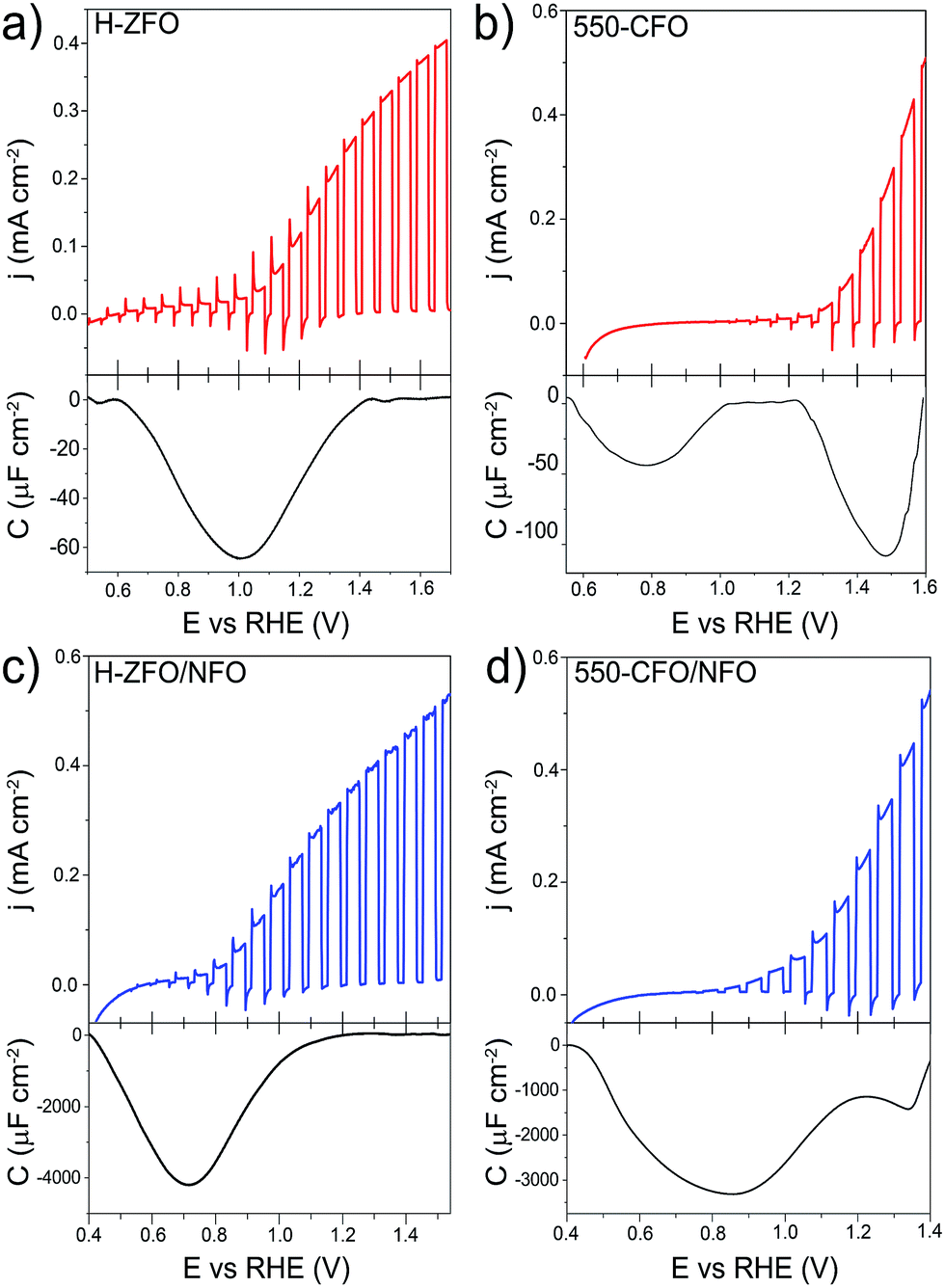 | ||
| Fig. 9 Linear sweep voltammograms under chopped-light illumination (simulated 1 sun) for bare H-ZFO (a, top) and 550-CFO (b, top) and the corresponding baseline-corrected capacitance vs. potential curves obtained from the RSV performed at 200 mV s−1 in dark conditions (a and b, bottom). Linear sweep voltammograms under chopped-illumination for the NFO-coated ZFO (c, top) and CFO (d, top) with the corresponding RSV curves obtained at 50 mV s−1 in dark conditions (c and d, bottom). See complete RSV experiments as a function of the scan rate and deconvolution in Fig. S6, S7 and S10–S12.† | ||
For both H-ZFO and 550-CFO electrodes, the deposition of NFO provokes a remarkable increase of the capacitance (Fig. 9c and d respectively), reasonably due to the accumulation of holes in this porous overlayer (intermediates). This provides further evidence that the NFO is actively accepting photogenerated holes, and therefore, actively participating in the water oxidation reaction as a catalyst rather than merely inhibiting surface recombination. The bands are detected near the onset of photocurrent in both cases. This is not unexpected since the charging–discharging of the catalyst is known to be shifted by the photovoltage generated within the semiconductor, therefore, being perceived at the onset of photocurrent although its real location would be at around 1.3–1.4 V vs. RHE (Fig. S9, ESI†). However, the marked differences between the RSV fingerprints obtained for NFO-coated CFO and ZFO are rather surprising, especially when considering that the same kind of accumulated holes (those in the NFO) are expected to be mainly tracked regardless the underlying spinel. In the case of ZFO we obtained a single band that shifts to more negative potentials with the scan rate (Fig. S10, ESI†) similar to the two major Gaussian bands deconvolved in the RSV signals of the CFO (Fig. S11 and S12, ESI†). These bands were attributed to intermediates within the NFO in contact with the semiconductor, where the slow kinetics for charge transfer from the back contact through the semiconductor to the NFO would account for the shift with scan rate. In contrast, the slight shoulder located at around 1.3 V vs. RHE in CFO does not shift with scan rate and resembles the water oxidation intermediate peak found in the bare film. This supports the idea that catalysis can simultaneously occur on the bare and catalyst-coated surface of the semiconductor photoelectrode.
It is worth remarking that although the RSV technique is effective at qualitatively evaluating charge accumulation at the electrode/electrolyte interface, quantitatively determining the energetic position of these charges is complicated by aspects of transport through the semiconducting layer as well as the kinetics for the charge transfer processes. In our experiments where the RSV is performed in the absence of illumination and under the reverse bias regime for n-type materials, the conduction of charges through the n-type semiconductor likely depends strongly on the applied potential (built-in electric field at the SCLJ) and the conductivity of the material (which is strongly affected by extrinsic defects). In the case of the RSV of NFO-treated films (Fig. 9c and d) a delay in the detection of the accumulated charges is apparent as the peak for the intermediate species is centered at a potential more negative than the expected 1.3–1.5 V vs. RHE expected for an intermediate for oxygen evolution. This apparent shift likely originates from the resistance of charge conduction through the semiconductor under such a reverse bias. The resistance reasonably decreases when scanning towards more negative potentials, allowing the necessary current to flow through the semiconductor. This phenomenon is also evident from the LSV curves (Fig. 9a and c) where the transient cathodic spikes—related to the current injected from the external circuit to the semiconductor to recombine with surface holes—only exist within the potential range where the capacitive band is recorded. The gradual disappearance of transient spikes at more positive applied potentials is usually linked to the improved kinetics for the oxidation reaction (absence of surface holes), but we cannot rule out the possibility that the barrier imposed by the high reverse bias would prevent a rapid back electron recombination from the external circuit when the light is turned off. Indeed, the absence of transient cathodic spike accompanied by a slow decay of surface holes was recently reported by Durrant and co-workers when studying the kinetics of water oxidation in Fe2O3.92 Following this line of thought, we believe that the striking differences in the RSV response of NFO-coated ZFO and CFO could emerge not from a different nature or location of the reaction intermediates, which are presumably the same, but from the intrinsic properties (viz. conductivity, energetic distribution of defects, leakage current) of the semiconductor which could ultimately govern the detection of the surface-charges. Likewise, the identification of surface-trapped holes in the bare films could be equally influenced by the bulk properties of the semiconductor accounting for shifts in the energetic location of the surface charges. This discussion does not attempt to shed doubts on previous studies of RSV reported for ALD-deposited Fe2O3,61,91 which demonstrated high reproducibility likely due to a high doping density and thinness of the films (reducing charge transport resistance), but emphasizes the limitations of this analysis.
We note that we also conducted electrochemical impedance spectroscopy measurements to gain insight into the electrical properties of the electrode–electrolyte interface and into the density and location of the surface states. However, no noticeable changes in the resistance or capacitance across the interface as a function of the potential were detected. We assume that the high resistance of the films and the high density of surface states ultimately limit these measurements as previously noted.
Stability assessment and faradaic efficiency for oxygen evolution reaction
Long-term stability of photoelectrodes is one of the key limitations for the realization of feasible tandem cell devices. To evaluate the robustness of the spinel ferrites under operating conditions the photocurrent under constant applied bias (1.23 V vs. RHE) was recorded under chopped-light illumination (1 sun) for 60 min. As expected, no signal of degradation was observed in any of the cases during the test up to 24 hours, i.e. the photocurrent remains constant and equal to the value recorded in the J–V curve (Fig. S13 and S14 ESI†).Throughout this work we assumed that the photocurrent produced by the electrodes is mostly related to the water oxidation reaction. However, for some systems a significant part of the photocurrent arises from photocorrosion processes or even other water oxidation routes (e.g. generation of H2O2 or ˙OH). To ascertain the faradaic efficiency for molecular oxygen evolution, the amount of O2 produced by the NFO-coated spinels was tracked with a gas chromatograph while the electrode was illuminated under applied bias (Fig. S15, ESI†). The results demonstrated a faradaic efficiency of 99 ± 1% (ZFO), 97 ± 2% (CFO) and 97 ± 1% (MFO). Overall, the longevity and chemical robustness of these materials together with the selective production of O2 in combination with NFO confirm their attractiveness as photoanodes for tandem cells, provided that the performance is improved.
Conclusions
In this work we have reported a comprehensive study of the PEC properties of a series of thin-film spinel ferrites electrodes (CFO, MFO and ZFO), with the aim of gaining insights into their intrinsic limitations and prospective future implementation as active photoelectrodes in PEC cells. Analysis of the J–V curves under illumination revealed a very modest performance that could be significantly improved by combining post-annealing treatments with the deposition of NFO. Notwithstanding the improvement, studies performed with H2O2 as sacrificial hole acceptor clearly identified the bulk recombination losses (ηbulk < 10%) as a main limiting factor in the performance, although the surface recombination (ηsurface < 80%) also plays a crucial role in limiting the performance. Additional measurements of the steady-state OCP demonstrated that all the ferrites tested, even upon coating with NFO, exhibit a strong Fermi level pinning at around 0.9 V vs. RHE limiting the attainable photovoltage. This result shows that the enhancement in performance induced by the NFO coating comes from improved water oxidation kinetics rather than the mitigation of surface states. Further studies on the surface characteristics of the bare films by RSV revealed the accumulation of holes at potentials where the pinning was detected to occur by OCP, whereas the examination of NFO-coated films provided clear evidence of catalyst charging supporting the active role of this layer as catalyst for water oxidation. Finally, the robustness of the ferrites under operation was certified without noticeable changes in the performance after hours of testing, displaying faradaic efficiencies for oxygen production above 97%.Overall these results present a general view on the benefits and inherent drawbacks of the spinel ferrites as photoanodes for water oxidation. The robustness of the electrode is clearly an advantage for the design of long-term operating cells as long as the low saturation photocurrents and turn-on voltages are addressed. New synthetic routes affording better control on the morphology, reduction of grain boundaries and enhanced conductivity would significantly reduce the bulk recombination losses responsible for the limited photocurrents. Indeed, tight control on the degree of Sn-doping and the concentration of oxygen vacancies has shown to ameliorate remarkably the performance of hematite photoanodes.93,94 An in-depth characterization of the surface states responsible for the Fermi level pinning would provide a solid platform to engineer the surface and deliver reasonable photovoltages. For instance, careful selection of electrocatalytic overlayers could not only reduce the overpotential for water oxidation but concomitantly mitigate the surface recombination and modulate the photovoltage generated at the SCLJ.57,95 Likewise, a thorough characterization of the charge carrier mobility and diffusion length in the spinel ferrites could also shed some light onto the optimum architecture for these thin-film electrodes. Further efforts in this vein are underway in our laboratory.
Experimental methods
Fabrication of spinel ferrites thin-film electrodes
The spinel ferrites were prepared by modifying the two-step solution-based route reported by Kim et al.28 for the synthesis of CFO, MFO and ZFO. First, a layer of β-FeOOH was grown on F: SnO2 (FTO) substrate (Solaronix TCO10-10) by following the procedure reported by Hagfeldt and co-workers.59 The electrodes were positioned standing (with the conductive side facing the solution) in a 0.15 M FeCl3·6H2O (99%, Acros) and 1 M NaNO3 (99%, Acros) aqueous solution (note that the pH was around 1.3 without requiring further adjustment) in a tightly capped glass bottle. Subsequently, these bottles were introduced in an oven pre-heated at 100 °C for 5 hours. The resulting FeOOH-coated FTO was washed thoroughly with ultrapure water and dried with compressed air. Second, the FTO/FeOOH electrodes were placed in a hot-plate at 100 °C and coated (drop-casting) with a 0.1 M metal nitrate aqueous solution, viz. Cu(NO3)2·3H2O (99%, Sigma-Aldrich), Mg(NO3)2·6H2O (99%, Sigma-Aldrich) and Zn(NO3)2·6H2O (98%, abcr) for CFO, MFO and ZFO, respectively. Finally, the spinel ferrite formation was carried out by introducing the metal nitrate-coated FeOOH samples into a tubular oven (MTI OTF-1200X) pre-heated at 800 °C for 30 min and removing them from the oven right after the annealing to allow them to cool-down naturally. The resulting samples are coated by a thick crust of the corresponding metal oxide (CuO, MgO or ZnO) on the surface, that can be etched away chemically by soaking the samples in a 5 M NaOH (ZFO) or 7 M HNO3 (CFO, MFO) aqueous solution for 4 hours to ensure complete dissolution.Annealing post-treatments
Two different annealing post-treatments were performed. CFO were annealed at 550 °C for 5 hours in air (labelled as 550-CFO). MFO and ZFO were annealed at 200 °C for 1 h under hydrogen (H-MFO and H-ZFO).NiFeOx deposition
All the samples were coated with NiFeOx (NFO), by following the procedure reported by Smith et al. A precursor solution containing iron(III) 2-ethylhexanoate (50% w/w in mineral spirits, Strem Chemicals) and nickel(II) 2-ethylhexanoate (78% w/w in 2-ethylhexanoic acid, Strem Chemicals) were dissolved in hexane so as to achieve a 1:1 Fe:Ni molar ratio and a total concentration of 15% w/w for the metal complexes in solution.72 This solution was diluted ten-times with hexane and approximately 10 μL cm−2 were drop-casted onto the active surface area of electrode. The electrode was allowed to dry in air followed by UV irradiation (Atlantic Ultraviolet G18T5VH/U lamp) for 10 min. Finally, the electrode was annealed at 100 °C for 1 hour.68
Photoelectrochemical characterization
All the experiments were carried out employing a potentiostat (BioLogic SP-300) and a Capuccino-type PEC cell, where a Ag/AgCl KCl (sat.) electrode and a Pt wire where used as reference and counter electrode, respectively, and the active geometric area of the working electrode was 0.238 cm2. Two different electrolytes were employed: 1 M NaOH or 1 M NaOH + 0.5 M H2O2, purging with O2 the solution when indicated in the corresponding figure caption. Chopped-light linear sweep voltammograms and open circuit potential (OCP) measurements under illumination were performed using a 450 W Muller Elektronik Xenon-arc lamp coupled with a KG-1 filter (Schott) calibrated to provide 1 sun (AM 1.5G, 100 mW cm−2). Light intensities over 1 sun were achieved by including converging lenses on the light path and using a calibrated Si-diode to determine the irradiance. The yield of charge transfer was calculated by using ηsurface = jH2O/jH2O2 whereas the yield of charge separation was determined with ηbulk = jH2O2/jabs, where jH2O and jH2O2 correspond to the photocurrent for water and H2O2 oxidation, respectively, whereas jabs is the maximum photocurrent attainable considering that all the light absorbed by the thin film is turned into photogenerated carriers with 100% collection efficiency. Note for the OCP measurements the electrolyte was saturated in oxygen (by bubbling O2 in the solution during the experiment) to define the H2O/O2 and H2O2/O2 redox couples. All the OCP values shown were obtained upon reaching steady-state (in the absence of H2O2 longer times where required for equilibration in dark – approx. 1 h – and under illumination – approx. 10 min). Incident photon to current efficiency (IPCE) were performed using a Tunable PowerArc illuminator (Optical Building Block Corporation) as light source coupled to a monochromator and determining the photon flux at each wavelength with a S120VC Photodiode Power sensor (Thorlabs). Rapid-scan cyclic voltammograms were obtained through a two-step process with a minimum delay in-between. First, the electrodes were held at a potential indicated in the corresponding figure caption under constant-illumination (chronoamperometry) for 60 seconds, followed by the interruption of the illumination and the measurement of the cyclic voltammogram scanning in the negative direction from the potential held during the chronoamperometry. The capacitance was calculated by dividing the current associated to the accumulated charges by the scan rate in each case. Two different electrolytes were employed, viz. 1 M NaOH and 1 M NaOH + 0.5 M H2O2 aqueous solutions. In all the cases the electrodes were illuminated from the back-side, and for the sake of comparison with other reports, the potential has been referred to the reversible hydrogen electrode (RHE) potential.Materials characterization
UV-Vis absorption spectra of the thin-film were recorded with a UV-Vis-NIR UV-3600 (Shimadzu) spectrophotometer. The thickness of the as-prepared FTO/FeOOH thin-films was obtained by using a Dektak XT (Bruker) profilometer. TEM images were obtained using a FEI Tecnai Osiris microscope equipped with an energy-dispersive X-ray (EDX) system. SEM images were collected with a Zeiss Merlin microscope. XRD were recorded with an Empyrean (PANalytical) diffractometer. Raman spectra were measured with an Xplora Plus Raman microscope (Horiba Scientific) using an excitation line of 532.19 nm provided by a diode laser. XPS surveys and narrow-scan spectra were acquired using a KRATOS AXIS ULTRA spectrometer (Al Kα source, 600 × 750 μm spot size). The depth profile measurements were obtained by etching the sample with Ar+ sputtering before the XPS acquisition at each depth.Conflicts of interest
There are no conflicts to declare.Acknowledgements
The authors thank the Swiss Competence Centre for Energy Research (SCCER Heat and Electricity Storage, contract #KTI.2014.0113) and the Swiss National Science Foundation (project no. 200021_149251). N. G. is grateful to the Swiss National Foundation for the award of an Ambizione Energy grant (PZENP2_166871).Notes and references
- A. J. Bard, J. Phys. Chem., 1982, 86, 172–177 CrossRef CAS.
- M. G. Walter, E. L. Warren, J. R. McKone, S. W. Boettcher, Q. Mi, E. A. Santori and N. S. Lewis, Chem. Rev., 2010, 110, 6446–6473 CrossRef CAS PubMed.
- M. Grätzel, Nature, 2001, 414, 338–344 CrossRef PubMed.
- M. S. Prévot and K. Sivula, J. Phys. Chem. C, 2013, 117, 17879–17893 Search PubMed.
- O. Khaselev and J. A. Turner, Science, 1998, 280, 425–427 CrossRef CAS PubMed.
- M. S. Prévot, N. Guijarro and K. Sivula, ChemSusChem, 2015, 8, 1359–1367 CrossRef PubMed.
- X. Yu, M. S. Prévot, N. Guijarro and K. Sivula, Nat. Commun., 2015, 6, 7596 CrossRef PubMed.
- N. Guijarro, M. S. Prévot, X. Yu, X. A. Jeanbourquin, P. Bornoz, W. Bourée, M. Johnson, F. Le Formal and K. Sivula, Adv. Energy Mater., 2016, 6, 1501949 CrossRef.
- N. Guijarro, M. S. Prévot, M. Johnson, X. Yu, W. S. Bourée, X. A. Jeanbourquin, P. Bornoz, F. L. Formal and K. Sivula, J. Phys. D: Appl. Phys., 2017, 50, 044003 CrossRef.
- M. Neumann-Spallart and K. Kalyanasundaram, J. Phys. Chem., 1982, 86, 2681–2690 CrossRef CAS.
- J. L. White, M. F. Baruch, J. E. Pander III, Y. Hu, I. C. Fortmeyer, J. E. Park, T. Zhang, K. Liao, J. Gu, Y. Yan, T. W. Shaw, E. Abelev and A. B. Bocarsly, Chem. Rev., 2015, 115, 12888–12935 CrossRef CAS PubMed.
- K. Sivula and R. van de Krol, Nat. Rev. Mater., 2016, 1, 16010 CrossRef.
- F. F. Abdi and S. P. Berglund, J. Phys. D: Appl. Phys., 2017, 50, 193002 CrossRef.
- R. Dillert, D. H. Taffa, M. Wark, T. Bredow and D. W. Bahnemann, APL Mater., 2015, 3, 104001 CrossRef.
- N. Helaili, G. Mitran, I. Popescu, K. Bachari, I.-C. Marcu and A. Boudjemaa, J. Electroanal. Chem., 2015, 742, 47–53 CrossRef CAS.
- A. Kezzim, N. Nasrallah, A. Abdi and M. Trari, Energy Convers. Manage., 2011, 52, 2800–2806 CrossRef CAS.
- W. Fan, M. Li, H. Bai, D. Xu, C. Chen, C. Li, Y. Ge and W. Shi, Langmuir, 2016, 32, 1629–1636 CrossRef CAS PubMed.
- R. Dom, A. S. Chary, R. Subasri, N. Y. Hebalkar and P. H. Borse, Int. J. Energy Res., 2015, 39, 1378–1390 CrossRef CAS.
- M. G. Ahmed, T. A. Kandiel, A. Y. Ahmed, I. Kretschmer, F. Rashwan and D. Bahnemann, J. Phys. Chem. C, 2015, 119, 5864–5871 CAS.
- Y. Guo, Y. Fu, Y. Liu and S. Shen, RSC Adv., 2014, 4, 36967–36972 RSC.
- K. J. McDonald and K.-S. Choi, Chem. Mater., 2011, 23, 4863–4869 CrossRef CAS.
- E. S. Kim, N. Nishimura, G. Magesh, J. Y. Kim, J.-W. Jang, H. Jun, J. Kubota, K. Domen and J. S. Lee, J. Am. Chem. Soc., 2013, 135, 5375–5383 CrossRef CAS PubMed.
- E. S. Kim, H. J. Kang, G. Magesh, J. Y. Kim, J.-W. Jang and J. S. Lee, ACS Appl. Mater. Interfaces, 2014, 6, 17762–17769 CAS.
- N. Helaïli, Y. Bessekhouad, K. Bachari and M. Trari, Mater. Chem. Phys., 2014, 148, 734–743 CrossRef.
- M. I. Díez-García, T. Lana-Villarreal and R. Gómez, ChemSusChem, 2016, 9, 1504–1512 CrossRef PubMed.
- A. A. Tahir and K. G. U. Wijayantha, J. Photochem. Photobiol., A, 2010, 216, 119–125 CrossRef CAS.
- A. G. Hufnagel, K. Peters, A. Müller, C. Scheu, D. Fattakhova-Rohlfing and T. Bein, Adv. Funct. Mater., 2016, 26, 4435–4443 CrossRef CAS.
- J. H. Kim, J. H. Kim, J.-W. Jang, J. Y. Kim, S. H. Choi, G. Magesh, J. Lee and J. S. Lee, Adv. Energy Mater., 2015, 5, 1401933 CrossRef.
- J. H. Kim, Y. J. Jang, J. H. Kim, J.-W. Jang, S. H. Choi and J. S. Lee, Nanoscale, 2015, 7, 19144–19151 RSC.
- S. Ida, K. Yamada, T. Matsunaga, H. Hagiwara, Y. Matsumoto and T. Ishihara, J. Am. Chem. Soc., 2010, 132, 17343–17345 CrossRef CAS PubMed.
- D. Carta, M. F. Casula, A. Falqui, D. Loche, G. Mountjoy, C. Sangregorio and A. Corrias, J. Phys. Chem. C, 2009, 113, 8606–8615 CAS.
- R. G. Kulkarni, B. S. Trivedi, H. H. Joshi and G. J. Baldha, J. Magn. Magn. Mater., 1996, 159, 375–380 CrossRef CAS.
- Y. Tang, K. Shih, C. Liu and C. Liao, RSC Adv., 2016, 6, 28579–28585 RSC.
- W. Cheng, K. Tang, Y. Qi, J. Sheng and Z. Liu, J. Mater. Chem., 2010, 20, 1799–1805 RSC.
- M. D. P. Silva, F. C. Silva, F. S. M. Sinfrônio, A. R. Paschoal, E. N. Silva and C. W. A. Paschoal, J. Alloys Compd., 2014, 584, 573–580 CrossRef CAS.
- K. Verma, A. Kumar and D. Varshney, Curr. Appl. Phys., 2013, 13, 467–473 CrossRef.
- B. K. Chatterjee, K. Bhattacharjee, A. Dey, C. K. Ghosh and K. K. Chattopadhyay, Dalton Trans., 2014, 43, 7930–7944 RSC.
- Z. Wang, P. Lazor, S. K. Saxena and H. S. C. O'Neill, Mater. Res. Bull., 2002, 37, 1589–1602 CrossRef CAS.
- Z. Wang, D. Schiferl, Y. Zhao and H. S. C. O'Neill, J. Phys. Chem. Solids, 2003, 64, 2517–2523 CrossRef CAS.
- K. Murugappan, D. S. Silvester, D. Chaudhary and D. W. M. Arrigan, ChemElectroChem, 2014, 1, 1211–1218 CrossRef CAS.
- Y. Xu, J. Sherwood, Y. Qin, R. A. Holler and Y. Bao, Nanoscale, 2015, 7, 12641–12649 RSC.
- W. S. Bourée, M. S. Prévot, X. A. Jeanbourquin, N. Guijarro, M. Johnson, F. L. Formal and K. Sivula, Adv. Mater., 2016, 28, 9308–9312 CrossRef PubMed.
- M. A. Dar, Q. Ahsanulhaq, Y. S. Kim, J. M. Sohn, W. B. Kim and H. S. Shin, Appl. Surf. Sci., 2009, 255, 6279–6284 CrossRef CAS.
- R. Zhang, P.-G. Yin, N. Wang and L. Guo, Solid State Sci., 2009, 11, 865–869 CrossRef CAS.
- K. Ishikawa, N. Fujima and H. Komura, J. Appl. Phys., 1985, 57, 973–975 CrossRef CAS.
- N. S. Chaudhari, S. S. Warule, S. Muduli, B. B. Kale, S. Jouen, B. Lefez, B. Hannoyer and S. B. Ogale, Dalton Trans., 2011, 40, 8003–8011 RSC.
- W. Zhang, B. Quan, C. Lee, S.-K. Park, X. Li, E. Choi, G. Diao and Y. Piao, ACS Appl. Mater. Interfaces, 2015, 7, 2404–2414 CAS.
- B. T. V. Srinivas, V. S. Rawat, K. Konda and B. Sreedhar, Adv. Synth. Catal., 2014, 356, 805–817 CrossRef CAS.
- Handbook of X-ray photoelectron spectroscopy: a reference book of standard spectra for identification and interpretation of XPS data, ed. J. F. Moulder and J. Chastain, Perkin-Elmer Corporation, Eden Prairie, Minn, 1992 Search PubMed.
- Z. Yan, J. Gao, Y. Li, M. Zhang and M. Guo, RSC Adv., 2015, 5, 92778–92787 RSC.
- H.-L. Lu, S.-J. Ding and D. W. Zhang, Electrochem. Solid-State Lett., 2010, 13, G25–G28 CrossRef CAS.
- T. Yamashita and P. Hayes, Appl. Surf. Sci., 2008, 254, 2441–2449 CrossRef CAS.
- J. Liu, M. Zeng and R. Yu, Sci. Rep., 2016, 6, 25074 CrossRef CAS PubMed.
- K. Sivula, R. Zboril, F. Le Formal, R. Robert, A. Weidenkaff, J. Tucek, J. Frydrych and M. Grätzel, J. Am. Chem. Soc., 2010, 132, 7436–7444 CrossRef CAS PubMed.
- J. Frydrych, L. Machala, J. Tucek, K. Siskova, J. Filip, J. Pechousek, K. Safarova, M. Vondracek, J. H. Seo, O. Schneeweiss, M. Grätzel, K. Sivula and R. Zboril, J. Mater. Chem., 2012, 22, 23232–23239 RSC.
- Z. Liu, K. Wang, L. Xiao, X. Chen, X. Ren, J. Lu and L. Zhuang, RSC Adv., 2014, 4, 37701–37704 RSC.
- T. W. Kim and K.-S. Choi, Science, 2014, 343, 990–994 CrossRef CAS PubMed.
- B. A. Pinaud, P. C. K. Vesborg and T. F. Jaramillo, J. Phys. Chem. C, 2012, 116, 15918–15924 CAS.
- L. Vayssieres, N. Beermann, S.-E. Lindquist and A. Hagfeldt, Chem. Mater., 2001, 13, 233–235 CrossRef CAS.
- J. Brillet, M. Grätzel and K. Sivula, Nano Lett., 2010, 10, 4155–4160 CrossRef CAS PubMed.
- O. Zandi and T. W. Hamann, J. Phys. Chem. Lett., 2014, 5, 1522–1526 CrossRef CAS PubMed.
- X. Zhao, J. Feng, S. Chen, Y. Huang, T. C. Sum and Z. Chen, Phys. Chem. Chem. Phys., 2017, 19, 1074–1082 RSC.
- M. Rioult, D. Stanescu, E. Fonda, A. Barbier and H. Magnan, J. Phys. Chem. C, 2016, 120, 7482–7490 CAS.
- J.-W. Jang, D. Friedrich, S. Müller, M. Lamers, H. Hempel, S. Lardhi, Z. Cao, M. Harb, L. Cavallo, R. Heller, R. Eichberger, R. van de Krol and F. F. Abdi, Adv. Energy Mater., 2017, 1701536 CrossRef.
- J. K. Cooper, S. B. Scott, Y. Ling, J. Yang, S. Hao, Y. Li, F. M. Toma, M. Stutzmann, K. V. Lakshmi and I. D. Sharp, Chem. Mater., 2016, 28, 5761–5771 CrossRef CAS.
- D. A. Wheeler, G. Wang, Y. Ling, Y. Li and J. Z. Zhang, Energy Environ. Sci., 2012, 5, 6682–6702 CAS.
- M. Büchler, P. Schmuki, H. Böhni, T. Stenberg and T. Mäntylä, J. Electrochem. Soc., 1998, 145, 378–385 CrossRef.
- J.-W. Jang, C. Du, Y. Ye, Y. Lin, X. Yao, J. Thorne, E. Liu, G. McMahon, J. Zhu, A. Javey, J. Guo and D. Wang, Nat. Commun., 2015, 6, 7447 CrossRef PubMed.
- C. Du, X. Yang, M. T. Mayer, H. Hoyt, J. Xie, G. McMahon, G. Bischoping and D. Wang, Angew. Chem., Int. Ed., 2013, 52, 12692–12695 CrossRef CAS PubMed.
- J. E. Thorne, J.-W. Jang, E. Y. Liu and D. Wang, Chem. Sci., 2016, 7, 3347–3354 RSC.
- F. L. Formal, N. Guijarro, W. S. Bourée, A. Gopakumar, M. S. Prévot, A. Daubry, L. Lombardo, C. Sornay, J. Voit, A. Magrez, P. J. Dyson and K. Sivula, Energy Environ. Sci., 2016, 9, 3448–3455 Search PubMed.
- R. D. L. Smith, M. S. Prévot, R. D. Fagan, Z. Zhang, P. A. Sedach, M. K. J. Siu, S. Trudel and C. P. Berlinguette, Science, 2013, 340, 60–63 CrossRef CAS PubMed.
- M. A. Butler, J. Appl. Phys., 1977, 48, 1914–1920 CrossRef CAS.
- J. O. 'M. Bockris and S. U. M. Khan, in Surface Electrochemistry. A Molecular Level Approach, Springer, 1993 Search PubMed.
- H. Dotan, K. Sivula, M. Grätzel, A. Rothschild and S. C. Warren, Energy Environ. Sci., 2011, 4, 958–964 CAS.
- D. Ravinder, J. Alloys Compd., 1999, 291, 208–214 CrossRef CAS.
- T. Bak, M. K. Nowotny, L. R. Sheppard and J. Nowotny, J. Phys. Chem. C, 2008, 112, 12981–12987 CAS.
- F. F. Abdi, T. J. Savenije, M. M. May, B. Dam and R. van de Krol, J. Phys. Chem. Lett., 2013, 4, 2752–2757 CrossRef CAS.
- A. J. E. Rettie, H. C. Lee, L. G. Marshall, J.-F. Lin, C. Capan, J. Lindemuth, J. S. McCloy, J. Zhou, A. J. Bard and C. B. Mullins, J. Am. Chem. Soc., 2013, 135, 11389–11396 CrossRef CAS PubMed.
- S. S. Shinde, R. A. Bansode, C. H. Bhosale and K. Y. Rajpure, J. Semicond., 2011, 32, 013001 CrossRef.
- U. Bjoerksten, J. Moser and M. Graetzel, Chem. Mater., 1994, 6, 858–863 CrossRef CAS.
- F. E. Osterloh, Chem. Soc. Rev., 2013, 42, 2294–2320 RSC.
- J. Y. Kim, G. Magesh, D. H. Youn, J.-W. Jang, J. Kubota, K. Domen and J. S. Lee, Sci. Rep., 2013, 3, 2681 CrossRef PubMed.
- Y. Matsumoto, J. Solid State Chem., 1996, 126, 227–234 CrossRef CAS.
- J. W. Moir, E. V. Sackville, U. Hintermair and G. A. Ozin, J. Phys. Chem. C, 2016, 120, 12999–13012 CAS.
- X. Yang, C. Du, R. Liu, J. Xie and D. Wang, J. Catal., 2013, 304, 86–91 CrossRef CAS.
- C. Du, M. Zhang, J.-W. Jang, Y. Liu, G.-Y. Liu and D. Wang, J. Phys. Chem. C, 2014, 118, 17054–17059 CAS.
- I. Katsounaros, W. B. Schneider, J. C. Meier, U. Benedikt, P. U. Biedermann, A. A. Auer and K. J. J. Mayrhofer, Phys. Chem. Chem. Phys., 2012, 14, 7384–7391 RSC.
- A. J. Bard, A. B. Bocarsly, F. R. F. Fan, E. G. Walton and M. S. Wrighton, J. Am. Chem. Soc., 1980, 102, 3671–3677 CrossRef CAS.
- Z. Chen, H. N. Dinh and E. Miller, in Photoelectrochemical water splitting. Standards, experimental, methods, and protocols, Springer, 2013 Search PubMed.
- B. Klahr, S. Gimenez, F. Fabregat-Santiago, J. Bisquert and T. W. Hamann, Energy Environ. Sci., 2012, 5, 7626–7636 CAS.
- F. Le Formal, E. Pastor, S. D. Tilley, C. A. Mesa, S. R. Pendlebury, M. Grätzel and J. R. Durrant, J. Am. Chem. Soc., 2015, 137, 6629–6637 CrossRef CAS PubMed.
- Y. Ling, G. Wang, D. A. Wheeler, J. Z. Zhang and Y. Li, Nano Lett., 2011, 11, 2119–2125 CrossRef CAS PubMed.
- T.-Y. Yang, H.-Y. Kang, U. Sim, Y.-J. Lee, J.-H. Lee, B. Koo, K. T. Nam and Y.-C. Joo, Phys. Chem. Chem. Phys., 2013, 15, 2117–2124 RSC.
- F. Lin and S. W. Boettcher, Nat. Mater., 2014, 13, 81–86 CrossRef CAS PubMed.
Footnotes |
| † Electronic supplementary information (ESI) available. See DOI: 10.1039/c7se00448f |
| ‡ Given that the flat band was found to be at approx. 0.53 V vs. RHE and assuming a difference between the flat band and the conduction band edge of 100 mV (common for non-heavily doped oxides), the conduction band edge can be located at 0.43 vs. RHE. The valence band can be positioned using the optical band gap. In this case given the PEC inactivity of the photogenerated carriers by the indirect transition we consider the direct band gap of 2.3 eV. With that, the valence band edge can be estimated to be at around 2.73 V vs. RHE. |
| This journal is © The Royal Society of Chemistry 2018 |