
 Open Access Article
 This Open Access Article is licensed under a Creative Commons Attribution-Non Commercial 3.0 Unported Licence
A photochemical layer-by-layer solution process for preparing organic semiconducting thin films having the right material at the right place†
Mitsuharu
Suzuki
 *a,
Yuji
Yamaguchi
b,
Kensuke
Uchinaga
a,
Katsuya
Takahira
b,
Cassandre
Quinton
a,
Shinpei
Yamamoto
a,
Naoto
Nagami
a,
Mari
Furukawa
a,
Ken-ichi
Nakayama
*bc and
Hiroko
Yamada
*a
*a,
Yuji
Yamaguchi
b,
Kensuke
Uchinaga
a,
Katsuya
Takahira
b,
Cassandre
Quinton
a,
Shinpei
Yamamoto
a,
Naoto
Nagami
a,
Mari
Furukawa
a,
Ken-ichi
Nakayama
*bc and
Hiroko
Yamada
*a
aDivision of Materials Science, Graduate School of Science and Technology, Nara Institute of Science and Technology (NAIST), Ikoma, Nara 630-0192, Japan. E-mail: msuzuki@ms.naist.jp; hyamada@ms.naist.jp
bDepartment of Organic Device Engineering, Yamagata University, Yonezawa, Yamagata 992-8510, Japan
cDepartment of Material and Life Science, Division of Advanced Science and Biotechnology, Graduate School of Engineering, Osaka University, Suita, Osaka 565-0871, Japan, E-mail: nakayama@mls.eng.osaka-u.ac.jp
First published on 17th July 2018
Abstract
The synergistic action of properly integrated semiconducting materials can bring about sophisticated electronic processes and functions. However, it is often a great challenge to achieve optimal performance in organic devices because of the limited control over the distribution of different materials in active layers. Here, we employ a unique photoreaction-based layer-by-layer solution process for preparing ternary organic photovoltaic layers. This process is applicable to a variety of compounds from wide-band-gap small molecules to narrow-band-gap π-extended systems, and enables the preparation of multicomponent organic semiconducting thin films having the right compound at the right place. The resulting ternary photovoltaic devices afford high internal quantum efficiencies, leading to an approximately two times higher power-conversion efficiency as compared to the corresponding binary bulk-heterojunction system. This work opens up new possibilities in designing materials and active layers for solution-processed organic electronic devices.
Introduction
Organic semiconductors are quite diverse in structure and properties. By combining this diversity with precise control over their arrangement, one can construct sophisticated multicomponent systems wherein different materials synergistically accomplish a complex electronic or optoelectronic process. Organic photovoltaic devices (OPVs) are a prime example in this context. A photovoltaic active layer typically comprises two or more different compounds with different electronic characteristics, and its structural parameters such as the degree of phase separation and the vertical profile of material composition are as critical as the molecular structure in determining device efficiency.1 Accordingly, there has been growing demand, in association with the development of OPV technology, for effective processing techniques that enable precise structural control of multicomponent semiconducting thin films. Several approaches have already been proposed to meet this need; for example, the layer-by-layer deposition by using orthogonal solvents or post-deposition chemical conversion,2 and the use of annealing or a solvent additive to induce adequate degrees of phase separation and crystallization.3–9 However, each approach more or less has limitations in scope and applicability, leaving much room for further exploration toward new methodologies.Along these lines, we have recently reported that a photoreaction-based layer-by-layer solution process (“photoprecursor approach”) offers unique opportunities in controlling the structure of organic semiconducting thin films.10–16 In this method, α-diketone (DK) derivatives of acenes are employed as photoreactive precursors, which undergo decarbonylative aromatization upon irradiation of visible light corresponding to the n–π* transition of the α-diketone moiety (ca. 470 nm, Fig. 1a). DK-type photoprecursors are generally higher in solubility than corresponding acenes, thereby enabling the deposition of insoluble acenes through a stepwise manner in which a photoprecursor is solution-processed into a thin-film form and then converted to an acene compound by an in situ photoreaction.
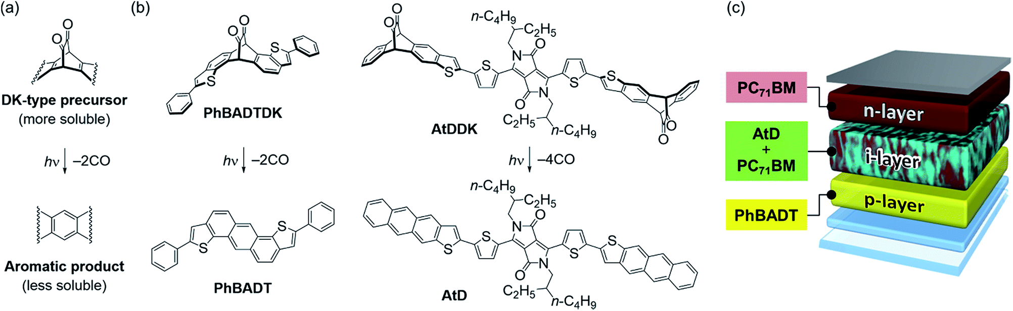 | ||
| Fig. 1 (a) General scheme of the photo-induced decarbonylative aromatization employed in the photoprecursor approach; (b) chemical structures of the newly synthesized DK-type photoprecursors PhBADTDK and AtDDK, and their photoreaction products PhBADT and AtD; (c) schematic illustration of the p–i–n-type OPV evaluated in this work. | ||
Importantly, when solubility of the resulting acene compound is sufficiently low, another material can be deposited on top of it as a solution. Our proof-of-concept study demonstrated that the photoprecursor approach could be applied to the preparation of p–i–n-type photovoltaic active layers where a p:n blend (intermixed layer or i-layer) was sandwiched between neat p- and n-type materials (p- and n-layers).13 This triple-layer structure was predicted to afford higher photovoltaic efficiency as compared to the p:n-blend monolayer system (i.e., standard bulk-heterojunction (BHJ) system) owing to the combination of efficient charge-carrier generation in the i-layer and swift charge-carrier extraction through the p- and n-layers. Indeed, the p–i–n devices prepared via the photoprecursor approach afforded up to more than three times higher power-conversion efficiencies (PCEs) as compared to the corresponding BHJ devices. This significant improvement manifests the importance of controlling the vertical composition profile in the active layer, which is often hard to achieve with conventional solution processes.
Multilayer structures such as p–i–n are also attractive in other aspects. For instance, different layers can be independently optimized depending on their required functions; specifically, swift and selective transport of photogenerated charge carriers for the p- and n-layers, or efficient photoabsorption and charge-carrier generation for the i-layer.2 Organic semiconductors can take full advantage of this benefit because of their highly diverse and tunable nature. Another advantage is the high freedom in optimizing thin-film optics. As the thickness of each sublayer can be altered on demand, the active-layer structure may be tuned such that photons are selectively and effectively absorbed at the right position in order to make maximum use of incident sunlight.17
By taking into account these benefits, as well as the compatibility with wet processing and the mildness of the post-deposition photoreaction, we expect that the photoprecursor approach may serve as an effective means for preparing efficient, large-area and flexible OPVs. Towards this goal, the present work significantly extends the scope of the photoprecursor approach from the previous proof-of-concept report.13 The following describes synthesis and photoreactivity of two new DK-type derivatives of small-molecule organic semiconductors PhBADT and AtD, which are specifically chosen/designed for the p- and i-layers in p–i–n-type OPVs, respectively (Fig. 1b and c). We also compared different types of active layers in order to confirm the previously suggested advantages accompanying the control over the vertical composition profile in the active layer.13,17–21 Overall, this contribution illustrates the effectiveness of the photoprecursor approach toward achieving well-performing OPVs having the right material in the right place.
Results and discussion
Molecular design and synthesis
The p-layer in p–i–n-type OPVs should have high transparency and hole-transport capability. Herein, PhBADT is the material of choice for the p-layer, because it is transparent in a wide range of the visible region.22 PhBADT is also known to form three dimensionally extended π–π contacts in the solid state, which is favourable in achieving effective hole-transport paths.23 Furthermore, PhBADT is scarcely soluble, while the corresponding DK-type photoprecursor PhBADTDK is well soluble. This is highly important in the context of constructing multilayer structures via the photoprecursor approach. PhBADTDK is accessible in three steps from PhBADT as shown in Scheme 1a. The conversion of PhBADTDK to PhBADT has been spectroscopically confirmed both in solution and in the thin-film state (Fig. S1, ESI†).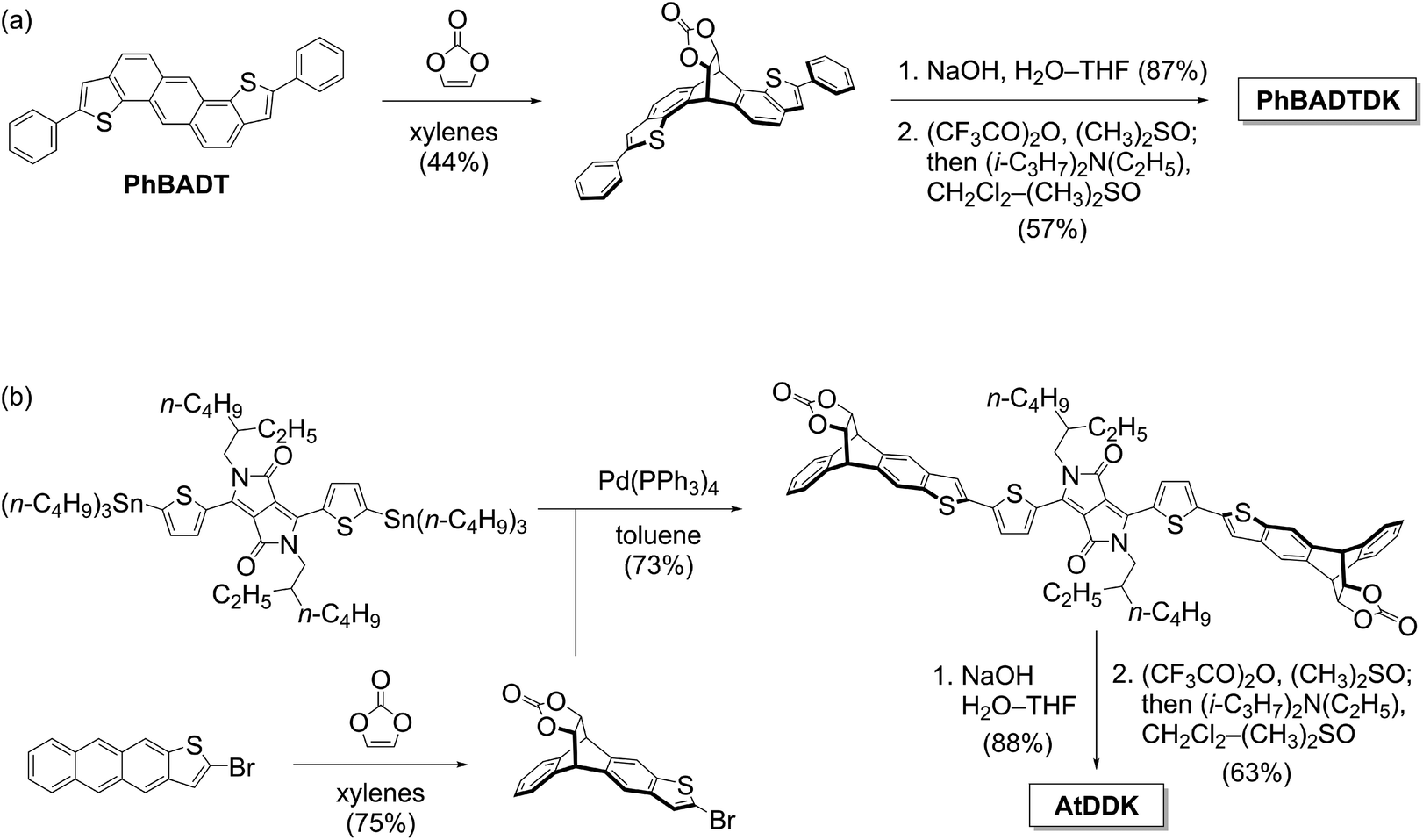 | ||
| Scheme 1 Synthesis of the photoprecursors. (a) PhBADTDK; (b) AtDDK. | ||
On the other hand, the i-layer should efficiently absorb the sunlight and generate charge carriers. AtD, a conjugate of anthrathiophene (At) and dithienyldiketopyrrolopyrrole (DTDPP), is newly designed to fit the needs for the photovoltaic process and the wet processing via the photoprecursor approach. DFT calculations have shown that the DTDPP unit is the main contributor to both the highest occupied molecular orbital (HOMO) and the lowest unoccupied molecular orbital (LUMO) of AtD (see the next section and Fig. S3†). Therefore, the configuration of AtD does not follow the commonly employed “weak donor/strong acceptor” design in which the donor unit is a main contributor to the HOMO, while the acceptor unit (DTDPP is among the common examples) to the LUMO.24 Rather, the central DTDPP group in AtD serves as a primary dye unit ensuring high light absorptivity, while the two At units serve as a modulator of the frontier-orbital energy levels through π-extension. The At units are also the points of introducing the photo-reactive DK group. Having two DK units assures high contrast in solubility between the photoprecursor (AtDDK, well soluble) and the photoreaction product (AtD, scarcely soluble). The synthesis of AtDDK can be achieved via the Stille coupling between the corresponding derivatives of DTDPP and At units, followed by hydrolysis and Swern oxidation to generate the DK units (Scheme 1b). The conversion of AtDDK to AtD has been confirmed similarly to the case of PhBADTDK (Fig. S2†).
Electronic structures
The calculated frontier-orbital coefficient distributions of PhBADT and AtD are shown in Fig. 2a and b. In PhBADT, both the HOMO and LUMO delocalize over the whole π-framework, even though the phenyl groups are not coplanar against the central anthradithiophene core (the dihedral angle is 27°, Fig. S4a†). On the other hand, the frontier orbitals of AtD relatively localize at the DTDPP unit as mentioned in the previous section, although its π-framework is optimized to be fully coplanar (Fig. S4b†). Nonetheless, the HOMO of AtD managed to extend to the end of At units, suggesting that it would be still possible to form effective intermolecular HOMO–HOMO contacts and thus hole-transport paths in the solid state.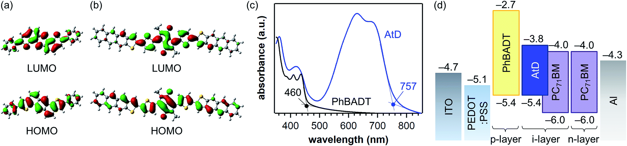 | ||
| Fig. 2 (a and b) Frontier-orbital coefficient distribution in PhBADT and AtD calculated at the B3LYP/6-31G(d) level of theory. Note that the ethylhexyl groups of AtD are simplified to methyl for saving the calculation time. (c) Photoabsorption spectra of thin films of PhBADT and AtD prepared by the photoprecursor approach. (d) Energy-level diagram of PhBADT and AtD along with PC71BM and electrode materials. The values are adopted from the literature26 except those for PhBADT and AtD. The HOMO levels of PhBADT and AtD were determined by photoelectron yield spectroscopy in air and the LUMO levels were calculated to be “HOMO + absorption onset energy”. See the ESI† for experimental details. | ||
Shown in Fig. 2c and d are the UV-Vis absorption spectra and experimentally determined frontier-orbital energies of PhBADT and AtD in the thin-film state. The absorption onset of PhBADT is located at 460 nm, while AtD has a strong absorption at 600–700 nm with an onset around 760 nm. Note that AtD has, despite its simple structure, a similar photoabsorption range to those of high-performance photoabsorbers such as PTB7-Th.25 In addition, AtD is rather transparent around 470–500 nm at which the absorption of the photo-reactive DK unit is located. This is beneficial for minimizing the interruption of the intended photo-induced decarbonylation by the masking effect of the photoreaction product. With regard to the frontier-orbital energy levels, there is no offset between the HOMOs of PhBADT and AtD, and thus barrier-free extraction of holes from the i-layer to the p-layer is expected. On the other hand, the LUMO–LUMO offset between AtD and PC71BM has been estimated to be 0.2 eV (−3.8 eV for AtD and −4.0 eV for PC71BM26), which is around the smallest possible for ensuring efficient electron transfer from the p-type material to the n-type material. Thus, AtD is tuned to have ideal frontier-orbital energies as a partner of PC71BM.24 Overall, these computational and experimental results suggest that PhBADT, AtD, and PC71BM constitute an optimal ternary system in terms of the molecular electronic structure for constructing a p–i–n photovoltaic layer.
Photovoltaic performance
The p–i–n OPVs comprising PhBADT, AtD, and PC71BM were fabricated via the photoprecursor approach as schematically illustrated in Fig. 3. The p-layer was deposited by spin-coating of PhBADTDK in chloroform followed by irradiation with a blue LED (470 nm) to form PhBADT. The i-layer was deposited in a similar manner with chloroform as the cast solvent, but from a blend solution of AtDDK and PC71BM instead of PhBADTDK. The ratio between AtDDK and PC71BM in the cast solution was optimized to be 1![[thin space (1/6-em)]](https://www.rsc.org/images/entities/char_2009.gif) :1 by weight (Table S1†) and kept the same throughout this study. Lastly, PC71BM was spin-coated as a chloroform solution to complete the p–i–n structure.
:1 by weight (Table S1†) and kept the same throughout this study. Lastly, PC71BM was spin-coated as a chloroform solution to complete the p–i–n structure.
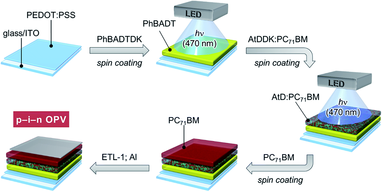 | ||
| Fig. 3 Schematic description of the procedure for fabricating p–i–n-type OPVs through the photoprecursor approach. ETL-1 is a fullerene-based solution-processable cathode buffer reported by Li et al.27 | ||
The thickness of each sublayer was controlled by changing the concentration of cast solution, and the best photovoltaic performance was obtained when p, i and n-layers were deposited by using solutions of 1, 9 and 7 mg mL−1, respectively. The ratio of the three components in the resulting thin film was roughly estimated to be about 1:3:10 through fitting analysis of absorption spectra (Fig. S6†). Note here that the exact thickness of each sublayer is hard to define in the present case because dissolution and mixing cannot be fully avoided. Nonetheless, the advantage of sequential deposition of different materials over the one-time deposition of a mixture is obvious as described below. We expect that higher control over the sublayer thickness would be achieved by employing an n-type material that can be completely “insolubilized” via the precursor approach. Work along this line is underway in our group,10 and the result will be reported elsewhere in due course.
The maximum power conversion efficiency (PCE) achieved in thus-prepared p–i–n-type active layer was 4.7% associated with a short-circuit current density (JSC) of 10.6 mA cm−1, an open-circuit voltage (VOC) of 0.89 V, and a fill factor (FF) of 49.8% (Table 1, Entry 1). As compared to the previously reported proof-of-concept system (PCE = 2.9%, JSC = 5.8 mA cm−1, VOC = 0.91 V, FF = 55%),13 the increase in JSC is significant. This can be attributed mainly to the improved photoabsorption capability of AtD in comparison with 2,6-bis[5′-(2-ethylhexyl)-(2,2′-bithiophen)-5-yl]anthracene (EH-DBTA, see Fig. S5† for the chemical structure). Indeed, the photovoltaic response in the present device covers the whole range of visible light (350–750 nm) as a result of complementary photoabsorption of AtD and PC71BM (Fig. 4b). In addition, the employment of PhBADT, instead of the prototype p-layer material 2,6-di(2-thienyl)anthracene (DTA, see Fig. S5† for the chemical structure) has enhanced JSC and FF (Table S2†). Thus, the layer-by-layer solution process via the photoprecursor approach is successfully advanced from a proof-of-concept demonstration to the stage of material optimization for achieving efficient OPVs.
| Entry | Active layer structurec | J SC (mA cm−2) | V OC (V) | FFd (%) | PCEd (%) | PCEavee (%) | R S (Ω cm2) | R P (Ω cm2) |
|---|---|---|---|---|---|---|---|---|
|
a Measured under simulated AM1.5G illumination at 100 mW cm−2.
b General device structure: [ITO/PEDOT:PSS (30 nm)/active layer/ETL-1/Al (80 nm)].
c Concentrations of cast solutions: PhBADTDK for p-layer, 1 mg mL−1; AtDDK:PC71BM (1:1) for i-layer, 9 mg mL−1; PC71BM for n-layer, 7 mg mL−1. All these solutions are in chloroform.
d Parameters of the best-performing cells.
e Averages and standard deviations calculated from at least four devices.
f
R
S, series resistance; RP, parallel resistance.
g Annealed with THF vapor for 120 s.
|
||||||||
| 1 | p–i–n | 10.6 | 0.89 | 49.8 | 4.7 | 4.3 ± 0.3 | 16 | 424 |
| 2 | BHJ | 1.6 | 0.83 | 23.5 | 0.30 | 0.29 ± 0.02 | 433 | 465 |
| 3 | p–i | 2.8 | 0.92 | 24.6 | 0.63 | 0.58 ± 0.09 | 213 | 307 |
| 4 | i–n | 9.7 | 0.89 | 48.1 | 4.1 | 3.9 ± 0.4 | 21 | 423 |
| 5 | p–i–n (with SVA)g | 12.7 | 0.88 | 52.6 | 5.9 | 5.5 ± 0.3 | 11 | 411 |
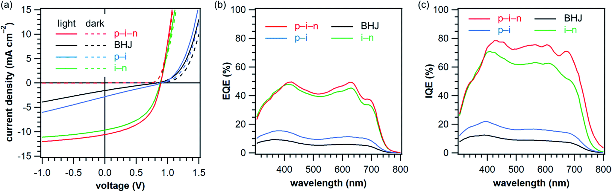 | ||
| Fig. 4 Photovoltaic response of the OPVs prepared without annealing treatment (Entries 1–4 in Table 1). (a) J–V curves; (b) EQE spectra; (c) IQE spectra. Data are of the best-performing cell in each active-layer structure and obtained under simulated AM1.5G illumination at 100 mW cm−2. EQE: external quantum efficiency, IQE: internal quantum efficiency. | ||
We have then examined the effectiveness of the p–i–n structure by comparing it with the corresponding BHJ monolayer device. In addition, partial structures of the p–i–n active layer, namely p–i and i–n bilayers, were also evaluated.
The results are summarized in Table 1 and Fig. 4. Note that the concentrations of cast solutions were kept the same as those for the p–i–n device to allow direct comparison, but optimized for each active-layer structures except the case of p–i–n.
The BHJ system showed a considerably lower PCE of 0.30% (JSC = 1.6 mA cm−2, VOC = 0.83 V, and FF = 23.5%) than the p–i–n device (Table 1, Entry 2). A high series resistance (RS) is apparent in this case, indicating the lack of effective charge-carrier paths in the active layer. This is also reflected to the significantly deteriorated JSC and FF. In turn, the low PCE of the BHJ device clearly demonstrates the advantage of employing the p–i–n structure when the morphology of the BHJ layer is far from ideal.
In the p–i device, photovoltaic efficiency was improved by approximately twice (PCE = 0.63%) as compared to the BHJ device. This improvement can be attributed mainly to the increase in JSC from 1.6 to 2.8 mA cm−2 (Table 1, Entry 3). The external and internal quantum efficiencies (EQE and IQE) were uniformly enhanced over the whole range of active wavelengths (Fig. 4b and c), and thus the photons absorbed by AtD and PC71BM should have equally contributed to the higher JSC. Here, the IQE values were estimated using the method employed by Yu et al.28 Although this method does not account for parasitic absorption and thus can underestimate the “true” quantum efficiency,29 the estimated IQEs would still provide useful information on systematic comparison between devices.
On the other hand, the photoabsorption by p-layer should not significantly affect the EQE because of its short absorption onset wavelength and thinness (<10 nm). A possible explanation for the enhancement in JSC would be that the charge recombination was reduced by the selective extraction of holes into the p-layer. Another likely cause is the blocking effect of the wide-band-gap p-layer which keeps excitons from being quenched in the PEDOT:PSS buffer.30 At the same time, however, such positive effects should be limited to an adjacent segment around the p–i interface, and the overall photovoltaic process is still low because of the unfavourable morphology in the i-layer as evidenced by the low FF and high RS.
The i–n system afforded a much higher PCE of 4.1% than the BHJ system (Table 1, Entry 4). As the JSC and FF were both largely increased (from 1.6 to 9.7 mA cm−2 and from 23.5 to 48.1%, respectively), improvement in charge-extraction efficiency should be a main reason for the significantly higher PCE. In this case, a drastic change of the vertical composition profile in the i-layer can be expected, because the insoluble p-type material (AtD) settling on the soluble n-type material (PC71BM) should be washed away at least partially during the deposition of the n-layer from a chloroform solution. Note here that PC71BM is newly supplied from the cast solution, and thus the BHJ-type structure in the i-layer should be mostly maintained, as indicated by the similarity in the EQE profile between i–n and p–i–n devices. This would lead to the formation of an active layer in which the concentration of the n-type material increases from the bottom (anode side) to the top (cathode side). Such a vertical phase separation has been suggested as being favourable for the charge-carrier collection process.31–33 It should also be noted here that the sequential solution deposition enables preparing this type of material distribution by design, rather than extensive screening of deposition conditions for each different combination of materials. Another factor potentially influencing is the annealing effect by the cast solvent (chloroform) which improves the phase purity and thus charge-carrier transport efficiency in the i-layer. This latter aspect is examined in more detail in the next section. The photoabsorption by the n-layer, on the other hand, would not be a main factor in the improvement of photocurrent, because the EQE has increased throughout the whole of active wavelengths rather than only those corresponding to the PC71BM absorption.
Annealing of BHJ layers prepared by the photoprecursor approach
The effect of solvent vapor annealing (SVA) on the AtD:PC71BM BHJ system was screened using several different solvents (Table S3†). This preliminary examination showed that SVA with chloroform, as mentioned above, considerably improved PCE (Table S3, Entry S7†). An even better result was obtained with tetrahydrofuran (THF), affording a five times higher PCE as compared to the non-annealed device prepared in the same batch (Table S3, Entry S9†). The SVA treatment in this screening was performed after the photoreaction of AtDDK to AtD. Thus, these results demonstrate that hardly soluble molecules equipped with minimal flexible substituents can still rearrange to a considerable degree in the solid state by merely exposing to solvent vapor for a relatively short period (60 s). At the same time, preliminary experiments also showed that other common morphology-control techniques such as thermal annealing and the use of a high-boiling-point additive were not effective in the present system (Tables S4 and S5†).Analysis of the surface morphology by atomic force microscopy (AFM) showed that SVA with THF increased the grain size and surface roughness (Fig. 5a and b). Namely, grains of tens of nanometers in diameter became apparent after the SVA treatment, while the pre-annealing film showed a much finer texture. In addition, the root-mean-square (RMS) roughness increased from 0.32 to 0.48 nm. Such a morphological change has been often related to the increase in phase purity and thus charge-carrier transport efficiency,7 which seems also the case for the present AtD:PC71BM system wherein JSC and FF have been largely enhanced upon SVA.
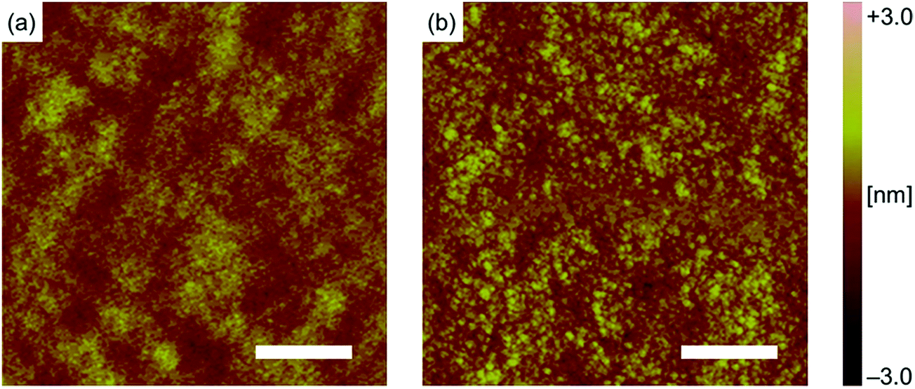 | ||
| Fig. 5 Tapping-mode AFM images of AtD:PC71BM (1:1) blend films before (a) and after (b) SVA with THF. The scale bars correspond to 0.5 μm. The RMS values of surface roughness are 0.32 and 0.48 nm for (a) and (b), respectively. | ||
The SVA with THF was then applied to the p–i–n system. This treatment was found best to apply after deposition of the i-layer, while it was not as effective after deposition of the n-layer (Table S6†). The duration of SVA was optimized at 120 s, although the process window was rather wide, with the PCE changing little within the range of 60–180 s (Table S7†). The annealing significantly improved the photovoltaic efficiency of the p–i–n device to afford the maximum PCE of 5.9% (Entry 5 in Table 1, and Fig. 6a). The improvement can be ascribed mainly to the enhanced JSC (10.6 → 12.7 mA cm−2) and FF (49.8 → 52.6%). Fig. 6b shows the photoabsorption, EQE, and IQE spectra of the best-performing p–i–n cell prepared with THF SVA. The EQE was enhanced at all the active wavelengths and the maximum EQE reached 60%, while it was around 50% without SVA (Fig. 4b), indicating a considerable improvement in charge-carrier collection efficiency. This is well reflected in the high IQE, the maximum of which reaches almost 100%.
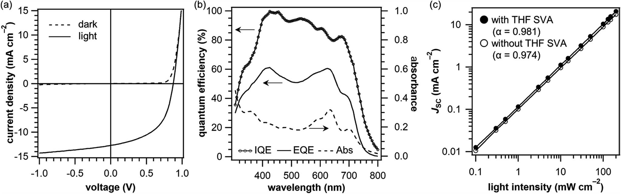 | ||
| Fig. 6 Photovoltaic characteristics of p–i–n OPVs. (a) J–V curves and (b) photoabsorption, EQE and IQE spectra of the best-performing p–i–n OPV prepared with THF SVA; (c) light-intensity dependence of JSC of the best-performing p–i–n devices prepared with THF SVA; (c) light-intensity dependence of JSC of the best-performing p–i–n devices prepared with and without THF SVA. The α values are 0.981 for the device with SVA and 0.974 without SVA. | ||
The variation in JSC as a function of illumination intensity was also measured for the p–i–n devices with and without THF SVA (Fig. 6c). In general, the power-law dependence of JSC upon light intensity (JSC ∝ Iα where α is an exponential factor) is observed for OPVs, and α = 1 indicates an efficient sweep-out of charge carriers prior to recombination. The α values are as high as 0.981 and 0.974 for the devices with and without THF SVA, respectively. Thus, the p–i–n device without SVA already had a relatively high efficiency of charge-carrier collection, and the efficiency was further enhanced upon THF SVA.
Conclusions
In summary, this contribution has clearly demonstrated that the photoprecursor approach is applicable to a wide variety of organic semiconductors from simple wide-band-gap compounds as PhBADT to π-extended narrow-band-gap compounds as AtD. This versatility enabled the controlled deposition of ternary photovoltaic layers containing independently optimized two different p-type materials. The advantage of the thus-obtained p–i–n-type OPV was confirmed through the systematic comparison of different active-layer structures, wherein the p–i–n device afforded a one-order higher efficiency than the corresponding BHJ device (4.7% vs. 0.3%). This increase in PCE can be ascribed to the improved vertical composition profile, which enables more efficient charge-carrier collection, as manifested by the higher JSC and FF.31–33 It has also been shown that the solid-state molecular arrangement in BHJ layers can be significantly modified without heating, even when molecules are equipped with only minimal flexible substituents so that they are insoluble. Accordingly, SVA of the AtD:PC71BM layer considerably improved the PCE of the p–i–n OPV (4.7 → 5.9%). The 5.9% PCE is indeed the highest reported for p–i–n-type OPVs prepared by solution process,18,19 and importantly even higher PCEs can be expected upon further optimization of the active-layer structure as indicated by the increasing photocurrent at negative bias voltages (Fig. 6a).It would be worth emphasizing that the present photoprecursor approach is characterized by the mildness of the post-deposition reaction in which only visible-light irradiation is required. In relation to this aspect, it is known that fullerenes and their derivatives undergo photo-induced [2 + 2] addition in the solid state. Indeed, the photoreactivity of fullerenes has been a subject of several studies concerning the stability of BHJ OPVs containing PC61BM.34–40 By contrast, PC71BM is reported to be much less susceptive to the [2 + 2] reaction owing to the lower number of reactive double bonds.41,42 In the present case of photoprecursor approach, any sign of the [2 + 2] dimerization or oligomerization has not been detected in terms of the change in photoabsorption34 and solubility43,44 during the in situ photoreaction (Fig. S7†). It is therefore assumed that the effect of the [2 + 2] addition would not be significant, if any, to the performance of the OPVs prepared in this work.
Another advantage of the photoprecursor approach is that it allows molecules to be free from extensive decollation with flexible and insulating substituents, enabling efficient intermolecular π–π contact in the solid state. This will be highly beneficial in enhancing electronic performance and morphological stability of organic semiconducting thin films. Now that its material scope is largely extended, we postulate that the photoprecursor approach can serve as an effective means for the controlled preparation of high-performance photovoltaic layers and other multicomponent organic semiconductors having “the right material in the right place”.
Conflicts of interest
The authors declare no competing financial interest.Acknowledgements
This research was supported by the CREST program of the Japan Science and Technology Agency (JST), Grants-in-Aid for Scientific Research (KAKENHI) (No. JP26105004, JP16H02286, JP16K17949 and JP17H03134) from the Japan Society for the Promotion of Science (JSPS), Japan Regional Innovation Strategy Program by the Excellence (J-RISE) sponsored by JST, NAIST foundation, Izumi science and technology foundation, and the program for promoting the enhancement of research universities in NAIST supported by MEXT. We thank Ms Yoshiko Nishikawa at NAIST for assistance in mass spectroscopic measurements.Notes and references
- K. Leo, Elementary Processes in Organic Photovoltaics, Springer International Publishing, 2016 Search PubMed.
- Y. Wang and X. Zhan, Adv. Energy Mater., 2016, 6, 1600414 CrossRef.
- Q. Wan, X. Guo, Z. Wang, W. Li, B. Guo, W. Ma, M. Zhang and Y. Li, Adv. Funct. Mater., 2016, 26, 6635–6640 CrossRef.
- G. Ren, E. Ahmed and S. A. Jenekhe, Adv. Energy Mater., 2011, 1, 946–953 CrossRef.
- J. S. Moon, C. J. Takacs, S. Cho, R. C. Coffin, H. Kim, G. C. Bazan and A. J. Heeger, Nano Lett., 2010, 10, 4005–4008 CrossRef PubMed.
- L. A. Perez, J. T. Rogers, M. A. Brady, Y. Sun, G. C. Welch, K. Schmidt, M. F. Toney, H. Jinnai, A. J. Heeger, M. L. Chabinyc, G. C. Bazan and E. J. Kramer, Chem. Mater., 2014, 26, 6531–6541 CrossRef.
- K. A. O'Hara, D. P. Ostrowski, U. Koldemir, C. J. Takacs, S. E. Shaheen, A. Sellinger and M. L. Chabinyc, ACS Appl. Mater. Interfaces, 2017, 9, 19021–19029 CrossRef PubMed.
- Y. Zhao, Z. Xie, Y. Qu, Y. Geng and L. Wang, Appl. Phys. Lett., 2007, 90, 043504 CrossRef.
- A. Sharenko, M. Kuik, M. F. Toney and T.-Q. Nguyen, Adv. Funct. Mater., 2014, 24, 3543–3550 CrossRef.
- K. Kawajiri, T. Kawanoue, M. Yamato, K. Terai, M. Yamashita, M. Furukawa, N. Aratani, M. Suzuki, K. Nakayama and H. Yamada, ECS J. Solid State Sci. Technol., 2017, 6, M3068–M3074 CrossRef.
- C. Quinton, M. Suzuki, Y. Kaneshige, Y. Tatenaka, C. Katagiri, Y. Yamaguchi, D. Kuzuhara, N. Aratani, K. Nakayama and H. Yamada, J. Mater. Chem. C, 2015, 3, 5995–6005 RSC.
- S. Masuo, W. Sato, Y. Yamaguchi, M. Suzuki, K. Nakayama and H. Yamada, Photochem. Photobiol. Sci., 2015, 14, 883–890 RSC.
- Y. Yamaguchi, M. Suzuki, T. Motoyama, S. Sugii, C. Katagiri, K. Takahira, S. Ikeda, H. Yamada and K. Nakayama, Sci. Rep., 2014, 4, 7151 CrossRef PubMed.
- M. Suzuki, T. Aotake, Y. Yamaguchi, N. Noguchi, H. Nakano, K. Nakayama and H. Yamada, J. Photochem. Photobiol., C, 2014, 18, 50–70 CrossRef.
- H. Yamada, Y. Yamaguchi, R. Katoh, T. Motoyama, T. Aotake, D. Kuzuhara, M. Suzuki, T. Okujima, H. Uno, N. Aratani and K. Nakayama, Chem. Commun., 2013, 49, 11638–11640 RSC.
- M. Suzuki, Y. Yamaguchi, K. Takahashi, K. Takahira, T. Koganezawa, S. Masuo, K. Nakayama and H. Yamada, ACS Appl. Mater. Interfaces, 2016, 8, 8644–8651 CrossRef PubMed.
- B. Maennig, J. Drechsel, D. Gebeyehu, P. Simon, F. Kozlowski, A. Werner, F. Li, S. Grundmann, S. Sonntag, M. Koch, K. Leo, M. Pfeiffer, H. Hoppe, D. Meissner, N. S. Sariciftci, I. Riedel, V. Dyakonov and J. Parisi, Appl. Phys. A: Mater. Sci. Process., 2004, 79, 1–14 CrossRef.
- Y. Matsuo, Y. Sato, T. Niinomi, I. Soga, H. Tanaka and E. Nakamura, J. Am. Chem. Soc., 2009, 131, 16048–16050 CrossRef PubMed.
- T. L. Chen, J. J.-A. Chen, L. Catane and B. Ma, Org. Electron., 2011, 12, 1126–1131 CrossRef.
- M. Hiramoto, H. Fujiwara and M. Yokoyama, Appl. Phys. Lett., 1991, 58, 1062–1064 CrossRef.
- B. Ray and M. A. Alam, Sol. Energy Mater. Sol. Cells, 2012, 99, 204–212 CrossRef.
- A. Pietrangelo, B. O. Patrick, M. J. MacLachlan and M. O. Wolf, J. Org. Chem., 2009, 74, 4918–4926 CrossRef PubMed.
- Y. Yi, L. Zhu and J.-L. Brédas, J. Phys. Chem. C, 2012, 116, 5215–5224 CrossRef.
- H. Zhou, L. Yang, S. Stoneking and W. You, ACS Appl. Mater. Interfaces, 2010, 2, 1377–1383 CrossRef PubMed.
- S. Zhang, L. Ye, W. Zhao, D. Liu, H. Yao and J. Hou, Macromolecules, 2014, 47, 4653–4659 CrossRef.
- Y. Liu, C.-C. Chen, Z. Hong, J. Gao, Y. (Michael) Yang, H. Zhou, L. Dou, G. Li and Y. Yang, Sci. Rep., 2013, 3, 3356 CrossRef PubMed.
- C.-Z. Li, C.-C. Chueh, H.-L. Yip, K. M. O'Malley, W.-C. Chen and A. K.-Y. Jen, J. Mater. Chem., 2012, 22, 8574–8578 RSC.
- Y. Liang, Z. Xu, J. Xia, S.-T. Tsai, Y. Wu, G. Li, C. Ray and L. Yu, Adv. Mater., 2010, 22, E135–E138 CrossRef PubMed.
- A. Armin, M. Velusamy, P. Wolfer, Y. Zhang, P. L. Burn, P. Meredith and A. Pivrikas, ACS Photonics, 2014, 1, 173–181 CrossRef.
- M. Hirade and C. Adachi, Appl. Phys. Lett., 2011, 99, 153302 CrossRef.
- Z. Xiao, Y. Yuan, B. Yang, J. VanDerslice, J. Chen, O. Dyck, G. Duscher and J. Huang, Adv. Mater., 2014, 26, 3068–3075 CrossRef PubMed.
- X. Guo, N. Zhou, S. J. Lou, J. Smith, D. B. Tice, J. W. Hennek, R. P. Ortiz, J. T. L. Navarrete, S. Li, J. Strzalka, L. X. Chen, R. P. H. Chang, A. Facchetti and T. J. Marks, Nat. Photonics, 2013, 7, 825–833 CrossRef.
- L.-M. Chen, Z. Xu, Z. Hong and Y. Yang, J. Mater. Chem., 2010, 20, 2575–2598 RSC.
- L. N. Inasaridze, A. I. Shames, I. V. Martynov, B. Li, A. V. Mumyatov, D. K. Susarova, E. A. Katz and P. A. Troshin, J. Mater. Chem. A, 2017, 5, 8044–8050 RSC.
- I. F. Domínguez, A. Distler and L. Lüer, Adv. Energy Mater., 2017, 7, 1601320 CrossRef.
- T. Heumueller, W. R. Mateker, A. Distler, U. F. Fritze, R. Cheacharoen, W. H. Nguyen, M. Biele, M. Salvador, M. von Delius, H.-J. Egelhaaf, M. D. McGehee and C. J. Brabec, Energy Environ. Sci., 2016, 9, 247–256 RSC.
- G. E. Morse, A. Tournebize, A. Rivaton, T. Chassé, C. Taviot-Gueho, N. Blouin, O. R. Lozman and S. Tierney, Phys. Chem. Chem. Phys., 2015, 17, 11884–11897 RSC.
- H. C. Wong, Z. Li, C. H. Tan, H. Zhong, Z. Huang, H. Bronstein, I. McCulloch, J. T. Cabral and J. R. Durrant, ACS Nano, 2014, 8, 1297–1308 CrossRef PubMed.
- A. Distler, T. Sauermann, H.-J. Egelhaaf, S. Rodman, D. Waller, K.-S. Cheon, M. Lee and D. M. Guldi, Adv. Energy Mater., 2014, 4, 1300693 CrossRef.
- F. Piersimoni, G. Degutis, S. Bertho, K. Vandewal, D. Spoltore, T. Vangerven, J. Drijkoningen, M. K. V. Bael, A. Hardy, J. D'Haen, W. Maes, D. Vanderzande, M. Nesladek and J. Manca, J. Polym. Sci., Part B: Polym. Phys., 2013, 51, 1209–1214 CrossRef.
- P. C. Eklund, A. M. Rao, P. Zhou, Y. Wang and J. M. Holden, Thin Solid Films, 1995, 257, 185–203 CrossRef.
- A. M. Rao, M. Menon, K.-A. Wang, P. C. Eklund, K. R. Subbaswamy, D. S. Cornett, M. A. Duncan and I. J. Amster, Chem. Phys. Lett., 1994, 224, 106–112 CrossRef.
- A. Dzwilewski, T. Wågberg and L. Edman, J. Am. Chem. Soc., 2009, 131, 4006–4011 CrossRef PubMed.
- J. Wang, C. Larsen, T. Wågberg and L. Edman, Adv. Funct. Mater., 2011, 21, 3723–3728 CrossRef.
Footnote |
| † Electronic supplementary information (ESI) available. See DOI: 10.1039/c8sc01799a |
| This journal is © The Royal Society of Chemistry 2018 |