
 Open Access Article
 This Open Access Article is licensed under a Creative Commons Attribution-Non Commercial 3.0 Unported Licence
Chemical transformations at the nanoscale: nanocrystal-seeded synthesis of β-Cu2V2O7 with enhanced photoconversion efficiencies†
Chethana
Gadiyar
a,
Michal
Strach
a,
Pascal
Schouwink
b,
Anna
Loiudice
a and
Raffaella
Buonsanti
 *a
*a
aLaboratory of Nanochemistry for Energy (LNCE), Department of Chemical Sciences and Engineering, École Polytechnique Fédérale de Lausanne, CH-1950 Sion, Switzerland. E-mail: raffaella.buonsanti@epfl.ch
bDepartment of Chemical Sciences and Engineering, École Polytechnique Fédérale de Lausanne, CH-1950 Sion, Switzerland
First published on 29th May 2018
Abstract
Nanocrystal-seeded synthesis relies on the reaction of nanocrystal seeds with a molecular precursor and it can be regarded as the link between sol–gel and solid-state chemistries. This synthesis approach aims at accessing compositionally complex materials, yet to date its full potential remains unexploited. Herein, surface oxidized Cu nanocrystal seeds with diameters from 6 nm to 70 nm are reacted with vanadium acetylacetonate to form β-Cu2V2O7 with a tunable grain size ranging from 29 nm to 63 nm. In situ X-ray diffraction measurements evidence the occurrence of a solid-state reaction between the NC seeds and the vanadium oxide formed during the annealing. The variation of the ion diffusion lengths, the homogeneity of the precursor solution and the number of nucleation sites with the NC seed size explains the lower formation temperature, the smaller grain size and the higher grain size monodispersity of β-Cu2V2O7 as the seed size decreases. Finally, the tunability afforded by the nanocrystal-seeded synthesis provides a unique opportunity to correlate the photoelectrochemical performance with the grain size in a size regime close to the charge carrier diffusion length of β-Cu2V2O7 (20–40 nm). The net photocurrent density peaks when the grain size is 39 nm by reaching 0.23 mA cm−2 at 1.23 V vs. RHE in the presence of a hole scavenger. While still far from the theoretical limit, this result overcomes the current state-of-the-art for β-Cu2V2O7. An interesting double fold increase in the photocurrent is found in mixed phase β-Cu2V2O7/CuV2O6 samples, suggesting that nanostructuring and heterostructuring are beneficial to the performance.
Introduction
Multinary metal oxides are emerging as key materials to advance diverse applications ranging from batteries to flexible electronics, catalysis and plasmonics.1–12 Achieving control over crystalline phases, stoichiometry, grain size and morphology is of the uttermost importance considering the correlation of these structural features with the physical–chemical properties and with the device performance. This urgent need requires novel synthetic approaches, which include various seeding strategies, photochemical synthesis and nanoscale solid-state reactions.1–13 To cite one example, Bretos et al. introduced crystalline PbTiO3 nanoseeds in a sol–gel mixture of molecular precursors to successfully reduce the crystallization temperature of Pb(Zr0.52Ti0.48)O3, thus enabling its integration on flexible substrates.5 As a second example, the development of a photochemical metal–organic deposition has given access to an amorphous mixed metal oxide with excellent catalytic properties for oxygen evolution.3 Another example comes from Chuang et al. who have exploited the nanoscale solid state reaction between ZnO and GaN nanocrystals to tune the composition and the band gap of (Ga1−xZnx)(N1−xOx), a material with intriguing optical properties relevant for solar fuel generation.9–12 Finally, our group has recently developed a nanocrystal-seeded growth approach wherein BixSb1−x nanocrystalline thin films react with vanadium precursor to afford a new photoanode material, BiV1−xSbxO4.13 This compound had been predicted by theoretical calculations but attempts to synthesize it by more conventional approaches, such as sol–gel, solid-state synthesis and spray pyrolysis, had been unsuccessful.Copper vanadates have been recently highlighted as promising photoanode materials for tandem photoelectrochemical devices.14 There are 26 phases of copper vanadate listed in the Inorganic Crystal Structure database with different structural and opto-electronic properties. Various techniques like solid state synthesis,15,16 solution approaches,17–20 physical vapor deposition,21–23 electrospraying,24 sol–gel methods25 have been applied to access different crystalline phases within this family of compounds.
Several stoichiometries of copper vanadates have been obtained by varying the synthesis parameters such as the precursor ratio and the annealing temperature. The reported band gaps are in the range 1.8–2.1 eV, suggesting the possibility to reach maximum photocurrent densities up to 13 mA cm−2. Nevertheless, the values reported so far for different copper vanadates in the presence of a hole scavenger are usually below 0.1 mA cm−2, thus much lower than this theoretical limit.17–23 In previous studies, the high annealing temperatures above 450 °C have resulted in grain sizes varying from 200 nm to 1 μm.17–25 These grain sizes are much larger than the charge carrier diffusion length (20–40 nm), which may be among the causes for the low photocurrent density in these studies.22 Thus, synthesizing copper vanadates with monodisperse grain sizes ≤40 nm is expected to improve the photoconversion efficiency of this promising material. More importantly, tuning the grain size in this range will lead towards a more fundamental understanding of the intimate relationship between grain size and performance. Electrodeposition has been demonstrated to be a very powerful technique to access nanoporous ternary metal oxide photoelectrodes, yet the grain size monodispersity and tunability are still limited.20,26,27 Therefore, expanding the available methods to synthesize multication oxides is highly desirable if one aims at correlating morphological parameters with performance metrics.
Experimental
Materials
Copper(I) acetate (CuOAc, 97%) and hexane (anhydrous, 95%) were purchased from TCI Deutschland GmbH. Vanadium(V) oxide (V2O5, 99.9%), toluene (anhydrous), dimethylformamide (DMF, anhydrous), acetonitrile (ACN, anhydrous), and vanadium(III) chloride (VCl3, 99%) were purchased from abcr GmbH. Trioctylamine (TOA, 98%), oleylamine (OLAM, 70%), tetradecylphosphonic acid (TDPA, 97%), trimethyloxonium tetrafluoroborate (Me3OBF4, 95%), ethanol (anhydrous), trioctylphosphine (TOP, 90%), copper(I) chloride (CuCl, 99.99%), copper(II) oxide (CuO, 98%), and copper(II) nitrate hydrate (Cu(NO3)2·H2O, 99.999%) were purchased from Sigma-Aldrich and used as received. Ethylene glycol (99.5%) was purchased from Roth AG.Synthesis of the copper nanocrystal (Cu NC) seeds
The different sizes of the copper nanocrystal seeds were obtained by modifying two procedures reported in the literature.28,29 Details are reported in the ESI.†Ligand stripping
The native ligands were removed by following Rosen et al.30 First of all, the concentration of the nanocrystal solutions was determined by thermogravimetric analysis. Then, 1 mL of a 0.05 M solution of the as-synthesized Cu NCs in hexane was added to a solution of 50 mg of Me3OBF4 in 1 mL of ACN and vigorously stirred for 3 minutes in a glovebox. 1 mL of toluene was added to the solution followed by centrifugation at 6000 rpm for 15 minutes. The precipitate was dispersed in 250 μL of DMF. The same procedure was followed for all the sizes of the Cu NCs.NC-seeded synthesis of copper vanadate
3 μmol of ligand-stripped Cu NCs in DMF (60 μL of a 0.05 M solution) were surface-oxidized in a vial by flowing O2 for 15 min to form Cu@Cu2O core@shell NCs, as reported by Hung et al.28 3 μmol of VO(acac)2 in DMF (60 μL of a 0.05 M stock solution) were mixed with the surface oxidized Cu NCs. The as-obtained precursor solution (120 μL) was drop cast on 1.5 cm × 1.5 cm substrates (silicon, quartz and FTO for structural, optical and photoelectrochemical characterization, respectively) on a hot plate at 60 °C in a glovebox. Annealing was performed in air in a tube furnace at 350 °C for 8 hours, preceded by an 8 °C min−1 heating ramp, followed by natural cooling.Sol–gel synthesis of copper vanadate
The sol–gel samples were prepared from Cu(NO3)2 and VCl3, according to the method reported by Guo et al.18 One 0.05 M stock solution of Cu(NO3)2 in ethylene glycol and one 0.05 M stock solution of VCl3 in ethylene glycol were prepared. 60 μL of each were mixed by sonication for 10 minutes. The obtained 120 μL of precursor solution were drop-cast on one 1.5 × 1.5 cm silicon substrate placed on a hot plate at 180 °C. Annealing was carried out in air in a tube furnace by heating at 350 °C with an 8 °C min−1 ramp followed by soaking for 8 hours.Solid-state synthesis of copper vanadate
CuO and V2O5 powders were co-ground in an agate mortar and annealed in a ceramic pan in a tube furnace at 500 °C which was reached with a heating ramp of 8 °C min−1.In situ X-ray diffraction
The measurements were performed in a custom-made heating cell implemented using a Bruker D8 Discover diffractometer. The maximum time resolution for our experiments was 10 minutes. More details are provided in the ESI.†Results and discussion
Herein, we describe a novel approach to synthesize nanostructured β-Cu2V2O7 thin films with tunable grain sizes below 100 nm, based on the reaction of Cu nanocrystals (NCs) of different sizes with a vanadium molecular precursor.This approach is referred to as nanocrystal-seeded synthesis and it builds upon our previous work.13 We find that the size of the NC seeds in the precursor solution plays a key role in controlling the phase composition and the grain size of the final reaction product. Monodisperse Cu NC seeds with diameters ranging between 6 nm and 70 nm were synthesized using colloidal chemistry, stripped of the native organic ligands and surface oxidized with a controlled oxygen flow. The as-obtained Cu@Cu2O NCs were then mixed with the molecular vanadium precursor (vanadyl acetylacetonate, VO(acac)2) to form a 1![[thin space (1/6-em)]](https://www.rsc.org/images/entities/char_2009.gif) :1 molar ratio solution in dimethylformamide (DMF). The removal of the native ligands is a key step to obtain a homogeneous solution of the vanadium precursor and the NCs, which are otherwise soluble only in organic apolar solvents. The resulting mixtures were dropcasted onto different substrates and annealed at 350 °C in air for 8 hours. The whole process is sketched in Fig. 1. These reaction conditions were chosen to synthesize high purity nanocrystalline β-Cu2V2O7 films. The temperature of 350 °C was the lowest temperature to form crystalline products. Higher annealing temperatures resulted in larger grain sizes (>150 nm) and in major phase segregation of V2O5 and CuV2O6 (Fig. S1†). A 1:1 molar ratio between the Cu seeds and VO(acac)2 was set to minimize the presence of CuO and V2O5 as secondary phases (Fig. S2†).
:1 molar ratio solution in dimethylformamide (DMF). The removal of the native ligands is a key step to obtain a homogeneous solution of the vanadium precursor and the NCs, which are otherwise soluble only in organic apolar solvents. The resulting mixtures were dropcasted onto different substrates and annealed at 350 °C in air for 8 hours. The whole process is sketched in Fig. 1. These reaction conditions were chosen to synthesize high purity nanocrystalline β-Cu2V2O7 films. The temperature of 350 °C was the lowest temperature to form crystalline products. Higher annealing temperatures resulted in larger grain sizes (>150 nm) and in major phase segregation of V2O5 and CuV2O6 (Fig. S1†). A 1:1 molar ratio between the Cu seeds and VO(acac)2 was set to minimize the presence of CuO and V2O5 as secondary phases (Fig. S2†).
 | ||
| Fig. 1 Schematic representation of the chemical conversion of Cu NC seeds into β-Cu2V2O7. | ||
Fig. 2A–F show the transmission electron microscopy (TEM) images of the Cu NC seeds with increasing average diameter from 6 nm to 70 nm. Fig. 2G–L show the top-view scanning electron microscopy (SEM) images of the films obtained upon reaction of these seeds with the vanadium precursor. The films consist of a continuous network of nanoscale grains. While accurate measurements are hindered by the resolution limit of the SEM, a qualitative increase of the grain size and of the polydispersity of the same is observed as the size of the seeds increases. Cross-sectional SEM (Fig. S3†) demonstrates the high porosity of these films compared to recently studied compact films.21,22
 | ||
| Fig. 2 (A–F) TEM images of Cu NCs with an average diameter of 6 nm, 11 nm, 14 nm, 40 nm, 60 nm and 70 nm respectively. (G–L) Top-view SEM images of the thin films synthesized from Cu NCs of 6 nm, 11 nm, 14 nm, 40 nm, 60 nm and 70 nm, respectively. | ||
The structural and compositional characterization of the films was performed by XRD and Raman spectroscopy (Fig. 3 and S4†). Next to the complexity of the CuO–V2O5 phase diagram itself,17–25 the XRD data analysis was complicated by a number of factors, such as the close similarity of the lattice parameters of different phases and the resulting peak overlap, the significant line broadening associated with grain sizes smaller than 100 nm and the potential preferred orientation of the grains on the substrate. Quantitative Rietveld refinement was performed to analyze the phase composition of the synthesized samples (Table S1 and Fig. S5†). The main crystalline phase in all samples is monoclinic β-Cu2V2O7 whose representative signals are the Bragg peak at 2θ = 24.7° and the triplet at 2θ = 28.1°, 28.8° and 29.1°. The peak at 2θ = 26.1° was attributed to V2O5, which is found in all the samples as an impurity phase (<10%). In the films synthesized from Cu NC seeds of 60 and 70 nm in size, the triclinic CuV2O6 crystallizes as an additional minor phase (around 20%) manifested by the peaks at 2θ = 27° and 29.3°. The diffraction line broadening due to size effects was quantified using XRD data to extract the grain size of β-Cu2V2O7 (Table S1†). The grain size systematically increases from 29 nm to 63 nm upon increasing the Cu NC seed size from 6 nm to 70 nm. Raman spectroscopy was utilized to support the XRD results (Fig. S4†).
 | ||
| Fig. 3 XRD patterns of films synthesized from Cu NC seeds of 6 nm, 11 nm, 14 nm, 40 nm, 60 nm and 70 nm, reacted with VO(acac)2 and annealed at 350 °C for 8 hours. Monoclinic β-Cu2V2O7 (PDF-01-076-2820) and triclinic CuV2O6 (PDF-00-045-1054) reference positions of the Bragg peaks are reported at the bottom. The asterisk symbol * indicates the peaks for V2O5 (PDF-00-041-1426). | ||
To get insights into the chemical conversion mechanism, in situ XRD studies were carried out using a home-built cell (Fig. 4 and S6†). The initial scan from films obtained by depositing the solution of 6 nm Cu@Cu2O and VO(acac)2 (Fig. 4A, pattern a) shows the unreacted vanadium precursor and the very broad peaks corresponding to the NC seeds. The presence of the pure copper core was confirmed by ex-situ measurements (Fig. S7†), as in the used high temperature cell the Cu reflections are obscured by the strong signal from the heating strip. Furthermore, the strong Cu-reflections lie outside the 2 Theta range plotted in Fig. 4A. Upon temperature increase and solvent evaporation, an amorphous VOx matrix is formed and the NC seeds are nested within it (Fig. 4A, pattern b). At around 300 °C, the seeds oxidize further to CuO, and in the same scan the ziesite phase β-Cu2V2O7 is detected (Fig. 4A, pattern c). At 350 °C β-Cu2V2O7 constitutes the major phase in the XRD pattern (Fig. 4A, pattern d). Though no diffraction peaks could be assigned to vanadium oxide, V2O5 does form at around 300 °C if the vanadium precursor is deposited on the substrate alone and it is subjected to the same thermal treatment (Fig. S6†). The fact that vanadium oxide is not observed during the conversion process may be due to the modification of its nucleation and growth kinetics when the reaction occurs in the confined spaces between the NC seeds. Alternatively, its rapid consumption during the formation of the ternary phase may be outside the time resolution of the in situ experiments. This hypothesis suggests that the formation of the ternary phases is likely to proceed via a solid state reaction between the CuO NCs and the amorphous VOx matrix (or V2O5 crystals, if indeed crystalline vanadium forms and reacts on a timescale below the sampling time resolution, which is 10 minutes). An overview of the conversion mechanism is sketched in Fig. 4B.
 | ||
| Fig. 4 (A) In situ XRD experiments on 6 nm Cu NC seeded synthesis of β-Cu2V2O7. (B) Schematic drawing of the reaction mechanism. (C) Homogeneity of the precursor solution versus the size of the precursors. The NC-seeded synthesis can be placed between the sol–gel and the solid-state synthesis in terms of homogeneity and diffusion length of the ions. (D) Grain size of β-Cu2V2O7versus the Cu seed diameter. For the bulk powders, the seed and grain sizes were assumed to be of the order of micrometers. In the color map Tin situ is the temperature at which the ternary phase was detected during the XRD experiments. | ||
In solid-state synthesis, the number of grain contacts (nucleation sites), the surface reaction rate and the ion diffusion rate control the conversion kinetics of the solid precursors into the final product. If we refer to homogeneity as the degree of intermixing of the two precursors, higher homogeneity will facilitate the conversion by providing more nucleation sites.2 The shorter diffusion lengths and higher homogeneity accompanying the smaller sizes of the precursors are expected to result in lower reaction temperatures and/or shorter reaction times, as well as in a more uniform composition and morphology of the final product. The smallest precursor size is one molecule, and thus sol–gel reactions should allow for the lowest reaction temperature at which the final product can crystallize. The NC-seeded synthesis can be regarded as the link between sol–gel and solid state reactions (Fig. 4C). The fine tunability of the colloidal NC seeds provided us with a unique opportunity to explore the impact of the precursor size in the intermediate nanoscale regime between the sol–gel process and the solid-state reaction between bulk powders.
We compared the nanocrystal-seeded synthesis, the sol–gel reaction between Cu and V molecular precursors (Cu(NO3)2·H2O and VCl3) and the solid state reaction between CuO and V2O5 bulk powders. In all these experiments the Cu:V molar ratio was kept 1:1. Fig. 4D provides a summary of the obtained results while details and in situ diffraction data are reported in the ESI (Fig. S6†). In the sol–gel approach, the temperature at which β-Cu2V2O7 was detected (Tin situ) was 200 °C. The 11 nm, 14 nm and 40 nm NC seeds followed the same conversion kinetics as the 6 nm seeds and thus Tin situ = 300 °C. For the 60 nm and 70 nm seeds, the biphasic product β-Cu2V2O7 + CuV2O6 was detected at 350 °C. In the case of bulk powders, β-Cu2V2O7 + CuV2O6 was formed at 500 °C. Interestingly, β-Cu2V2O7 + CuO was measured when 6 nm Cu NCs were used instead of Cu@Cu2O NCs (Fig. S8†). We found that purely metallic Cu NCs sinter to a size above 100 nm during annealing. The larger grain size might then require differently optimized conditions to fully convert the CuO. In fact, the literature reports that micrometer sized CuO fibers convert to Cu11V6O26 upon reaction with VO(acac)2 at 600 °C for 3 hours.20 By preventing sintering during annealing, the oxidation of the surface plays a key role in the chemical conversion. The experiments just described provide a complete overview of the conversion mechanism of copper to copper vanadates upon reaction with vanadium. Going from sol–gel to NC-seeded solution to solid-state in bulk powders, the formation temperature of crystalline β-Cu2V2O7 increases consistently with the increase of diffusion lengths and the decrease of homogeneity in the precursor mixture. If the nucleation step is the reaction limiting step, then the presence of the seeds is expected to lower the crystallization temperature with respect to the sol–gel synthesis.2,31 The present results suggest that the conversion rate of this system is predominantly controlled by the growth step and by the ion diffusion rather than by the nucleation step. Regarding the impact of the NC size on the phase purity, the vanadium-rich CuV2O6 was formed from both the 60 nm and 70 nm seeds as well as from the bulk powders. CuV2O6 is metastable and in the bulk very slowly (170 hours) transformed into the β-Cu2V2O7 phase, in agreement with the literature.32 Interestingly, this phase was not observed for seeds ≤40 nm, which could be due to faster conversion kinetics preventing its isolation and detection given the time resolution of our experiments (10 minutes for each scan). In addition to the phase composition, the NC seed size influences the grain size and the grain size distribution of the seeded films. As shown by the SEM and XRD analysis (Fig. 2 and Table S1†), smaller seeds result in smaller and more monodisperse grains of β-Cu2V2O7. Once the nuclei are formed, the grain size of β-Cu2V2O7 is limited by the distance that the ternary phase can grow before neighboring grains impinge on each other. When smaller NC seeds are used, the higher surface area and homogeneity of the precursor solution provide a higher density of nucleation sites on the surface, which are spatially uniformly distributed, and thus smaller and more monodisperse grains are obtained (Fig. 5). This observation is consistent with much earlier studies on the formation of lead zirconate titanate seeded with a thin layer of lead titanate.31 In order to observe this effect, the homogeneity of the NC-seeded precursor solution is key. FTIR analysis of the solution containing the Cu@Cu2O NCs and the VO(acac)2 in DMF suggests chemical interactions between the NC surface and the vanadium molecular precursor (Fig. S9, Table S2†). This argument also provides an interpretation of previous results.26 To cite one example, in the case of BiVO4 synthesized from the reaction of electrodeposited BiOI platelets and VO(acac)2, the wettability of seeds by the molecular precursor was found to be a key factor in the formation of a homogenous three dimensional nanoporous network.26
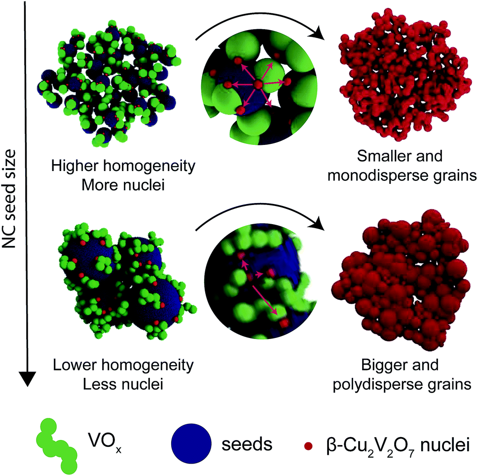 | ||
| Fig. 5 Schematic illustration of the growth process of β-Cu2V2O7. | ||
Taking advantage of the tunability afforded by the NC-seeded synthesis, the dependence of the photoelectrochemical (PEC) behavior on the grain size of the β-Cu2V2O7 films was investigated. The results are shown in Fig. 6. The optical properties of the films (Fig. S10†) were consistent with literature data for copper vanadates. The photocurrent density (J) versus the applied potential (E) of films synthesized from 6 nm, 11 nm, 14 nm and 40 nm NC seeds were collected in the presence of 0.1 M sodium sulfite (Na2SO3), which served as a hole scavenger, under simulated sunlight (Fig. S11†). The fast oxidation kinetics of Na2SO3 enables the study of the photoelectrochemical properties of β-Cu2V2O7 independently of their slow kinetic properties towards water oxidation.18,21 It must be noted that high dark currents were measured in the presence of sodium sulfite (Fig. S11†), which is in agreement with many other literature reports.18–20,22,23 While their origin remains to be investigated, they might be indicative of a dark electrochemical reaction occurring between the photoanode surface and the hole scavenger. The incident photon-to-current efficiency (IPCE) and the absorbed photon-to-current efficiency (APCE) follow the trend of the J–E curves and evidence weak photoresponse for wavelengths >600 nm just above the indirect band gap (Fig. S12†). The onset potential around 0.72–0.74 V vs. RHE for all the samples (Fig. S13†) is consistent with the flat band potential of β-Cu2V2O7, which is presently reported to lie between 0.68 V and 0.77 V vs. RHE, and with literature results (0.75 V vs. RHE).18,23Fig. 6 plots the net photocurrent density (Jnet = Jlight − Jdark) at 1.23 V vs. RHE versus the grain size and compares these results against the state-of-the-art values for β-Cu2V2O7.18,23 1.23 V vs. RHE was chosen as a reference voltage to ease the comparison with literature data. The photocurrent density at 1.23 V vs. RHE increases from 0.05 to 0.23 mA cm−2 as the grain size of β-Cu2V2O7 increases from 29 nm to 39 nm. In addition to the data points from the literature in Fig. 6, which refer to β-Cu2V2O7, numerous other crystalline phases of copper vanadates with grain sizes above 200 nm show lower photocurrent values below 0.1 mA cm−2 at 1.23 V vs. RHE in the presence of a hole scavenger in a 9.2 pH borate buffer solution.18–20,22,23 In the present work, the highest photocurrent density of 0.23 mA cm−2 at 1.23 V vs. RHE is achieved when the grain size is 39 nm which is exactly in the range of the estimated hole diffusion length of copper vanadates (20–40 nm).22 The films with smaller grains exhibit higher densities of grain boundaries, which are deleterious for the transport of electrons to the back contact. As the grain size increases, electronic transport improves, and thus the photocurrent increases up to the grain size of 39 nm. When the grain size becomes bigger than the charge carrier diffusion length, the photoexcited holes do not survive long enough to reach the electrolyte interface thereby drastically reducing the photocurrent density due to bulk recombination. It is interesting to note that the samples containing the interface β-Cu2V2O7/CuV2O6 exhibit a much higher photocurrent (0.43 mA cm−2 at 1.23 V vs. RHE) with respect to the pure phase samples. The bulk band gap alignment suggests that charge transfer from β-Cu2V2O7 to CuV2O6 is possible, and thus this could favor charge extraction thereby mitigating recombination.18
 | ||
| Fig. 6 Net photocurrent density (Jlight − Jdark) at 1.23 V vs. RHE measured in a 0.1 M sodium borate buffer (pH 8.2) containing 0.1 M Na2SO3 as a hole scavenger versus the β-Cu2V2O7 grain size. The black and blue colored data points are adapted from Guo et al.18 and Jiang et al.23Lh indicates the hole diffusion length of β-Cu2V2O7.22 | ||
Fig. 7 shows representative high resolution TEM (HR-TEM) images of the pure phase β-Cu2V2O7 and of the mixed phase β-Cu2V2O7/CuV2O6 along with the fast Fourier transforms (FFTs). The morphology of the two samples is very similar and the grain sizes are in the same size range found by XRD. The FFT analysis, carefully performed on multiple areas of the sample, has evidenced the simultaneous presence of β-Cu2V2O7 and CuV2O6 with a uniform spatial distribution rather than segregated in different domains. Such an intimate intermixing, which allows for an extended interface area, has been previously demonstrated to be advantageous for maximizing charge separation, and thus photoelectrochemical performance, in heterostructured nanocomposite electrodes.33
 | ||
| Fig. 7 HR-TEM along with the FFTs of (A) one sample of the pure phase β-Cu2V2O7, synthesized from 6 nm Cu NC seeds and (B) one sample of the mixed phase β-Cu2V2O7/CuV2O6, synthesized from 60 nm Cu NC seeds. | ||
Conclusions
To conclude, our findings reveal the unique opportunities offered by NC-seeded synthesis in materials chemistry. The reaction of Cu NC seeds with the molecular vanadium precursor VO(acac)2 results in the formation of copper vanadate thin films with tunable grain size. The diameter of the NC seeds plays a key role in determining the grain size and composition of the final reaction product. In situ XRD studies reveal the occurrence of a solid-state reaction between the seeds and the vanadium matrix formed during the annealing. The tunability of the grain size afforded by the NC-seeded synthesis offers a mean to study the dependence of the photoelectrochemical performance on the grain size in a range close to the charge carrier diffusion length of β-Cu2V2O7 (20–40 nm), something which has been not possible to date. A strong relationship between the grain size and the photocurrent density is revealed, the performance being maximized when the grain size is in the order of the charge carrier diffusion length for this material. Thus, the ability to tune the grain size with high precision is demonstrated to be of paramount importance for the rational design of novel photoabsorbers.Furthermore, the higher photoelectrochemical performance of the mixed phase samples β-Cu2V2O7/CuV2O6 suggests that nanostructuring plus hetero-structuring might be key to approach the theoretical performance of copper vanadate photoanodes.18,24,33 Future transient absorption measurements will be used to elucidate the correlation between size- and composition-dependent charge carrier dynamics and PEC performance.
Overall, this work demonstrates the potential of NC seeded synthesis to achieve structural and compositional tunability often inaccessible by other methods. This newly defined space in chemical reactivities, which links the more classical sol–gel and solid-state approaches, can be easily explored within the vast family of metal oxides targeting numerous different applications.1–12
Conflicts of interest
There are no conflicts to declare.Acknowledgements
This work was supported by the Swiss National Science Foundation (AP Energy Grant, project number PYAPP2_166897/1). M.S. acknowledges the H2020-Marie Curie Individual Fellowship with grant agreement number 753124. A. L. acknowledges the H2020-Marie Curie Individual Fellowship with grant agreement number 701745. Dr Mariateresa Scarongella is acknowledged for the transmission spectra in the ESI. Mr. Pranit Iyengar is acknowledged for providing one sample of the Cu nanocrystals. We thank Dr. Nestor Guijarro and Dr. Florian Le Formal in the group of Professor Kevin Sivula for assistance in the acquisition of the IPCE data reported in the ESI.†Notes and references
- J. W. Choi and D. Aurbach, Nat. Rev. Mater., 2016, 1, 16013 CrossRef.
- I. Bretos, R. Jiménez, J. Ricote and M. L. Calzada, Chem. Soc. Rev., 2018, 47, 291–308 RSC.
- B. Zhang, X. Zheng, O. Voznyy, R. Comin, M. Bajdich, M. García-Melchor, L. Han, J. Xu, M. Liu, L. Zheng, F. P. García de Arquer, C. T. Dinh, F. Fan, M. Yuan, E. Yassitepe, N. Chen, T. Regier, P. Liu, Y. Li, P. De Luna, A. Janmohamed, H. L. Xin, H. Yang, A. Vojvodic and E. H. Sargent, Science, 2016, 352, 333–337 CrossRef PubMed.
- R. D. L. Smith, M. S. Prévot, R. D. Fagan, Z. Zhang, P. A. Sedach, M. K. J. Siu, S. Trudel and C. P. Berlinguette, Science, 2013, 340, 60–63 CrossRef PubMed.
- I. Bretos, R. Jiménez, A. Wu, A. I. Kingon, P. M. Vilarinho and M. L. Calzada, Adv. Mater., 2014, 26, 1405–1409 CrossRef PubMed.
- T. Minegishi, N. Nishimura, J. Kubota and K. Domen, Chem. Sci., 2013, 4, 1120 RSC.
- K. Sivula and R. Van De Krol, Nat. Rev. Mater., 2016, 1, 15010 CrossRef.
- A. Agrawal, R. W. Johns and D. J. Milliron, Annu. Rev. Mater. Res., 2017, 47, 1–31 CrossRef.
- K. Lee, B. M. Tienes, M. B. Wilker, K. J. Schnitzenbaumer and G. Dukovic, Nano Lett., 2012, 12, 3268–3272 CrossRef PubMed.
- C.-H. Chuang, Y.-G. Lu, K. Lee, J. Ciston and G. Dukovic, J. Am. Chem. Soc., 2015, 137, 6452–6455 CrossRef PubMed.
- K. Lee, Y.-G. Lu, C.-H. Chuang, J. Ciston and G. Dukovic, J. Mater. Chem. A, 2016, 4, 2927–2935 Search PubMed.
- P. Tongying, Y.-G. Lu, L. M. G. Hall, K. Lee, M. Sulima, J. Ciston and G. Dukovic, ACS Nano, 2017, 11, 8401–8412 CrossRef PubMed.
- A. Loiudice, J. Ma, W. S. Drisdell, T. M. Mattox, J. K. Cooper, T. Thao, C. Giannini, J. Yano, L.-W. Wang, I. D. Sharp and R. Buonsanti, Adv. Mater., 2015, 27, 6733–6740 CrossRef PubMed.
- Q. Yan, J. Yu, S. K. Suram, L. Zhou, A. Shinde, P. F. Newhouse, W. Chen, G. Li, K. A. Persson, J. M. Gregoire and J. B. Neaton, Proc. Natl. Acad. Sci. U. S. A., 2017, 114, 3040–3043 CrossRef PubMed.
- D. de Waal and C. Hutter, Mater. Res. Bull., 1994, 29, 843–849 CrossRef.
- P. P. Sahoo, B. Zoellner and P. A. Maggard, J. Mater. Chem. A, 2015, 3, 4501–4509 Search PubMed.
- P. F. Newhouse, D. A. Boyd, A. Shinde, D. Guevarra, L. Zhou, E. Soedarmadji, G. Li, J. B. Neaton and J. M. Gregoire, J. Mater. Chem. A, 2016, 4, 7483–7494 Search PubMed.
- W. Guo, W. D. Chemelewski, O. Mabayoje, P. Xiao, Y. Zhang and C. B. Mullins, J. Phys. Chem. C, 2015, 119, 27220–27227 Search PubMed.
- J. A. Seabold and N. R. Neale, Chem. Mater., 2015, 27, 1005–1013 CrossRef.
- M. A. Lumley and K. S. Choi, Chem. Mater., 2017, 29, 9472–9479 CrossRef.
- L. Zhou, Q. Yan, A. Shinde, D. Guevarra, P. F. Newhouse, N. Becerra-Stasiewicz, S. M. Chatman, J. A. Haber, J. B. Neaton and J. M. Gregoire, Adv. Energy Mater., 2015, 5, 1500968 CrossRef.
- C.-M. Jiang, M. Farmand, C. H. Wu, Y.-S. Liu, J. Guo, W. S. Drisdell, J. K. Cooper and I. D. Sharp, Chem. Mater., 2017, 29, 3334–3345 CrossRef.
- C.-M. Jiang, G. Segev, L. H. Hess, G. Liu, G. Zaborski, F. M. Toma, J. K. Cooper and I. D. Sharp, ACS Appl. Mater. Interfaces, 2018, 10, 10627–10633 Search PubMed.
- M. Kim, B. Joshi, H. Yoon, T. Y. Ohm, K. Kim, S. S. Al-Deyab and S. S. Yoon, J. Alloys Compd., 2017, 708, 444–450 CrossRef.
- I. Khan and A. Qurashi, Sci. Rep., 2017, 7, 14370 CrossRef PubMed.
- T. W. Kim and K.-S. Choi, Science, 2014, 343, 990–994 CrossRef PubMed.
- D. Kang, T. W. Kim, S. R. Kubota, A. C. Cardiel, H. G. Cha and K.-S. Choi, Chem. Rev., 2015, 115, 12839–12887 CrossRef PubMed.
- L.-I. Hung, C.-K. Tsung, W. Huang and P. Yang, Adv. Mater., 2010, 22, 1910–1914 CrossRef PubMed.
- S.-C. Lu, M.-C. Hsiao, M. Yorulmaz, L.-Y. Wang, P.-Y. Yang, S. Link, W.-S. Chang and H.-Y. Tuan, Chem. Mater., 2015, 27, 8185–8188 CrossRef.
- E. L. Rosen, R. Buonsanti, A. Llordes, A. M. Sawvel, D. J. Milliron and B. A. Helms, Angew. Chem., Int. Ed., 2012, 51, 684–689 CrossRef PubMed.
- C. K. Kwok and S. B. Desu, J. Mater. Res., 1993, 8, 339–344 CrossRef.
- G. M. Clark and R. Garlick, J. Inorg. Nucl. Chem., 1978, 40, 1347–1349 CrossRef.
- A. Loiudice, J. K. Cooper, L. H. Hess, T. M. Mattox, I. D. Sharp and R. Buonsanti, Nano Lett., 2015, 15, 7347–7354 CrossRef PubMed.
Footnote |
| † Electronic supplementary information (ESI) available: Details of the Cu NC synthesis procedure, ligand stripping procedure, sample preparation methods, and experimental details for SEM, TEM, TGA, Raman spectroscopy, in situ and ex situ XRD, UV-Vis spectroscopy, FTIR spectroscopy and PEC measurements. See DOI: 10.1039/c8sc01314d |
| This journal is © The Royal Society of Chemistry 2018 |