
 Open Access Article
 This Open Access Article is licensed under a Creative Commons Attribution-Non Commercial 3.0 Unported Licence
Sustainable p-type copper selenide solar material with ultra-large absorption coefficient†
Erica M.
Chen
 a,
Logan
Williams
a,
Alan
Olvera
a,
Cheng
Zhang
b,
Mingfei
Zhang
a,
Guangsha
Shi
a,
John T.
Heron
a,
Liang
Qi
a,
L. Jay
Guo
b,
Emmanouil
Kioupakis
a and
Pierre F. P.
Poudeu
*a
a,
Logan
Williams
a,
Alan
Olvera
a,
Cheng
Zhang
b,
Mingfei
Zhang
a,
Guangsha
Shi
a,
John T.
Heron
a,
Liang
Qi
a,
L. Jay
Guo
b,
Emmanouil
Kioupakis
a and
Pierre F. P.
Poudeu
*a
aDepartment of Materials Science and Engineering, University of Michigan, Ann Arbor, 48109, USA. E-mail: ppoudeup@umich.edu
bDepartment of Electrical Engineering and Computer Science, University of Michigan, Ann Arbor, 48109, USA
First published on 15th May 2018
Abstract
Earth-abundant solar absorber materials with large optical absorption coefficients in the visible enable the fabrication of low-cost high-efficiency single and multi-junction thin-film solar cells. Here, we report a new p-type semiconductor, Cu4TiSe4 (CTSe), featuring indirect (1.15 eV) and direct (1.34 eV) band gaps in the optimal range for solar absorber materials. CTSe crystallizes in a new noncentrosymmetric cubic structure (space group F![[4 with combining macron]](https://www.rsc.org/images/entities/char_0034_0304.gif) 3c) in which CuSe4 tetrahedra share edges and corners to form octahedral anionic clusters, [Cu4Se4]4−, which in turn share corners to build the three-dimensional framework, with Ti4+ ions located at tetrahedral interstices within the channels. The unique crystal structure and the Ti 3d orbital character of the conduction band of CTSe give rise to near-optimal band gap values and ultra-large absorption coefficients (larger than 105 cm−1) throughout the visible range, which are promising for scalable low-cost high-efficiency CTSe-based thin-film solar cells.
3c) in which CuSe4 tetrahedra share edges and corners to form octahedral anionic clusters, [Cu4Se4]4−, which in turn share corners to build the three-dimensional framework, with Ti4+ ions located at tetrahedral interstices within the channels. The unique crystal structure and the Ti 3d orbital character of the conduction band of CTSe give rise to near-optimal band gap values and ultra-large absorption coefficients (larger than 105 cm−1) throughout the visible range, which are promising for scalable low-cost high-efficiency CTSe-based thin-film solar cells.
Introduction
Solar-cell research has focused on the development of low-cost highly efficient absorber materials. Recently popular materials include metal-halide perovskites, organic–inorganic hybrid perovskites,1 and copper metal chalcogenides (CMC) such as CuInSe2 (CIS)2 and CuIn1−xGaxSe2 (CIGS).3–5 The large absorption coefficient of these materials, coupled with the ability to engineer their band gap by chemical substitution, enable the realization of solar cells with power conversion efficiencies exceeding 20%.2–4,6,7 Although the efficiencies remain inferior to that of single-junction devices based on bulk crystalline silicon (25.6%),8,9 and thin-film GaAs (28.8%),10 the ability of perovskite- and CMC-based materials to be readily solution processed to solar cells11–14 provides a cost advantage that could pave the way to terawatt-scale deployment of photovoltaic technologies. Despite the promise of these material systems, the thermal instability of hybrid perovskites, the restrictions on the use of heavy metals (Cd, Pb, etc.), and the limited global supply of indium are roadblocks to the large-scale deployment of the existing leading perovskites and chalcogenide-based technologies. To address these issues, Earth-abundant copper-metal chalcogenides such as kesterites, Cu2SnZn(S,Se)4 (CZTS), obtained through chemical substitution of In3+ atoms in CuIn(S,Se)2 by Zn2+ and Sn4+, have been investigated.14,15 However, the efficiencies of devices based on these materials remain around 12.6% due to relatively low absorption coefficients, compared to CIGS, and unavoidable anti-site defects such as CuZn and ZnCu.16–19 Therefore, it appears that achieving low-cost, Earth-abundant copper metal chalcogenide solar cells with high efficiency requires the development of new chemical compositions and crystal structures rather than incremental variations of the chemistry of existing structures. Here, we report the discovery of a new ternary Earth-abundant CMC, Cu4TiSe4, copper titanium selenide (CTSe), and demonstrate its potential as a promising light-absorber for ultra-thin low-cost high-efficiency solar cells.Experimental section
Synthesis
High purity elemental powders of copper (99.5%, Alfa Aesar), titanium (99.5%, Alfa Aesar) and selenium (99.5%, Sigma Aldrich) were weighed out in a stoichiometric ratio and thoroughly ground under argon atmosphere using an agate mortar and pestle. The mixture was then flame-sealed in an evacuated (∼10−3 Torr) quartz tube and placed in the furnace. The furnace temperature was first ramped to 300 °C over 10 hours and held steady for 24 hours to allow the selenium to react with the rest of the elements. Then the temperature was increased to 550 °C for 120 hours and then the ampoules were cooled to room temperature over 24 hours. To improve the crystallinity of the synthesized materials, the samples were opened in an argon glove box, reground in an agate mortar and pestle and then resealed in quartz ampoules for annealing at 550 °C for 5 days. Single crystals suitable for X-ray structure determination were obtained by annealing a small amount of the sintered polycrystalline powder at 800 °C for 10 days.Thin film fabrication
First, a one-inch diameter and three-eighths inch thick target was produced by cold pressing and annealing the as-synthesized CTSe powder. The powder was loaded into a steel die between two sheets of Grafoil and consolidated under ambient atmosphere and an applied pressure of 395 MPa using a uniaxial hydraulic press. The target was subsequently annealed at 300 °C for 8 hours in a vacuum furnace. After cooling to room temperature, surface of the target was polished to matte finished using SiC paper. The resulting CTSe target was subsequently used for the fabrication of CTSe film using pulse laser deposition (PLD). The thin film was grown on a 500 μm Si substrate coated with 300 nm thermal oxide. The substrate was loaded into a Thermionics deposition chamber and a base pressure of ∼10−8 mbar was achieved. Argon was flowed in order to raise the chamber pressure to 7.4 × 10⁻² mbar, and then the substrate was heated to 500 °C at a rate of 20 °C per minute. The target was pre-ablated with 300 shots at 2 Hz with KrF exciplex laser applying an average fluence of 2.6 J cm−2. CTSe thin film growth was achieved by applying 6000 shots at 5 Hz to the target. The structure and microstructure of the deposited film was characterized through optical microscopy; SEM; and XRD measurements.Crystal structure determination
A single crystal of CTSe, with approximate dimensions 0.05 × 0.05 × 0.05 mm3 obtained from the high temperature annealing step was mounted on the tip of a glass fiber using epoxy glue. Intensity data were collected at 300 K on a STOE IPDS-2T diffractometer using a graphite-monochromated Mo-Kα radiation (λ = 0.71073 Å). The intensity data was indexed in the face centered cubic (fcc) Bravais lattice with unit cell parameter a = 11.2936(2) Å, and eight formula units per unit cell (Z = 8). The structure solution was obtained by direct methods in the space group F3c (no. 219) and refined by full-matrix least-squares techniques using the SHELXTL software package.20,21 The asymmetric unit cell contains three crystallographically independent metal positions M1 (24d), M2 (8a) and M3 (8b) and one Se atom position (32e). In the initial refinement cycle, Cu atoms were located at 24d (Cu1) and 8b (Cu2) sites with Ti occupying the 8a site. The refinement of this model resulted in R1 = 7.5%. However, the atomic displacement parameter of Ti was four times larger than that of Cu1 and Cu2. By exchanging the position of Cu2 (8a) and Ti (8b) atoms, the electroneutrality of the compound is maintained and the refinement of this model yielded R1 = 5.1% with the atomic displacement parameter of Ti dropping by 50%. In the final refinement iteration, secondary extinction correction and anisotropic displacement parameters were included for all atoms. This resulted in a final R1 ∼ 4%. The final charge-balanced composition of the crystal obtained from the refinement was (Cu+)4(Ti4+)(Se2−)4. The assigned oxidation states of Cu and Ti atoms were also confirmed by bond valence sum (BVS) calculations. Additional details on the structure refinement and summary of crystallographic data are given in Table S1.† Table S2† provides atomic coordinates and isotropic displacement parameters of all atoms and Table S3† summarizes selected inter-atomic distances. The graphical representation of the crystal structure was created using the graphical software Diamond22 with ellipsoid representations (98% probability level) for all atoms. Detailed crystallographic data can be obtained from Fachinformationszentrum Karlsruhe, 76344 Eggenstein-Leopoldshafen, Germany, Fax: +49-7247-808-666; E-mail: E-mail: crysdata@fiz.karlsruhe.de, on quoting the depository number CSD-432569.†
Structural characterization
To assess the phase purity and structure of the as-synthesized bulk polycrystalline powder and the PLD fabricated thin-films of CTSe, X-ray diffraction patterns were recorded and compared to the theoretical pattern of CTSe calculated using single crystal structure data (Fig. S1 and S2†). The powder patterns for the bulk powder samples were collected in reflection geometry on a Rigaku Miniflex 600 powder diffractometer operating under 40 kV and 15 mA using a monochromated Cu-Kα radiation (λ = 1.5418 Å). XRD patterns for the films grown on SiOx/Si substrate were recorded on a rotating anode Rigaku Rotoflex operating at 40 kV and 100 mA. As can be seen from Fig. S2a,† there is an excellent match in both the position and relative intensity of various peaks observed on the experimental diffraction of the as-synthesized polycrystalline CTSe powder and the simulated powder diffraction pattern calculated using single-crystal data. This suggests successful large-scale synthesis of bulk polycrystalline powder of CTSe as single-phase. The phase purity of the synthesized CTSe polycrystalline powder was also confirmed through measurement of the true density using He gas pycnometry (Quantachrome Ultrapyc 1200e MUPY-30 pycnometer). Hand pressed pellets of CTSe was loaded into the sample chamber with known volume and He gas was used to flow purge and pressurize the chamber to 15 psi. The volume of CTSe extracted from this measurement along with the sample weight enabled the calculation of the true density, which was found to be 5.77(6) g cm−3. This value is comparable, within the instrument precision of 5%, to the theoretical density of 5.69(8) g cm−3, confirming the single-phase nature of the synthesized CTSe polycrystalline powder.A comparison of the diffraction pattern obtained from the PLD deposited thin-film of CTSe (Fig. S2a†) with the diffraction patterns of bare substrate and the theoretical pattern from single crystal data suggests successful formation of CTSe thin-film using PLD technique. All diffraction peaks from CTSe thin film can be associated to peaks from the bare substrate (thermal oxide + silicon) and high intensity peaks from the theoretical pattern of CTSe. Careful comparison of the relative intensity of the observed (222) and (044) peaks from the XRD pattern of CTSe thin film to the corresponding peaks on the theoretical pattern of CTSe revealed a preferential growth along (222) plane. The microstructure of the PLD deposited film was also examined using scanning electron microscopy (SEM). SEM analysis was performed using a Philips XL-30 with a tungsten filament and operating at 20 keV. The deposited CTSe thin film consists of densely packed prismatic grains with uniform particle size of approximately 70 nm (Fig. S2b†).
Chemical analysis
The chemical composition of the synthesized powder of CTSe was determined using wavelength dispersive X-ray fluorescence (XRF) spectroscopy. Polycrystalline powder of CTSe was suspended onto Chemplex XRF cup with 0.3 μm thick Prolene film. The specimen was loaded into a Rigaku Supermini 200 equipped and data collections were performed using Pd source (operating at 50 kV, 200 W) under helium gas. The resulting composition in atomic percent is Cu (45.9%), Se (43.7%) and Ti (10.4%), which is comparable to the nominal atomic percentages of 44%, 44% and 11% for Cu, Se, and Ti, respectively. Similar composition (within the precision of the respective techniques) was obtained from the energy dispersive spectroscopy (EDS) analysis of hot pressed pellet of the synthesized materials used as target for the fabrication of CTSe thin film using pulse laser deposition technique. EDS analysis of the target performed using scanning electron microscope (SEM, FEI Nova Nanolab) confirmed the chemical composition of the target as Cu (47.8% ± 0.7%); Ti (10.5% ± 0.1%); Se (41.7% ± 0.6%), which is consistent with the composition of the starting polycrystalline powder sample. The stoichiometry of the deposited film was also determined by EDS analysis and the measured atomic composition of Ti (11% ± 0.5), Cu (41% ± 3) and Se (48% ± 3) is consistent with the composition of the starting target.Differential scanning calorimetry
The thermal stability and phase purity of the synthesized polycrystalline powder of CTSe was probed using differential scanning calorimetry (DSC). Approximately 30 mg of finely ground polycrystalline powder were sealed inside a small quartz tube (2 mm × 3 mm) under a residual pressure of 10−3 Torr. A sealed blank quartz tube was used as the reference. The measurement was performed from room temperature to 850 °C in two heating and cooling cycles under flowing nitrogen gas. Heating and cooling curves on both cycles showed a single endothermic thermal event at 820 °C and a single exothermic event as the same temperature, indicating a congruent melting and crystallization of the compound (Fig. S2b†). In addition, the similarity of the DSC curves in both heating and cooling cycles confirmed the thermal stability of the structure.DFT phonon dispersion, structure stability and elastic constants
Density functional theory (DFT) calculations were performed with the Vienna ab initio simulation package (VASP)23 within the projector augmented wave (PAW) formalism.24,25 For the exchange–correlation functional we employed the generalized gradient approximation (GGA) as parameterized by Perdew, Burke, and Ernzerhof (PBE).26 For the sampling of the Brillouin zone we employed the Monkhorst–Pack scheme with a grid of 15 × 15 × 15 for CTSe supercell.27 The cut-off energy for the plane wave basis was 400 eV, and the convergence criterion for the electron-density self-consistency cycles was 10−6 eV. Three independent elastic constants C11, C12 and C44 of CTSe cubic crystal structure were calculated based the derivatives of the total energy as functions of the specially designed strain.28 The phonon dispersion relation of CTSe (Fig. S3†) was determined along high symmetry k-points path in the Brillouin zone using the Phonopy package29 based on the force constants obtained from VASP calculations. The phonon frequencies are positive throughout the Brillouin zone, validating the dynamic stability of the material. Therefore, CTSe should be stable under any small inhomogeneous deformation inside its crystal structure.Electronic band structure and optical absorption calculations
Density functional and many-body perturbation theory calculations for the band structure and optical properties were performed using the Vienna Ab initio Simulation Package (VASP).23,25,30–32 The GW series of Projector Augmented Wave (PAW) pseudopotentials was used.25,33 Valence electrons 11, 12, and 6 were included for Cu, Ti, and Se respectively. Forces on all atoms were relaxed to under 0.005 eV Å−1. The plane wave basis set cutoff was set at 700 eV. The electronic convergence criterion was set at 10−8 eV. Multiple levels of theory were used. The hybrid functional of Heyd, Scuseria, and Ernzerhof (HSE06)34,35 was used to relax the crystal structure and to obtain the starting point for subsequent many-body perturbation theory calculations. Quasi-particle (QP) corrections based on the GW method (G0W0)36 along with the maximally localized Wannier function method as implemented in the Wannier90 code37 were used to determine the quasiparticle band structure throughout the Brillouin zone. The dielectric functions and the optical absorption coefficient were obtained with the Bethe–Salpeter equation (BSE) method.38,39 Gamma-centered grids of 4 × 4 × 4 k points were used for all calculations. Convergence parameters of 1440 bands, a 300 eV GW basis set energy cutoff, and a value of 200 for NOMEGA were used in G0W0 calculations. BSE calculations included 32 occupied and 28 unoccupied bands.Ellipsometry measurement of reflective index (n) and extinction coefficient (k)
A spectroscopic ellipsometer (J.A. Woollam Co. M-2000) is used to measure the index of refraction (n) and the extinction coefficient (k) of CTSe thin film. The measurement was carried out at three incident angles of 55°, 65°, and 75°. The ellipsometer measures the amplitude and phase difference of the s- and p-polarized light after their reflection off the sample. Afterwards, an inverse calculation was done in order to extract the optical properties of the film. Since the deposited CTSe film is thin and semi-transparent in certain wavelength ranges, the incident light will penetrate through the film and reach the Si substrate. In order to separate the effect of light absorption by the Si substrate, and accurately determine the refractive index of the deposited CTSe thin-film, a thin layer (∼300 nm) of thermal oxide was first deposited on the Si substrate prior to the CTSe film deposition. The additional thermal oxide layer facilitates the decoupling of either film thickness or absorption coefficient contributions to Ψ and Δ, by providing additional reflected light, and thus, additional information for an accurate evaluation of the refractive index and thickness of the CTSe film during the ellipsometry data fitting process (interference enhancement method).40,41 The ellipsometry data was fitted with a B-spline model that takes into account the Kramers–Kronig relation. This experimental setup and modeling determine the quantities n, k and the film thickness. The index of refraction n and the extinction coefficient k are shown in Fig. S4.†Determination of absorption coefficient and optical band gap
Using the extinction coefficient (k) determined from the fitting of the spectroscopic ellipsometry data (Fig. S4†), we are able to calculate the absorption coefficient using the expression α = 4πk/λ = 10![[thin space (1/6-em)]](https://www.rsc.org/images/entities/char_2009.gif) 135462Ek, where α is the absorption coefficient in inverse meters, k is the extinction coefficient, and E is energy in eV. The absorption coefficient is then used for Tauc analysis42 using the equation y = (αhν)1/r, where h is Planck's constant, ν is frequency and r is a constant (r = 2 for allowed indirect transition and r = 1/2 for direct allowed transition). Fitting the linear portion of the transformed absorption coefficient vs. energy curve enabled determination of both direct and indirect bang gap as the linear regression's x intercept as shown in Fig. S5a and b.†
135462Ek, where α is the absorption coefficient in inverse meters, k is the extinction coefficient, and E is energy in eV. The absorption coefficient is then used for Tauc analysis42 using the equation y = (αhν)1/r, where h is Planck's constant, ν is frequency and r is a constant (r = 2 for allowed indirect transition and r = 1/2 for direct allowed transition). Fitting the linear portion of the transformed absorption coefficient vs. energy curve enabled determination of both direct and indirect bang gap as the linear regression's x intercept as shown in Fig. S5a and b.†
Estimated photovoltaic conversion efficiency (EPCE)
The upper limit of the estimated photovoltaic conversion efficiency (EPCE) as a function of thickness of the absorber layer was calculated according to a modified version of the Shockley–Queisser limit as shown in Fig. 5.43 The impedance matching factor, or fill factor, and the ratio of open circuit voltage to band gap voltage were left constant at the values expected for full absorption of light into the materials, as tabulated by Rühle.44 The spectrum losses were modified to account for the fraction of light that would be absorbed for a given thickness, using material absorption coefficients that were interpolated throughout the energy range specified in the AM1.5G solar spectrum.45 Due to incomplete data, for CdTe, the absorption coefficient from 4.145 eV to 4.429 eV was assumed to remain constant at the 4.145 eV value; this region of the solar spectrum has a negligible effect on the final result due to the small phonon flux in this region and the relatively high absorption coefficients in this region compared to the 1–3 eV range.Electronic transport measurement
Specimens for simultaneous measurement of the thermopower and electrical conductivity were fabricated by pressing polycrystalline CTSe powder with a uniaxial hot press using graphite dies and plungers. 100 MPa of pressure was applied with the hydraulic system and the furnace shell was evacuated and flushed with argon several times before maintain a constant 20 L min−1 flow of argon for the remainder of the pressing time. The furnace temperature was increased to 450 °C at a scan rate of 200 °C h−1, dwelled for 4 hours and finally ramped down to room temperature at 100 °C h−1. rectangular bars specimen, ∼2.0 × 2.1 × 9.5 mm, were cut from the pressed pellets using a wire saw and SiC slurry, then polished to mirror finished using SiC papers. The thermopower and the electrical resistivity were measured simultaneously from room temperature to 525 °C using an ULVAC-RIKO ZEM-3 apparatus. The instrument's precision on the electrical resistivity and the Seebeck coefficient data is ±4%. CTSe exhibits p-type semiconducting behavior as indicated by the positive values of the thermopower and the nearly exponential increase in the electrical conductivity with increasing temperature (Fig. S6†). The thermopower rapidly increases from 30 μV K−1 at 300 K to 200 μV K−1 at 800 K. The electrical conductivity initially remains constant at 1 S cm−1 from 300 K to 450 K and thereafter slowly increase with rising temperature to 4 S cm−1 at 600 K. Beyond this temperature, the electrical conductivity drastically increase with further increase in temperature reaching 11 S cm−1 at 800 K.Results and discussion
Synthesis and structure
CTSe crystallizes in the noncentrosymmetric cubic space group F3c (no. 219) at ambient conditions with lattice parameter a = 11.2936 (2) Å and adopts a new structure type that can be regarded as a 2a × 2a × 2a superstructure of sulvanite (Cu3VS4)46 (Fig. 1a and b). Chemically, CTSe is an analog of CZTS where 2Cu+ and Ti4+ replace the six positive charges from Zn2+ and Sn4+ cations. Similarly to the zincblende-type structure of CIS, CIGS and CZTSSe, which features a characteristic 3D network of tetrahedrally coordinated metal atoms, MSe4, (M = Cu, Sn, In, Zn or Ga), Cu and Ti metal atoms in CTSe are also tetrahedrally coordinated by selenium. However, while metal tetrahedra in zincblende-type compounds share only corners to form the 3D network, CuSe4 tetrahedra (Cu(1)Se4 and Cu(2)Se4) in CTSe share both edges and corners in all directions to build a 3D framework of [Cu4Se4]4− anionic clusters (Fig. 1b). Within the [Cu4Se4]4− clusters, Cu(2)Se4 tetrahedra share all edges with Cu(1)Se4 tetrahedra, while Cu(1)Se4 tetrahedra exclusively share corners with each other (Fig. 1d–f). The resulting spatial arrangement of Cu(1)Se4 and Cu(2)Se4 tetrahedra is topologically equivalent to the sulvanite structure (with Cu(2)Se4 corresponding to VS4 and Cu(1)Se4 corresponding to CuS4). Using the [Cu4Se4]4− clusters as building units, the 3D structure of CTSe can simply be described as two interpenetrated face centered cubic (fcc) lattices in which Ti4+ atoms are located at tetrahedral interstices within the channels (Fig. 1b). This structural representation of CTSe, based on the Cu-centered [Cu6] octahedral cluster, Cu@[Cu]6, is also topologically similar to a double-perovskite structure. The TiSe4 tetrahedra in the structure of CTSe are isolated from each other and share only corners with Cu(1)Se4 and Cu(2)Se4 tetrahedra (Fig. 1d and f).
 | ||
| Fig. 1 Crystal structure of CTSe projected along [001]. (a) A ball-and-stick representation showing the 3D connectivity between metal tetrahedra, MSe4; (b) an alternate polyhedral representation highlighting octahedral building blocks of [Cu4Se4]4− anionic clusters. The [Cu4Se4]4− anionic clusters form two interpenetrated face centered cubic (fcc) lattices (yellow and purple denote the two sublattices) to generate a 3D structure that is topologically similar to a double perovskite, with Ti4+ ions located at tetrahedral sites within the channels; (c) [Cu4Se4]4− anionic cluster consisting of a Cu-centered hexanuclear octahedral [Cu]6 cluster capped by Se atoms on four of the eight triangular faces; (d) TiSe4 tetrahedron shares only corners with Cu(1)Se4 tetrahedra; (e) environment of Cu(1) and Cu(2) and their connectivity within the [Cu4Se4]4− anionic cluster. Cu(2)Se4 tetrahedron share all edges with Cu(1)Se4 tetrahedra, Cu(1)Se4 tetrahedra exclusively share corners with each other and Cu(2)Se4 tetrahedra are isolated from each other; (f) TiSe4 tetrahedron shares only corners with Cu(2)Se4 tetrahedra and TiSe4 tetrahedra are isolated from each other. | ||
The observed edge-sharing between Cu(1)Se4 and Cu(2)Se4 tetrahedra in the structure of CTSe (Fig. 1e) presumably results from the smaller fraction of structural vacancies in the compound when compared to zincblende structure. For example, a unit cell of CTSe is equivalent to eight unit cells (2 × 2 × 2 superstructure) of a fcc (faced centered cubic) lattice of Se atoms in which 5/8 of the tetrahedral sites (total of 40 tetrahedral sites per unit cell of CTSe) are occupied in an ordered fashion by Cu and Ti, whilst the remaining 3/8 (24 sites) are vacant. In an equivalent 2 × 2 × 2 superstructure of CuInSe2, the fcc lattice is formed by Se atoms with half (32 sites) of the available tetrahedral site occupy by Cu/In (50/50). The larger fraction of occupied tetrahedral sites in CTSe structure results in edge-sharing and corner-sharing tetrahedra, whereas only corner-sharing connectivity between tetrahedral is observed in zincblende structures. This difference in the fraction of occupied tetrahedral sites and connectivity between tetrahedra leads to a slightly higher density for CTSe (5.69 g cm−3) and higher structural stability when compared to cubic (sphalerite) CuInSe2 (5.57 g cm−3),47 which exhibits structural transition to higher density (5.77 g cm−3) low symmetry chalcopyrite structure at room temperature.48 The Cu–Se bond distances in CTSe range from 2.4328(2) Å for Cu(2)–Se to 2.4407(6) Å for Cu(1)–Se, which is comparable to the Cu–Se bond length of 2.435 Å observed in CuInSe2. The Ti–Se bond length of 2.4584(2) Å is 3.7% shorter than the bond distance of 2.553 Å reported in TiSe2.49 The unique composition and structural features of CTSe, compared to zincblende-type solar absorbers, give rise to extraordinary electronic and optical properties that were theoretically and experimentally investigated in this work.
Electronic structure
Band-structure calculations with hybrid density functional and many-body perturbation theory reveal that CTSe is an indirect-gap semiconductor with a 1.22 eV gap from M to Γ (Fig. 2a). However, the minimum direct gap (at M), which determines the onset of optical absorption, is slightly larger at 1.46 eV and close to the Shockley–Queisser optimal value.43 What makes CTSe particularly promising for solar cells, however, is the large density of states (DOS) near the band edges (Fig. 2b), which gives rise to optical absorption coefficients larger than 105 cm−1 throughout the visible range (Fig. 3). The large DOS derives from the flat valence (which consists of Cu 3d and Se 4p orbitals) and conduction (composed of Ti 3d states) bands. As a result of this unique band structure, CTSe is a superior absorber material for thin-film solar cells compared to GaAs, CIGS, and CZTS (which feature broad s-type conduction bands with a lower density of states), and CTSe thin-film solar cells reach comparable efficiencies at a much lower thickness. The calculated absorption coefficient of CTSe is compared to experiment and other absorber materials in Fig. 3. CTSe is predicted to outperform all established absorber materials in the 1.1–2.8 eV range that contains most of the terrestrial solar spectral irradiance.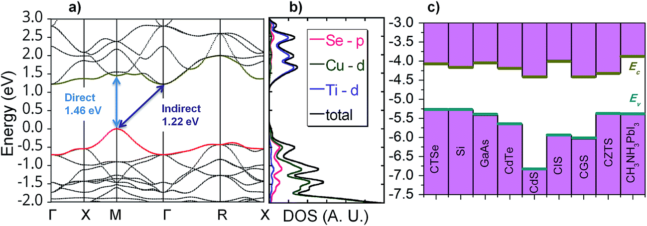 | ||
| Fig. 2 Electronic band structure of CTSe. (a) Calculated band structure highlighting the relatively flat valence (VB) and conduction (CB) bands, and the presence of both indirect (1.22 eV) and direct (1.46 eV) band gaps with similar values. (b) Projected density of states (DOS) highlighting the major orbital contributions; (c) band alignment of CTSe relative to vacuum and other photovoltaic materials. | ||
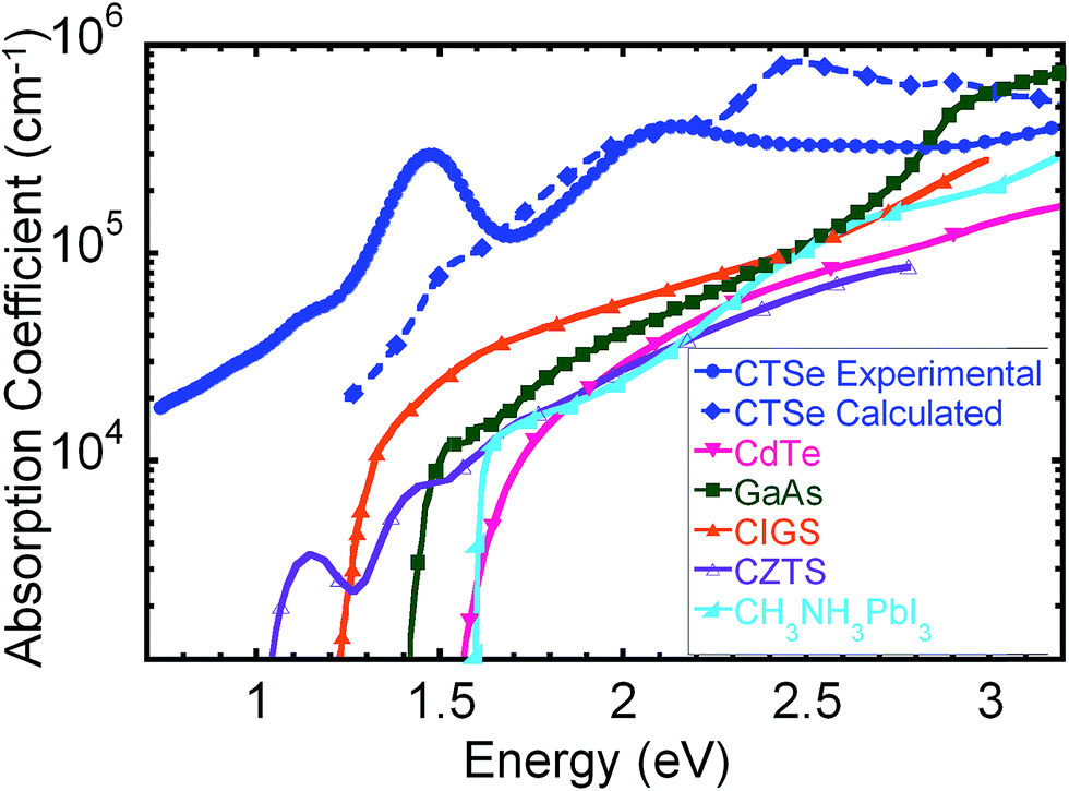 | ||
| Fig. 3 Theoretical and experimental absorption coefficients of CTSe compared to leading solar absorber materials such as CdTe,52 GaAs,53 CIGS,54 and CZTS,55 and CH3NH3PbI3.56 CTSe outperforms all established solar-absorber materials in the 1.1–2.8 eV range. | ||
Thermal and structural stability of CTSe
To probe the theoretically predicted electronic and optical properties of CTSe, polycrystalline powders were prepared through solid-state reaction of the elements at moderate temperatures (see ESI†). The excellent match, in both peak positions and intensity distributions, between the experimental X-ray powder diffraction pattern and the theoretical pattern generated using single crystal structure data confirms the single-phase nature of the as-synthesized polycrystalline powder (Fig. S1a†). In addition, the true density of the synthesized material measured using helium gas pycnometry was found to be 5.77(6) g cm−3, which is comparable, within the instrument precision of ±5%, to the theoretical value of 5.69(8) g cm−3 calculated from the crystal structure data further confirming the high purity of the synthesized material. Further confirmation of the single-phase nature of the synthesized CTSe, polycrystalline powders was obtained from differential scanning calorimetry (DSC) measurement. DSC curves recorded for two successive heating and cooling cycles show a single endothermic peak of melting at 850 °C on heating and a single exothermic peak of crystallization at 850 °C on cooling indicating a congruent melting and crystallization of the compound (Fig. S1b†). No sign of phase transition and decomposition of the sample were detected on the DSC curves suggesting a good thermal stability of the compound.To further investigate the structural stability of CTSe, we applied density functional theory (DFT) calculations (see ESI†) to determine (1) the formation energy, (2) the three independent cubic elastic constants (C11, C12 and C44), and (3) the phonon dispersion relation of CTSe. The formation energy of CTSe, based on the chemical reaction 2CuSe2 + 2Cu + Ti → Cu4TiSe4 is −3.03 eV per formula unit, which indicates a strongly exothermic reaction and suggests that CTSe is thermodynamically stable relative to CuSe2, Cu, and Ti. Moreover, the calculated elastic constants for CTSe are C11 = 90.75 GPa; C12 = 67 GPa; and C44 = 21.33 GPa, which satisfy the Born elastic stability criteria for a cubic structure at zero external pressure50 [(C11 − C12) > 0, C44 > 0, and (C11 + 2C12) > 0]. In addition, the phonon dispersion relation of CTSe (Fig. S3†) displays no imaginary frequencies, indicating the stability of CTSe with respect to spontaneous structural transformations by dynamic lattice vibrations.51 Therefore, the thermodynamic, elastic, and dynamic stability of CTSe, coupled with the congruent melting and crystallization observed from DSC curves, implies a relatively facile fabrication of crystalline CTSe thin films using various deposition methods, starting from high density targets of the synthesized polycrystalline powders.
Therefore, thin-films of CTSe on 300 nm SiOx/Si substrates were fabricated by pulsed laser deposition (PLD) in order to investigate their optical properties as well as the potential of CTSe as a solar material (see Experimental section for details on the deposition parameters). The structure and chemical composition of the films post deposition were confirmed by X-ray diffraction and scanning electron microscopy-energy dispersive X-ray spectroscopy (SEM-EDS) (Fig. 4 and S2†). Careful comparison of the X-ray diffraction patterns of CTSe thin films, with that of bare substrate and the calculated theoretical pattern of CTSe revealed that the X-ray diffraction pattern of the resultant thin film matches the substrate's pattern and includes the 3 major peaks ((222), (044) and (226)) from the CTSe phase. However, the CTSe peaks exhibit large differences in the relative intensity. The intensity of the (222) peak is larger (at least three times) than that of (044), which suggests that the film is polycrystalline with a strong orientation towards (222). SEM images reveal that the deposited CTSe films consist of finely aggregated polycrystalline particles (35–60 nm) with larger and thinner flakes that most likely result from “splashback” during the deposition process. The stoichiometry of the deposited film was confirmed by EDS analysis and is consistent with the composition of the target. The composition mapping of the films also reveals a uniform distribution of the elements (Fig. 4).
 | ||
| Fig. 4 SEM image and composition mapping of CTSe thin film. (a) Secondary electron image of the area. Qualitative EDS maps showing the distribution of (b) Cu, (c) Se and (d) Ti. | ||
Optical and electronic properties
The optical properties of the deposited films were characterized by the reflection-type spectroscopic ellipsometry from 200 nm to 1680 nm. The measured refractive index (n) and extinction coefficient (k) of CTSe (Fig. S4†) show a broadband absorption in the visible and near-infrared (near-IR) range and two strong absorption peaks around 650 nm and 900 nm, respectively. The absorption coefficient of CTSe calculated using the extinction coefficient from ellipsometry data is plotted in Fig. 3 and compared to our theoretical predictions and other materials. Both the predicted and the measured absorption coefficient of CTSe are larger than 105 cm−1 and far superior to the absorption coefficients of most traditional solar absorbers such as CdTe, GaAs, CIGS, CZTS, and Si within the range 1.1 eV to 2.8 eV, where most of the light in the terrestrial solar spectrum resides. Careful analysis of the absorption curves using Tauc fitting enables the determination of experimental indirect band gap of 1.15 eV and direct band gap of 1.34 eV (Fig. S5†). Interestingly, the direct band gap extracted from ellipsometry is very similar to the direct optical band gap of 1.31 eV derived from diffuse reflectance data on CTSe powder sample (Fig. S6†). These experimental values of the band gaps are comparable to the theoretically predicted indirect (1.22 eV) and direct (1.46 eV) band gaps of CTSe, and are well within the Shockley–Queisser range of optimal band gaps (1.1–1.5 eV). In addition, the indirect band gap of CTSe favors long minority-carrier lifetimes and precludes the re-emission of the absorbed photons and the need for photon recycling, in contrast to direct-gap solar absorbers such as GaAs. Moreover, the small energy difference (∼0.2 eV) between the direct and indirect gaps implies only a small additional energy loss due to carrier thermalization. These data offer the possibility of creating CTSe based solar cells of equal or superior efficiency to CdTe or GaAs cells at a fraction of the thickness. However, careful examination of the optical absorption curve from ellipsometry measurement on CTSe thin film (Fig. 3) as well as the diffuse reflectance data (Fig. S6†) measured on CTSe bulk powder sample revealed a tail below the sharp absorption peak. This likely indicates that the as-synthesized CTSe is doped with impurity states located within the band gap. Indeed, the Urbach tail analysis of the absorption curve revealed the presence of three linear regions with Urbach energies 135 meV, 297 meV, and 429 meV within the band gap of CTSe (Fig. S7†). The large values obtained for the Urbach energy point to large concentrations of defects existing within the band gap of CTSe. Our preliminary theoretical defect calculations indicated that the impurities arose from the formation of Cu vacancies such as VCu as well as antisite defects.Temperature dependent electronic transport measurement revealed that CTSe is a p-type semiconductor (Fig. S8†). The thermopower increases with temperature from 30 μV K−1 at 300 K to 200 μV K−1 at 800 K whereas the electrical conductivity increases from 1 S cm−1 at 300 K to 11 S cm−1 at 800 K. Interestingly, the temperature dependence of the electrical conductivity show two thermally activated electronic transitions around 400 K and 700 K. Fitting both transitions using the Arrhenius equation ln(σ) = ln(σ0) − Ea/KT (where Ea is the activation energy and K is the Boltzmann constant) leads to the activation energy of ∼140 meV for the transition at 400 K and an activation energy of ∼296 meV for the transition at 700 K (Fig. S9†). The observed activations energies are consistent with the Urbach energies calculated from the analysis of the tail of the optical absorption curve, further confirming the presence of localized electronic defects within the band gap of CTSe. Therefore, further work focusing on the reduction of the density of electronic defects within CTSe is needed to improve its potential as solar absorber material.
To quantify the advantages of CTSe for thin-film solar cells, we determined the upper limit of the estimated photovoltaic conversion efficiency (EPCE) as a function of absorber thickness and compared to that of GaAs, CdTe. The EPCE upper limit was calculated by evaluating the fraction of incident light absorbed for each wavelength in the AM1.5G solar spectrum, as determined by the absorption coefficient (Fig. 3), and by including the spectral losses in the Shockley–Queisser limit.43–45 The fill factor and the ratio of the open-circuit voltage to the band gap voltage were left at their full absorbance values for this analysis. As shown in Fig. 5, the estimated maximum efficiency of CTSe obtained using both the predicted and the measured absorption coefficients is significantly larger than that of GaAs and CdTe at low film thickness. This result is supported by the ultra-large absorption coefficient of CTSe throughout the 1.1–2.8 eV range, which enables higher efficiencies at approximately one order of magnitude lower film thickness compared to CdTe and GaAs. For instance, a maximum EPCE of 30% is anticipated for a 0.2 μm CTSe thin film compared to 5 μm GaAs film for similar EPCE value. This analysis suggests the potential for the production of high-efficiency and flexible CTSe-based solar cell devices at low cost, paving the way to sustainable large-scale deployment of lightweight, high-efficiency solar cells based on absorber materials from cheap and environmentally friendly elements.
 | ||
| Fig. 5 Estimated photovoltaic conversion efficiency (EPCE) as a function of thickness for CTSe compared to CdTe52 and GaAs.53 CTSe reaches an efficiency of 30% for a thickness of 200 nm, approximately one order of magnitude thinner than typical CdTe or GaAs devices (1.5–5 μm). | ||
The analysis of the band alignment of CTSe relative to other leading p-type solar absorber materials such as Si, GaAs, CdTe, CdS, CIS, CGS, CZTS and CH3NH3PbI3 is shown in Fig. 2c. The conduction band minimum (CBM) of CTSe is located 4.06 eV below the vacuum level and the valence band maximum (VBM) is located 5.28 eV below the vacuum level. This places the band edges very close to those of GaAs (−4.00 eV and −5.39 eV), CdTe (−4.18 eV and −5.66 eV) and CH3NH3PbI3 (−3.88 eV and −5.39 eV), a halide perovskite that is currently the focus of intense research efforts for solar cell applications.11 The similarity of the band-edge positions to established solar absorbers indicate that CTSe may be compatible with commercial solar-cell architectures and manufacturing technologies, which should accelerate the development of optimal CTSe-based devices. However, to achieve such working photovoltaic device based on CTSe, one must first reduce or eliminate the high density of defects (Cu vacancies) that contribute to absorption well below the band gap and therefore hamper the photoconductivity of the materials.
Concluding remarks
In summary, we discovered a new Earth-abundant ternary copper titanium selenide, CTSe, and assessed its potential as a promising solar absorber for low-cost, scalable, high-efficiency, single junction solar cells. CTSe adopts a new cubic structure type in which CuSe4 tetrahedra share both corners and edges to form a 3D framework topologically similar to double perovskite with isolated TiSe4 tetrahedra located within the channels. The unique structural feature of CTSe results in optimal theoretical/experimental band gaps of 1.22 eV/1.15 eV (indirect) and 1.46 eV/1.34 eV (direct), in the optimal range according to the Shockley–Queisser analysis. The Ti 3d orbital character of the conduction band results in ultra-large absorption coefficient (∼105 cm−1) throughout the visible, outperforming most traditional absorbers such as CZTS, CIGS, GaAs and CdTe in the 1.1–2.8 eV range. A CTSe material thickness of only 200 nm is needed to outperform GaAs and CdTe solar cells that are typically a few microns thick. In addition, CTSe was found to be stable from energetic, elastic and dynamic aspects, which significantly enhances the prospect of realizing scalable, low-cost, high- efficiency, lightweight, and environmentally friendly next generation solar cells.Author contributions
E. C. synthesized the samples, carried out structural characterization, fabricated CTSe thin-film, performed the SEM characterization, performed data analysis, and co-wrote the manuscript. A. O. helped with sample synthesis, performed structural characterization and data analysis, and co-edited the manuscript. L. W., G. S., and E. K. performed calculations for the electronic band structure, band gap, optical absorption coefficient, and the estimated photovoltaic conversion efficiency, performed data analysis and co-wrote the manuscript. C. Z. and J. G. performed optical property measurement, performed data analysis and co-edit the manuscript. M. Z. and L. Q. performed calculations of phonon dispersion, and elastic constants, performed data analysis and co-edit the manuscript. J. T. H. helped with thin-film fabrication, data analysis and co-edited the manuscript. P. F. P. P. conceived the experiment, performed crystal structure measurement, analyzed the results and co-wrote the manuscript.Conflicts of interest
The authors declare no competing financial interest.Acknowledgements
We gratefully acknowledge the financial support from the Department of Energy, Office of Basic Energy Science under Award # DE-SC-0008574 for materials synthesis, structural characterization, and fabrication of CTSe thin-film. The band structure and optical absorption calculations were supported by the National Science Foundation through grant number DMR 1561008, and used resources of the National Energy Research Scientific Computing Center, a DOE Office of Science User Facility supported by the Office of Science of the U.S. Department of Energy under Contract No. DE-AC02-05CH11231. This work made use of the SEMs (FEI Quanta3D and FEI Nova Nanolab) from the Michigan Materials Characterization Center, (MC)2, purchased with funds from the National Science Foundation Awards DMR-0315633 and DMR-0723032.References
- M. M. Lee, J. Teuscher, T. Miyasaka, T. N. Murakami and H. J. Snaith, Science, 2012, 338, 643–647 CrossRef PubMed.
- R. A. Joshi, V. S. Taur and R. Sharma, Mater. Res. Bull., 2012, 47, 2206–2211 CrossRef.
- P. Jackson, D. Hariskos, E. Lotter, S. Paetel, R. Wuerz, R. Menner, W. Wischmann and M. Powalla, Prog. Photovoltaics, 2011, 19, 894–897 Search PubMed.
- N. Tokio and M. Masayuki, Jpn. J. Appl. Phys., Part 1, 2002, 41, L165 Search PubMed.
- D. Shin, B. Saparov and D. B. Mitzi, Adv. Energy Mater., 2017, 7, 1602366 CrossRef.
- F. Hao, C. C. Stoumpos, D. H. Cao, R. P. H. Chang and M. G. Kanatzidis, Nat. Photonics, 2014, 8, 489–494 CrossRef.
- S. D. Stranks and H. J. Snaith, Nat. Nanotechnol., 2015, 10, 391–402 CrossRef PubMed.
- C. Battaglia, A. Cuevas and S. De Wolf, Energy Environ. Sci., 2016, 9, 1552–1576 Search PubMed.
- K. Masuko, M. Shigematsu, T. Hashiguchi, D. Fujishima, M. Kai, N. Yoshimura, T. Yamaguchi, Y. Ichihashi, T. Mishima, N. Matsubara, T. Yamanishi, T. Takahama, M. Taguchi, E. Maruyama and S. Okamoto, IEEE Journal of Photovoltaics, 2014, 4, 1433–1435 CrossRef.
- B. M. Kayes, H. Nie, R. Twist, S. G. Spruytte, F. Reinhardt, I. C. Kizilyalli and G. S. Higashi, Proceedings of the 37th IEEE, 2011 Search PubMed.
- M. Z. Liu, M. B. Johnston and H. J. Snaith, Nature, 2013, 501, 395–398 CrossRef PubMed.
- J. M. Ball, M. M. Lee, A. Hey and H. J. Snaith, Energy Environ. Sci., 2013, 6, 1739–1743 Search PubMed.
- H. P. Zhou, Q. Chen, G. Li, S. Luo, T. B. Song, H. S. Duan, Z. R. Hong, J. B. You, Y. S. Liu and Y. Yang, Science, 2014, 345, 542–546 CrossRef PubMed.
- T. K. Todorov, K. B. Reuter and D. B. Mitzi, Adv. Mater., 2010, 22, E156 CrossRef PubMed.
- K. Ito and T. Nakazawa, Jpn. J. Appl. Phys., Part 1, 1988, 27, 2094–2097 CrossRef.
- Y. S. Lee, T. Gershon, O. Gunawan, T. K. Todorov, T. Gokmen, Y. Virgus and S. Guha, Adv. Energy Mater., 2015, 5, 1401372 CrossRef.
- W. Wang, M. T. Winkler, O. Gunawan, T. Gokmen, T. K. Todorov, Y. Zhu and D. B. Mitzi, Adv. Energy Mater., 2014, 4, 1301465 CrossRef.
- H. Katagiri, K. Jimbo, W. S. Maw, K. Oishi, M. Yamazaki, H. Araki and A. Takeuchi, Thin Solid Films, 2009, 517, 2455–2460 CrossRef.
- S. Y. Chen, A. Walsh, X. G. Gong and S. H. Wei, Adv. Mater., 2013, 25, 1522–1539 CrossRef PubMed.
- G. Sheldrick, in SHELXTL, DOS Windows/NT, Bruker analytical X-ray instruments Inc., Madison, WI, USA, 2000 Search PubMed.
- G. M. Sheldrick, Acta Crystallogr., Sect. C: Struct. Chem., 2015, 71, 3–8 CrossRef PubMed.
- K. Brandenburg and H. Putz, in DIAMOND, Crystal Impact GbR, Bonn, Germany, 2005 Search PubMed.
- G. Kresse and J. Furthmuller, Comput. Mater. Sci., 1996, 6, 15–50 CrossRef.
- P. E. Blochl, Phys. Rev. B: Condens. Matter Mater. Phys., 1994, 50, 17953–17979 CrossRef.
- G. Kresse and D. Joubert, Phys. Rev. B: Condens. Matter Mater. Phys., 1999, 59, 1758–1775 CrossRef.
- J. P. Perdew, K. Burke and M. Ernzerhof, Phys. Rev. Lett., 1996, 77, 3865–3868 CrossRef PubMed.
- H. J. Monkhorst and J. D. Pack, Phys. Rev. B: Solid State, 1976, 13, 5188–5192 CrossRef.
- M. J. Mehl, Phys. Rev. B: Condens. Matter Mater. Phys., 1993, 47, 2493–2500 CrossRef.
- A. Togo and I. Tanaka, Scr. Mater., 2015, 108, 1–5 CrossRef.
- G. Kresse and J. Hafner, Phys. Rev. B: Condens. Matter Mater. Phys., 1993, 47, 558–561 CrossRef.
- G. Kresse and J. Hafner, Phys. Rev. B: Condens. Matter Mater. Phys., 1994, 49, 14251–14269 CrossRef.
- G. Kresse and J. Furthmüller, Phys. Rev. B: Condens. Matter Mater. Phys., 1996, 54, 11169–11186 CrossRef.
- P. E. Blöchl, Phys. Rev. B: Condens. Matter Mater. Phys., 1994, 50, 17953–17979 CrossRef.
- J. Heyd, G. E. Scuseria and M. Ernzerhof, J. Chem. Phys., 2006, 124, 219906 CrossRef.
- A. V. Krukau, O. A. Vydrov, A. F. Izmaylov and G. E. Scuseria, J. Chem. Phys., 2006, 125, 224106 CrossRef PubMed.
- M. Shishkin and G. Kresse, Phys. Rev. B: Condens. Matter Mater. Phys., 2006, 74, 035101 CrossRef.
- A. A. Mostofi, J. R. Yates, Y.-S. Lee, I. Souza, D. Vanderbilt and N. Marzari, Comput. Phys. Commun., 2008, 178, 685–699 CrossRef.
- S. Albrecht, L. Reining, R. Del Sole and G. Onida, Phys. Rev. Lett., 1998, 80, 4510–4513 CrossRef.
- M. Rohlfing and S. G. Louie, Phys. Rev. Lett., 1998, 81, 2312–2315 CrossRef.
- C. Zhang, D. Zhao, D. Gu, H. Kim, T. Ling, Y.-K. R. Wu and L. J. Guo, Adv. Mater., 2014, 26, 5696–5701 CrossRef PubMed.
- J. N. Hilfiker, N. Singh, T. Tiwald, D. Convey, S. M. Smith, J. H. Baker and H. G. Tompkins, Thin Solid Films, 2008, 516, 7979–7989 CrossRef.
- J. Tauc, R. Grigorovici and A. Vancu, Phys. Status Solidi, 1966, 15, 627–637 CrossRef.
- W. Shockley and H. J. Queisser, J. Appl. Phys., 1961, 32, 510 CrossRef.
- S. Rühle, Solar Energy, 2016, 130, 139–147 CrossRef.
- G. Shi and E. Kioupakis, ACS Photonics, 2015, 2, 208–215 CrossRef.
- L. Pauling and R. Hultgren, Z. Kristallogr., 1933, 84, 204–212 Search PubMed.
- J. M. Merino, M. Di Michiel and M. Leon, J. Phys. Chem. Solids, 2003, 64, 1649–1652 CrossRef.
- M. Souilah, A. Lafond, C. Guillot-Deudon, S. Harel and M. Evain, J. Solid State Chem., 2010, 183, 2274–2280 CrossRef.
- Y. Ren, A. Meetsma, A. Spijkerman and G. A. Wiegers, Z. Kristallogr., 1997, 212, 586–p592 Search PubMed.
- J. W. Morris and C. R. Krenn, Philos. Mag. A, 2000, 80, 2827–2840 Search PubMed.
- G. Grimvall, B. Magyari-Koepe, V. Ozolins and K. A. Persson, Rev. Mod. Phys., 2012, 84, 945–986 CrossRef.
- G. B. Dubrovskii, Sov. Phys. Solid State, 1961, 3, 1305 Search PubMed.
- J. O. Akinlami and A. O. Ashamu, J. Semiconduct., 2013, 34, 032002 CrossRef.
- S. Minoura, K. Kodera, T. Maekawa, K. Miyazaki, S. Niki and H. Fujiwara, J. Appl. Phys., 2013, 113, 063505 CrossRef.
- J.-S. Seol, S.-Y. Lee, J.-C. Lee, H.-D. Nam and K.-H. Kim, Sol. Energy Mater. Sol. Cells, 2003, 75, 155–162 CrossRef.
- X. Ziang, L. Shifeng, Q. Laixiang, P. Shuping, W. Wei, Y. Yu, Y. Li, C. Zhijian, W. Shufeng, D. Honglin, Y. Minghui and G. G. Qin, Opt. Mater. Express, 2015, 5, 29–43 CrossRef.
Footnote |
| † Electronic supplementary information (ESI) available: X-ray crystallographic data, in CIF format, for the single crystal structure refinements of Cu4TiSe4 at 300 K. Tables S1–S3 and Fig. S1–S9. see DOI: 10.1039/c8sc00873f |
| This journal is © The Royal Society of Chemistry 2018 |