
 Open Access Article
 This Open Access Article is licensed under a Creative Commons Attribution-Non Commercial 3.0 Unported Licence
Electrical and SERS detection of disulfide-mediated dimerization in single-molecule benzene-1,4-dithiol junctions†
Jueting
Zheng‡
,
Junyang
Liu‡
 ,
Yijing
Zhuo
,
Ruihao
Li
,
Xi
Jin
,
Yang
Yang
*,
Zhao-Bin
Chen
,
Jia
Shi
,
Zongyuan
Xiao
,
Wenjing
Hong
* and
Zhong-qun
Tian
,
Yijing
Zhuo
,
Ruihao
Li
,
Xi
Jin
,
Yang
Yang
*,
Zhao-Bin
Chen
,
Jia
Shi
,
Zongyuan
Xiao
,
Wenjing
Hong
* and
Zhong-qun
Tian
State Key Laboratory of Physical Chemistry of Solid Surfaces, College of Chemistry and Chemical Engineering, Pen-Tung Sah Institute of Micro-Nano Science and Technology, Graphene Industry and Engineering Research Institute, iChEM, Xiamen University, Xiamen 361005, China. E-mail: whong@xmu.edu.cn; yangyang@xmu.edu.cn
First published on 1st May 2018
Abstract
We applied a combination of mechanically controllable break junction (MCBJ) and in situ surface enhanced Raman spectroscopy (SERS) methods to investigate the long-standing single-molecule conductance discrepancy of prototypical benzene-1,4-dithiol (BDT) junctions. Single-molecule conductance characterization, together with configuration analysis of the molecular junction, suggested that disulfide-mediated dimerization of BDT contributed to the low conductance feature, which was further verified by the detection of S–S bond formation through in situ SERS characterization. Control experiments demonstrated that the disulfide-mediated dimerization could be tuned via the chemical inhibitor. Our findings suggest that a combined electrical and SERS method is capable of probing chemical reactions at the single-molecule level.
Introduction
During the past decade, charge transport in molecular electronics has been explored through various types of single-molecule junctions.1–10 Among these molecules, benzene-1,4-dithiol (BDT) has widely attracted interest as it has been a well studied model junction over the past few decades.1,11–13 Interestingly, the reported single-molecule conductances for BDT are split into two groups: a high conductance feature at around 10−1 to 10−2G0,3,14,15 and a low conductance feature at around 10−3 to 10−4G0,1,16–18 where G0 is the conductance quantum. To resolve the conductance discrepancy of BDT, a number of experimental and theoretical efforts have been made to correlate the configuration of BDT molecular junctions with measured conductance values. Kim et al. attributed the observed low conductance to a tilted configuration,16 while Kaneko et al. attributed the low conductance to the hollow and atop adsorption-site geometries.18 Bruot et al. demonstrated that the stretching of a BDT single-molecule junction causes a strain-induced shift of the highest occupied molecular orbital (HOMO), which may influence the conductance.19 Despite these intensive efforts, experimental detection of the molecular configurations correlating to low conductance characterization remains considerably challenging.Surface enhanced Raman spectroscopy (SERS) leads to the detection of the fingerprint of probed molecules with single-molecule sensitivity.20–22 Furthermore, recent developments of single-molecule junction techniques such as configuration analysis provide new characterization tools to investigate charge transport through single-molecule junctions beyond the conductance.23–28 The combined MCBJ and SERS (MCBJ-SERS)29,30 method allows simultaneous electrical and spectroscopic characterizations of single-molecule junctions,31–34 which also offers a new opportunity to unveil the nature of the low conductance feature in single-molecule BDT junctions.
In this communication, we investigated the configuration of a BDT single-molecule junction using the MCBJ-SERS method. The single-molecule break junction measurement suggests that 4,4′-disulfanediyldibenzenethiol (dimeric-BDT) appeared spontaneously during the conductance measurement of the BDT junction. Configurational analysis suggests that dimeric-BDT rather than BDT should be responsible for the observed low conductance. The configurational evolution is also supported by observation of an S–S bond signal in the SERS characterization, with the parallel BDT and dimeric-BDT junction contributing to the high conductance, while the dimeric-DBT junction contributes to the low conductance.
Results and discussion
For the single-molecule conductance measurements, 0.02 mM BDT solution was freshly prepared in a mixed ethanol (EtOH) and 1,3,5-trimethylbenzene (TMB) solvent (v/v = 1![[thin space (1/6-em)]](https://www.rsc.org/images/entities/char_2009.gif) :49). Then the conductance measurements were carried out using our homebuilt MCBJ-SERS setup (Fig. 1a) following a conventional MCBJ protocol.35–38 ∼5000 conductance-distance traces were recorded for the conductance measurement of BDT, and Fig. 1b shows typical individual traces. It was found that most of the individual traces exhibited both high and low conductance plateaus, while there were also some curves showing only one high conductance or low conductance plateau. Besides this, there is a very small number of traces having no plateau. In comparison with control experiments, the conductance measurement in solvent without the target molecule shows direct tunnelling character without a molecular plateau, as shown in Fig. S1 (see ESI Section 1†), suggesting that the high conductance and low conductance plateaus both come from BDT molecules.
:49). Then the conductance measurements were carried out using our homebuilt MCBJ-SERS setup (Fig. 1a) following a conventional MCBJ protocol.35–38 ∼5000 conductance-distance traces were recorded for the conductance measurement of BDT, and Fig. 1b shows typical individual traces. It was found that most of the individual traces exhibited both high and low conductance plateaus, while there were also some curves showing only one high conductance or low conductance plateau. Besides this, there is a very small number of traces having no plateau. In comparison with control experiments, the conductance measurement in solvent without the target molecule shows direct tunnelling character without a molecular plateau, as shown in Fig. S1 (see ESI Section 1†), suggesting that the high conductance and low conductance plateaus both come from BDT molecules.
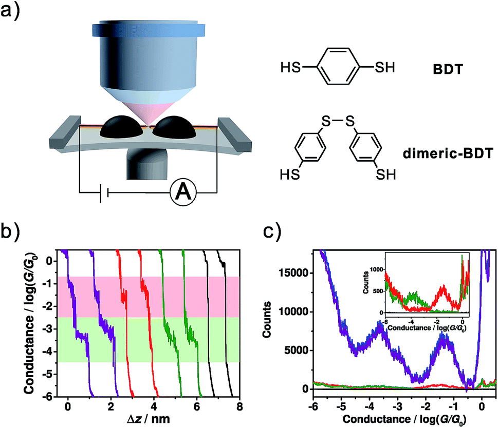 | ||
| Fig. 1 (a) Schematic of the MCBJ-SERS setup and the molecular structures of BDT and dimeric-BDT. (b) Four types of typical trace recorded using the MCBJ technique, consisting of ones with two conductance plateaus (purple), high conductance only (red), low conductance only (green), and no plateau (black). (c) Conductance histogram constructed from ∼5000 conductance-distance traces (blue, 4720 curves, offset by −10000 counts for comparison), as well as the conditional histograms that are constructed from those traces with two conductance plateaus (purple, 4508 curves, offset by −10000 counts for comparison), high conductance only (red, 134 curves), low conductance only (green, 67 curves) and no plateau (black, 11 curves), respectively. Inset: expansion of the red, green, and black conductance histograms with the scale shown from −100 to 1400 for better demonstration. | ||
The conductance histograms constructed from different types of trace are shown in Fig. 1c. The blue histogram constructed from all traces without data selection shows two pronounced peaks at 10−1.32±0.42G0 (high conductance) and 10−3.68±0.60G0 (low conductance), while the conductance histogram constructed from traces with only one conductance feature shows only one conductance peak (red and green histograms in the inset of Fig. 1c). The observed high conductance value is in agreement with some previous reports of BDT single-molecule junctions,14–16,39 while the low conductance value herein also agrees with some other reported conductance or secondary conductance features for BDT.1,16–18,40
To correlate the conductance and the distance between the two electrodes for high conductance and low conductance features, a 2D conductance-distance histogram was constructed from all of the traces. As shown in Fig. 2a, two prominent conductance clouds are found. The displacement distributions for the high conductance and low conductance features were analysed as follows. For the high conductance plateau, the length was defined as the distance between the points where the conductance fell in between 10−0.3G0 ∼ 10−2.5G0, while for the low conductance plateau it was defined as that between 10−0.3G0 ∼ 10−4.6G0. As shown in Fig. 2b, the most probable relative displacement for low conductance (0.72 ± 0.20 nm) is significantly longer than that of high conductance (0.39 ± 0.16 nm). The 0.33 nm difference in displacement suggests that low conductance and high conductance come from different molecular configurations. Considering that the snap-back distance is approximately 0.5 nm for a gold atomic contact,35 the length of the corresponding microscopic configuration for high conductance is 0.89 (0.39 plus 0.5) nm, which is close to the length of BDT (0.846 nm),18 thus suggesting that high conductance comes from a perpendicularly orientated configuration. More interestingly, taking into account the snap-back distance, for the low conductance the most probable displacement reaches 1.22 (0.72 plus 0.5) nm, which is around 0.4 nm longer than the length of BDT.16 This significant difference implies that the origin of the low conductance goes beyond a single-molecule BDT junction.
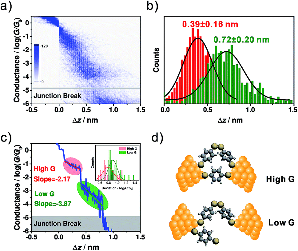 | ||
| Fig. 2 (a) The 2D conductance-distance histogram constructed from ∼5000 individual traces. (b) The relative displacement distributions for high conductance (red) and low conductance (green). (c) The master curve built from (a). Inset: the distributions of the conductance deviations from the master curve within the high conductance (red) and low conductance (green) regimes. Bin size: 0.02. (d) The hypothesized evolution of the microscopic configuration as the conductance evolves from high conductance to low conductance. | ||
A detailed distribution analysis of the different types of trace also indicated that both high conductance and low conductance plateaus appear simultaneously in 95.5% of the conductance-distance traces (see ESI Section 2 and Table S1† for more details). In contrast, the percentages of the traces with only high conductance or low conductance plateaus are 2.84% and 1.42%, respectively. There is a possible hypothesis that the low conductance comes from 4,4′-disulfanediyldibenzenethiol, i.e., dimeric-BDT, and the continuous appearance of two conductance features suggests the presence of parallel BDT and dimeric-BDT molecular junctions for the high conductance regime.
Fig. 1a shows the molecular structure of dimeric-BDT, where two BDT components are connected by a rotatable S–S single bond. Under ambient conditions, it has been demonstrated that BDT can convert to dimeric-BDT spontaneously as a result of oxidative dimerization.41 We estimated the effective conductive length of a dimeric-BDT molecule through density functional theory (DFT) calculation. As shown in Fig. S3,† the distance between the anchored gold atoms from the opposite electrodes was estimated to be 1.32 nm, which agrees well with our result that the length of the corresponding configuration for low conductance is 1.22 nm. Thus, Fig. 2d gives the framework of our hypothesis as follows: for the high conductance plateau, there is an Au/dimeric-BDT/Au single-molecule junction in parallel to the Au/BDT/Au single-molecule junction. As the electrode pair is stretched gradually, the Au/BDT/Au junction breaks firstly, and consequently the Au/dimeric-BDT/Au junction dominates charge transport and contributes to the low conductance plateau, which leads to the simultaneous appearance of high conductance and low conductance in individual traces.
To further investigate the configurational evolution behind the observed high conductance and low conductance, a master curve, which represents the most probable conductance-distance trace,35 was extracted and is shown in Fig. 2c. Here, the regimes for high conductance and low conductance are marked with red and green circles, respectively. The master curves and conductance variation analysis (Fig. 2c inset)35 indicated that the conductance fluctuation in the low conductance regime is much larger than that of the high conductance one. The larger conductance fluctuation implies that the structure of the molecular junction for low conductance has more freedom in its configurational variation, which may come from the flexibility of the S–S single bond formed in dimeric-BDT. We further analysed the displacement dependence of conductance in the master curve. For the high and low conductance plateaus of the master curve, the changing rates of the conductance along with the junction length were found to be −2.17log(G/G0)/nm for the high conductance regime (red line) and −3.87log(G/G0)/nm for the low conductance regime (green line), as shown in Fig. 2c. The deviation levels of the high and low conductance region were given by a Gaussian fit of the conductance deviation distributions (Fig. 2c inset). The deviation level of the high conductance regime agrees well with a previous report on rigid conjugated molecules with thiols as anchoring groups.35 Moreover, the larger deviation level of the low conductance regime indicates that the configuration for high conductance is more rigid than that of low conductance, which is consistent with the existence of BDT and dimeric-BDT.
The use of in situ SERS measurements offers a complementary approach besides single-molecule conductance characterization to verify our hypothesis of configurational evolution of the BDT junctions.
To detect the presence of an S–S bond for dimeric-BDT, we placed the MCBJ set-up under a Raman microscope with a 785 nm laser to activate the SPR inside the nanogap, as shown in Fig. 1a and S4 in the ESI.†
To avoid the appearance of a fluorescence background in the SERS spectra, a 785 nm laser was adopted. For the configuration of two facing nano-electrodes with nanometre-sized separation, it has been demonstrated that surface plasmon resonance (SPR) would be triggered inside the nano-gap when the electrode configuration was irradiated using a 785 nm laser.42–44 The SPR then greatly enhances the Raman signals, making it possible to get the signal of a single molecule. To perform in situ SERS characterization, the MCBJ setup was placed on a home-built platform under the Raman microscope. The laser spot was firstly positioned at different sites of the electrode pair to analyse the origin of the SERS signal, as shown in Fig. 3a. We measured the SERS signals at three different sites: the gap area (spot 1), the edge of the gap (spot 2), and the Au wire surface outside the gap (spot 3). For the signals collected from spot 2 and 3, the SERS intensity decreased significantly compared to that from spot 1. This observation agrees with previous reports,29,31,34 which indicates that for the molecules trapped between the two electrodes, the enhancement factor of the SERS signal increases significantly. Because the gold atoms constituting the Au/BDT/Au junction are the closest ones inside the gap area, the electromagnetic field achieved a maximum in the area of the Au/BDT/Au junction. As a result, BDT from the junction area has the largest enhancement factor during SERS characterization. Thus, among the molecules that are trapped within the nanogap, it can be further inferred that the Au/BDT/Au junction, rather than BDT molecules that are adsorbed on just one electrode, gives the major contribution to the obtained SERS signal.
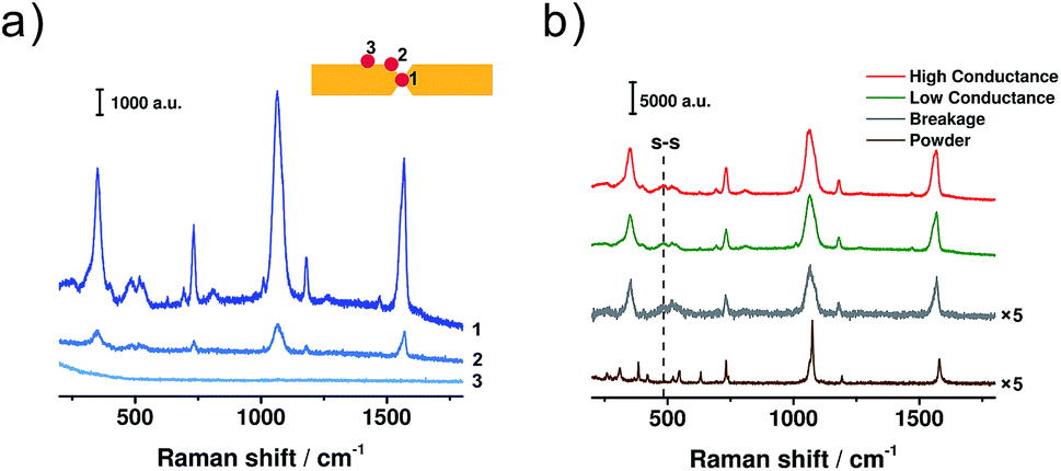 | ||
| Fig. 3 (a) SERS spectra of BDT collected from different sites of the electrode pair. Inset: the locations of the laser spot. (b) SERS spectra collected when the molecular junction was mechanically controlled at the regimes of high conductance (red), low conductance (green), and breakage (grey), respectively. An ordinary Raman spectrum of BDT powder (brown) is displayed for comparison. Laser excitation: 785 nm. | ||
Then we collected SERS spectra when the BDT single-molecule junction was controlled at the regimes of high conductance, low conductance and breakage, respectively, as shown in Fig. 3b. For these MCBJ-SERS spectra, the major bands can be assigned to the C–S stretching mode (354 cm−1, υ6a), ring breathing mode (1067 cm−1, υ1), C![[double bond, length as m-dash]](https://www.rsc.org/images/entities/char_e001.gif) C stretching mode (1569 cm−1, υ8a),18,45,46 as well as the ring mode of 7a (730 cm−1) and 9a (1180 cm−1).47 For comparison, the ordinary Raman spectrum of bare BDT powder was collected and is shown in Fig. 3b. In the ordinary Raman spectrum, the υ1 and υ8a modes appear at 1075 and 1579 cm−1 (see Fig. S5 in ESI† for details), while in the MCBJ-SERS spectra they are red-shifted to 1064 and 1569 cm−1, respectively. Through a combination of SERS study and quantum chemical calculation, we have demonstrated that the frequency shifts of these two modes can be used as a signature to verify the formation of a Au/BDT/Au junction.48,49 Thus the red shift observed here further confirms our inference that the Au/BDT/Au junction is responsible for the collected SERS signals. More significantly, a distinct peak appeared at 485 cm−1 during the SERS characterization, as highlighted by the dashed line in Fig. 3b. This peak has been recognized as the vibrational mode of the S–S bond,50,51 thus indicating the presence of dimeric-BDT during the conductance measurements. More interestingly, as shown in Fig. 3b, these two peaks appeared in both the regimes of high conductance and low conductance. Therefore, although at the regime of high conductance the conduction is dominated by BDT, the dimeric-BDT junction is also present at such a state, giving rise to the microscopic configuration as sketched in Fig. 2d.
C stretching mode (1569 cm−1, υ8a),18,45,46 as well as the ring mode of 7a (730 cm−1) and 9a (1180 cm−1).47 For comparison, the ordinary Raman spectrum of bare BDT powder was collected and is shown in Fig. 3b. In the ordinary Raman spectrum, the υ1 and υ8a modes appear at 1075 and 1579 cm−1 (see Fig. S5 in ESI† for details), while in the MCBJ-SERS spectra they are red-shifted to 1064 and 1569 cm−1, respectively. Through a combination of SERS study and quantum chemical calculation, we have demonstrated that the frequency shifts of these two modes can be used as a signature to verify the formation of a Au/BDT/Au junction.48,49 Thus the red shift observed here further confirms our inference that the Au/BDT/Au junction is responsible for the collected SERS signals. More significantly, a distinct peak appeared at 485 cm−1 during the SERS characterization, as highlighted by the dashed line in Fig. 3b. This peak has been recognized as the vibrational mode of the S–S bond,50,51 thus indicating the presence of dimeric-BDT during the conductance measurements. More interestingly, as shown in Fig. 3b, these two peaks appeared in both the regimes of high conductance and low conductance. Therefore, although at the regime of high conductance the conduction is dominated by BDT, the dimeric-BDT junction is also present at such a state, giving rise to the microscopic configuration as sketched in Fig. 2d.
To further test our hypothesis that the low conductance comes from the dimeric-BDT junction, two control experiments were performed. The first one was tuning the formation probability of dimeric-BDT. Herein, 0.1 mM tris(2-carboxyethyl)phosphine hydrochloride (TCEP), a reagent widely used to disrupt disulfide bonds,52 was prepared in a mixed solvent of EtOH and TMB (v/v = 1:9), and then added into the BDT solution that was to be assayed through single-molecule conductance measurements. It was found that the intensity of the high conductance peak remained unchanged after adding TCEP (Fig. 4a). In contrast, the low conductance peak in the 1D conductance histogram (Fig. 4a), as well as the intensity cloud of low conductance in the 2D conductance histogram (Fig. 4b), became inconspicuous. This observation indicates that TCEP prevents the occurrence of the configuration that accounts for low conductance, which agrees well with the existence of dimeric-BDT. Secondly, the possibility that the low conductance feature results from the formation of a π–π stacking configuration needs to be eliminated.53,54 We employed pentane-1,5-dithiol (PDT) as the probe molecule since it has no π conjugated component. Thus, a π–π stacking configuration could not be formed during the measurement, while the disulfide configuration was still formed and caused a lower conductance. It was found that the 1D conductance histogram for PDT exhibited two conductance peaks, similar to that of BDT. Moreover, the lower one can be restrained using TCEP as well (see Section 8 in ESI† for details). Therefore, for both BDT and PDT, it is the disulfide configuration, rather than the π–π stacking configuration,53,54 that should be ascribed to the low conductance.
 | ||
| Fig. 4 (a) Conductance histograms of BDT before (blue) and after (red) the addition of TCEP. (b) 2D conductance-distance histogram of BDT after the addition of TCEP. | ||
Conclusions
In summary, we investigated the charge transport through a BDT single-molecule junction with a combined MCBJ and in situ SERS approach. Two distinct conductance features were found to appear simultaneously in the single-molecule conductance measurements. It was also found that there is a ∼0.33 nm difference in the displacement between the lengths of the high conductance and low conductance plateaus. The length for the low conductance feature is significantly longer than the molecular length of BDT, but is in agreement with that of the dimeric-BDT junction. To further confirm the presence of dimeric-BDT, the signal of an S–S single bond was observed using in situ SERS for both the high and low conductance states. These results revealed that it is dimeric-BDT, rather than BDT itself, that contributes to the low conductance feature. Control experiments demonstrate that disulfide-mediated dimerization could be tuned via the chemical inhibitor. Our findings suggest that the detection of a chemical reaction will also contribute to the discrepancy in single-molecule conductance measurements, which provide a novel avenue for the design and fabrication of molecular devices at the single-molecule scale.Conflicts of interest
There are no conflicts to declare.Acknowledgements
This work was supported by the National Key R&D Program of China (2017YFA0204902), the National Natural Science Foundation of China (21673195, 21503179, 61573295, 21703188, and 21722305), the Fundamental Research Funds for the Central Universities (Xiamen University: 20720170035), the Natural Science Foundation of Fujian Province (2016J05162), the China Postdoctoral Science Foundation (2017M622060), the National Basic Research Program of China (2015CB932301), and the Young Thousand Talent Project of China.Notes and references
- M. A. Reed, C. Zhou, C. J. Muller, T. P. Burgin and J. M. Tour, Science, 1997, 278, 252–254 CrossRef.
- B. Xu and N. J. Tao, Science, 2003, 301, 1221–1223 CrossRef PubMed.
- H. Song, Y. Kim, Y. H. Jang, H. Jeong, M. A. Reed and T. Lee, Nature, 2009, 462, 1039–1043 CrossRef PubMed.
- A. C. Aragonès, N. L. Haworth, N. Darwish, S. Ciampi, N. J. Bloomfield, G. G. Wallace, I. Diez-Perez and M. L. Coote, Nature, 2016, 531, 88 CrossRef PubMed.
- C. Jia and X. Guo, Chem. Soc. Rev., 2013, 42, 5642–5660 RSC.
- K. Wang, J. M. Hamill, B. Wang, C. Guo, S. Jiang, Z. Huang and B. Xu, Chem. Sci., 2014, 5, 3425–3431 RSC.
- L. Gao, L.-L. Li, X. Wang, P. Wu, Y. Cao, B. Liang, X. Li, Y. Lin, Y. Lu and X. Guo, Chem. Sci., 2015, 6, 2469–2473 RSC.
- C. Huang, A. V. Rudnev, W. Hong and T. Wandlowski, Chem. Soc. Rev., 2015, 44, 889–901 RSC.
- R. J. Nichols and S. J. Higgins, Acc. Chem. Res., 2016, 49, 2640–2648 CrossRef PubMed.
- L. Gerhard, K. Edelmann, J. Homberg, M. Valášek, S. G. Bahoosh, M. Lukas, F. Pauly, M. Mayor and W. Wulfhekel, Nat. Commun., 2017, 8, 14672 CrossRef PubMed.
- H. Häkkinen, Nat. Chem., 2012, 4, 443 CrossRef PubMed.
- M. Strange, O. Lopez-Acevedo and H. Häkkinen, J. Phys. Chem. Lett., 2010, 1, 1528–1532 CrossRef.
- M. Taniguchi, M. Tsutsui, K. Yokota and T. Kawai, Chem. Sci., 2010, 1, 247–253 RSC.
- X. Y. Xiao, B. Q. Xu and N. J. Tao, Nano Lett., 2004, 4, 267–271 CrossRef.
- M. Tsutsui, M. Taniguchi and T. Kawai, Nano Lett., 2009, 9, 2433–2439 CrossRef PubMed.
- Y. Kim, T. Pietsch, A. Erbe, W. Belzig and E. Scheer, Nano Lett., 2011, 11, 3734–3738 CrossRef PubMed.
- Y. Yang, J. Liu, S. Feng, H. Wen, J. Tian, J. Zheng, B. Schöllhorn, C. Amatore, Z. Chen and Z. Tian, Nano Res., 2016, 9, 560–570 CrossRef.
- S. Kaneko, D. Murai, S. Marqués-González, H. Nakamura, Y. Komoto, S. Fujii, T. Nishino, K. Ikeda, K. Tsukagoshi and M. Kiguchi, J. Am. Chem. Soc., 2016, 138, 1294–1300 CrossRef PubMed.
- C. Bruot, J. Hihath and N. Tao, Nat. Nanotechnol., 2012, 7, 35–40 CrossRef PubMed.
- S. Nie and S. R. Emory, Science, 1997, 275, 1102–1106 CrossRef PubMed.
- F. Benz, M. K. Schmidt, A. Dreismann, R. Chikkaraddy, Y. Zhang, A. Demetriadou, C. Carnegie, H. Ohadi, B. de Nijs, R. Esteban, J. Aizpurua and J. J. Baumberg, Science, 2016, 354, 726–729 CrossRef PubMed.
- Y.-L. Ying, Z. Ding, D. Zhan and Y.-T. Long, Chem. Sci., 2017, 8, 3338–3348 RSC.
- A. I. Yanson, G. R. Bollinger, H. E. van den Brom, N. Agraït and J. M. van Ruitenbeek, Nature, 1998, 395, 783–785 CrossRef.
- Y. S. Park, A. C. Whalley, M. Kamenetska, M. L. Steigerwald, M. S. Hybertsen, C. Nuckolls and L. Venkataraman, J. Am. Chem. Soc., 2007, 129, 15768–15769 CrossRef PubMed.
- S.-P. Liu, S. H. Weisbrod, Z. Tang, A. Marx, E. Scheer and A. Erbe, Angew. Chem., Int. Ed., 2010, 49, 3313–3316 CrossRef PubMed.
- Y. Kim, H. Song, F. Strigl, H.-F. Pernau, T. Lee and E. Scheer, Phys. Rev. Lett., 2011, 106, 196804 CrossRef PubMed.
- P. Makk, D. Tomaszewski, J. Martinek, Z. Balogh, S. Csonka, M. Wawrzyniak, M. Frei, L. Venkataraman and A. Halbritter, ACS Nano, 2012, 6, 3411–3423 CrossRef PubMed.
- I. W. P. Chen, W. H. Tseng, M. W. Gu, L. C. Su, C. H. Hsu, W. H. Chang and C. h. Chen, Angew. Chem., Int. Ed., 2013, 52, 2449–2453 CrossRef PubMed.
- J.-H. Tian, B. Liu, X. Li, Z.-L. Yang, B. Ren, S.-T. Wu, N. Tao and Z.-Q. Tian, J. Am. Chem. Soc., 2006, 128, 14748–14749 CrossRef PubMed.
- T. Konishi, M. Kiguchi, M. Takase, F. Nagasawa, H. Nabika, K. Ikeda, K. Uosaki, K. Ueno, H. Misawa and K. Murakoshi, J. Am. Chem. Soc., 2013, 135, 1009–1014 CrossRef PubMed.
- D. R. Ward, N. J. Halas, J. W. Ciszek, J. M. Tour, Y. Wu, P. Nordlander and D. Natelson, Nano Lett., 2008, 8, 919–924 CrossRef PubMed.
- H. P. Yoon, M. M. Maitani, O. M. Cabarcos, L. Cai, T. S. Mayer and D. L. Allara, Nano Lett., 2010, 10, 2897–2902 CrossRef PubMed.
- Z. Liu, S.-Y. Ding, Z.-B. Chen, X. Wang, J.-H. Tian, J. R. Anema, X.-S. Zhou, D.-Y. Wu, B.-W. Mao, X. Xu, B. Ren and Z.-Q. Tian, Nat. Commun., 2011, 2, 305 CrossRef PubMed.
- T. Shamai and Y. Selzer, Chem. Soc. Rev., 2011, 40, 2293–2305 RSC.
- W. Hong, D. Z. Manrique, P. Moreno-García, M. Gulcur, A. Mishchenko, C. J. Lambert, M. R. Bryce and T. Wandlowski, J. Am. Chem. Soc., 2012, 134, 2292–2304 CrossRef PubMed.
- D. Z. Manrique, C. Huang, M. Baghernejad, X. Zhao, O. A. Al-Owaedi, H. Sadeghi, V. Kaliginedi, W. Hong, M. Gulcur, T. Wandlowski, M. R. Bryce and C. J. Lambert, Nat. Commun., 2015, 6, 6389 CrossRef PubMed.
- G. D. Harzmann, R. Frisenda, H. S. J. van der Zant and M. Mayor, Angew. Chem., Int. Ed., 2015, 54, 13425–13430 CrossRef PubMed.
- G. Yang, S. Sangtarash, Z. Liu, X. Li, H. Sadeghi, Z. Tan, R. Li, J. Zheng, X. Dong, J. Liu, Y. Yang, J. Shi, Z. Xiao, G. Zhang, C. Lambert, W. Hong and D. Zhang, Chem. Sci., 2017, 8, 7505–7509 RSC.
- Y. Yang, Z. Chen, J. Liu, M. Lu, D. Yang, F. Yang and Z. Tian, Nano Res., 2011, 4, 1199–1207 CrossRef.
- J. Ulrich, D. Esrail, W. Pontius, L. Venkataraman, D. Millar and L. H. Doerrer, J. Phys. Chem. B, 2006, 110, 2462–2466 CrossRef PubMed.
- L. Wang, S.-Y. Li, J.-H. Yuan, J.-Y. Gu, D. Wang and L.-J. Wan, Chem.–Asian J., 2014, 9, 2077–2082 CrossRef PubMed.
- A. Garcia-Martin, D. R. Ward, D. Natelson and J. C. Cuevas, Phys. Rev. B: Condens. Matter Mater. Phys., 2011, 83, 193404 CrossRef.
- K. J. Savage, M. M. Hawkeye, R. Esteban, A. G. Borisov, J. Aizpurua and J. J. Baumberg, Nature, 2012, 491, 574–577 CrossRef PubMed.
- D. R. Ward, D. A. Corley, J. M. Tour and D. Natelson, Nat. Nanotechnol., 2011, 6, 33–38 CrossRef PubMed.
- S. F. Shi, X. Xu, D. C. Ralph and P. L. McEuen, Nano Lett., 2011, 11, 1814–1818 CrossRef PubMed.
- R. Matsuhita, M. Horikawa, Y. Naitoh, H. Nakamura and M. Kiguchi, J. Phys. Chem. C, 2013, 117, 1791–1795 Search PubMed.
- S. H. Cho, H. S. Han, D.-J. Jang, K. Kim and M. S. Kim, J. Phys. Chem., 1995, 99, 10594–10599 CrossRef.
- Y.-F. Huang, N.-N. Yin, X. Wang, D.-Y. Wu, B. Ren and Z.-Q. Tian, Chem.–Eur. J., 2010, 16, 1449–1453 CrossRef PubMed.
- S. Suzuki, S. Kaneko, S. Fujii, S. Marqués-González, T. Nishino and M. Kiguchi, J. Phys. Chem. C, 2016, 120, 1038–1042 Search PubMed.
- S. W. Joo, S. W. Han and K. Kim, J. Colloid Interface Sci., 2001, 240, 391–399 CrossRef PubMed.
- M. Sun, L. Xia and M. Chen, Spectrochim. Acta, Part A, 2009, 74, 509–514 CrossRef PubMed.
- J. A. Burns, J. C. Butler, J. Moran and G. M. Whitesides, J. Org. Chem., 1991, 56, 2648–2650 CrossRef.
- S. Wu, M. T. González, R. Huber, S. Grunder, M. Mayor, C. Schönenberger and M. Calame, Nat. Nanotechnol., 2008, 3, 569 CrossRef PubMed.
- J.-T. Zheng, R.-W. Yan, J.-H. Tian, J.-Y. Liu, L.-Q. Pei, D.-Y. Wu, K. Dai, Y. Yang, S. Jin and W. Hong, Electrochim. Acta, 2016, 200, 268–275 CrossRef.
Footnotes |
| † Electronic supplementary information (ESI) available. See DOI: 10.1039/c8sc00727f |
| ‡ These authors contributed equally. |
| This journal is © The Royal Society of Chemistry 2018 |