
 Open Access Article
 This Open Access Article is licensed under a Creative Commons Attribution-Non Commercial 3.0 Unported Licence
A first-principles prediction on the “healing effect” of graphene preventing carrier trapping near the surface of metal halide perovskites†
W.-W.
Wang
ab,
J.-S.
Dang
ab,
R.
Jono
 a,
H.
Segawa
*a and
M.
Sugimoto
*ab
a,
H.
Segawa
*a and
M.
Sugimoto
*ab
aResearch Center for Advanced Science and Technology, The University of Tokyo, 4-6-1 Komaba, Meguro-ku, Tokyo 153-8904, Japan. E-mail: csegawa@mail.ecc.u-tokyo.ac.jp
bFaculty of Advanced Science and Technology, Kumamoto University, 2-39-1 Kurokami, Chuo-ku, Kumamoto 860-8555, Japan. E-mail: sugimoto@kumamoto-u.ac.jp
First published on 22nd February 2018
Abstract
We herein report that surface modification of metal halide perovskites using graphene would be beneficial to improving the energy conversion efficiencies of perovskite solar cells. The present first-principles calculations on MAPbI3 with a single vacancy created by removing either I, Pb or MA show that the I and Pb vacancies near the surface result in the formation of Pb–Pb and I–I dimers, respectively. They are predicted to yield mid-gap levels, and would degrade the energy conversion efficiency of perovskite solar cells through carrier trapping. The present calculations suggest that when the surface of MAPbI3 is covered with a graphene sheet, the formation of the carrier trapping dimers would be suppressed. The origin of the “healing effect” of graphene on the lattice defect is ascribed to electronic interactions on the surface, which prevent charge localization at the lattice defects beneath the surface.
1 Introduction
Metal halide perovskites (e.g. methylammonium lead iodide (MAPbI3)) have been proved to be promising materials for photovoltaic applications because of their feasible and tunable band gaps,1 high and balanced charge-carrier mobilities,2 and long electron–hole diffusion lengths.3 In particular, the power conversion efficiency (PCE) of perovskite solar cells (PSCs) has dramatically increased from 3.8% in 2009 to a recently certified 22.1%.4,5 Despite the impressive development, current efficiencies of PSCs are still far from the theoretical maximum of 30–33%.6,7 One important issue is the effect of perovskite defects which is strongly related to the electrical instability and formation of charge trapping states.7 In particular, the defect-mediated interfacial carrier (hole and electron) recombination process is considered as an important loss mechanism of perovskite solar cells.8 Previous studies have proposed that defects or impurities of perovskite thin films prefer to be concentrated at the grain boundaries and interface between the perovskite and the neighbouring charge transporting layers,9–13 which assist non-radiative carrier recombination and significantly affect the short-circuit current and open-circuit voltage of devices.To avoid the defect-induced interfacial traps, careful control of the perovskite crystallinity and interface optimization via incorporation of additional materials are two feasible strategies in practice.14–22 Among the limited studies that made efforts to understand the role of surface defects and detrapping mechanisms,7,16,17,23,24 the incorporation of PCBM ([6,6]-phenyl-C61-butyric acid methyl ester) was reported as a unique way to reduce trap states caused by Pb–I antisite defects.16,17 Experimental evidence indicated that PCBM distributes around the perovskite surface and passivates the antisite defects via electron transfer with anionic iodines.17 As a result the recombination and current–voltage (J–V) hysteresis are suppressed and the device performance is correspondingly improved.
Besides fullerene and its derivatives, graphene is another promising sp2 nano-carbon material which has been widely used in PSCs as an interlayer to achieve improved contact between the perovskite and the neighbouring charge transporting layers, better charge transport characteristics, and enhanced device stabilities.25–34 However, to date, there have been hardly any investigations on the role of graphene in interface modification and the relationship between graphene and surface defects of perovskites. Of particular interest is the understanding of defective vacancies at the surface in the presence of graphene. Compared to other types of point defects, single vacancies of MAPbI3 perovskites, including iodine vacancies, lead vacancies, and MA vacancies, are considered as a major type of structural defects because of their relatively low formation energies.7,8,35 So far most studies on perovskite vacancies have mainly focused on intrinsic defects which are believed to not form deep-level defects for carrier trapping.8,35–44 In contrast, systematic investigations on defective perovskites with surface vacancies are still limited.45,46 Therefore it is of great interest to explore the nature of vacancy defects around the perovskite surface as well as the role of graphene on the surface.
In the present work, first-principles calculations were carried out to study the properties of defective perovskite MAPbI3 with single vacancies. The results showed that the I or Pb vacancies around the surface region are prone to generate deep-level defects by producing Pb–Pb or I–I dimers, respectively. What is more important is that the incorporation of a graphene layer on the top of the perovskite gives rise to the modification of defective sites and the trap states are effectively eliminated, which can be attributed to the interfacial charge transfer between graphene and surface Pb or I atoms. In addition, this healing effect by the incorporation of an interlayer was extended to the use of small organic molecules. The results showed that surface passivation by employing electron-deficient hydrocarbons (e.g. ethylene and benzene) or molecules with a lone pair (e.g. pyridine) can also eliminate the trap states induced by surface vacancies.
2. Computational methods
First-principles calculations were performed using density functional theory in the CASTEP code.47,48 The Perdew–Burke–Ernzerhof (PBE) generalized gradient approximation was used to describe the exchange–correlation interactions.49 Tkatchenko–Scheffler (TS) custom DFT-D parameters were adopted to describe the empirical dispersion correction.50 The ionic cores and core–valence interactions were described using the ultrasoft pseudopotentials, and the kinetic energy cutoff was set to 500 eV.51The tetragonal MAPbI3 (β-phase) was used as the perovskite material. In this work we investigated all three types of single vacancies of MAPbI3, i.e. iodine vacancy (VI), lead vacancy (VPb), and MA vacancy (VMA). Both the supercell and slab models were employed to explore the influence of vacancies in different positions (bulk or surface region of crystals). Note that the defective structures with single vacancies are studied in neutral states. The bulk tetragonal-MAPbI3 was optimized using a  supercell containing 32 formula units (17.600 × 17.600 × 25.370 Å3), as shown in Fig. 1. For slab calculations, discussions in the present work were mainly focused on a 2 × 2 × 3.5 tetragonal-MAPbI3 model (Slab1, see Fig. 1) with a (110)-surface which was determined to be one of the most predominant MAPbI3 facets in experiments,52 with a calculated band gap of 1.352 eV (Table S1 of the ESI†). Moreover, the constructed slab model is terminated by a PbI2 layer rather than a MAI layer because our calculations based on two smaller 2 × 2 × 2.5 MAPbI3 slabs (labelled Slab2 and Slab3 in Fig. S1 of the ESI†) show that the binding energy (Eb) of the PbI2–graphene interface is 0.41 eV larger than that of the MAI–graphene interface (see Table S2 and Fig. S2 of the ESI†). In addition, to check the influence of slab size on the results, calculations were repeated by using a larger 4 × 2 × 2.5 structure (Slab4 in Fig. S1 of the ESI†). The results (Fig. S3 of the ESI†) showed that similar properties can be obtained by using different slab models, indicating that the slabs we used are large enough to get reliable outcomes. Note that the Brillouin zone was described using 1 × 1 × 1 for the bulk model and 2 × 2 × 1 (Slab1)/4 × 4 × 1 (Slab2 and Slab3)/1 × 2 × 1 (Slab4) grids for different slab structures. As for the graphene incorporated hybrid structures, experimental lattice constants of MAPbI3 were adopted (with an average Pb–Pb distance of 6.263 Å) during geometry relaxations,53 and the lattice mismatch between MAPbI3 and graphene was 1% only. It is worth noting that a vacuum region of more than 25 Å was used for each slab model, in order to avoid interactions between periodic images. The atomic positions were fully relaxed for the optimization of each slab model in the present work.
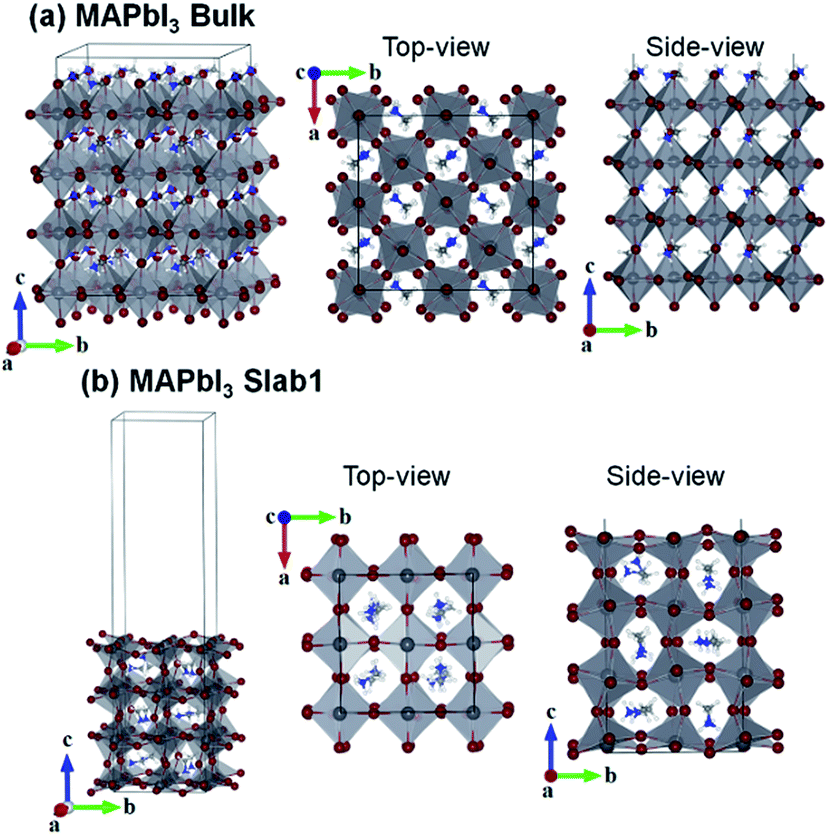 | ||
| Fig. 1 (a) Bulk and (b) slab MAPbI3 models adopted in the present study. | ||
3 Results and discussion
3.1. MAPbI3 with an I vacancy
First, we focused on the defective perovskites with a single iodine vacancy (VI). For a bulk tetragonal-MAPbI3 model with this point defect, geometry optimization showed that structural relaxation around the VI is small and the bulk structure is maintained. This is reflected in the Pb–Pb distance near the VI. It was calculated to be 6.278 Å (Fig. S4 of the ESI†), which is comparable to that in the bulk (6.263 Å). The calculated density of states (DOS) (see Fig. S5 of the ESI†) reveals that the VI in the bulk gives rise to a shallow-level defect below the conduction band edge. Since the VI is formed by removing a neutral I atom in the present modelling, this shallow level is occupied by an electron. Thus, this defective system exhibits an n-type character. These features of the bulk defect are essentially similar to those reported by Zhang et al.8In order to investigate the surface of MAPbI3 with a VI, we employed four types of 3.5-layered tetragonal-MAPbI3 slab models with a single VI labelled Slab1_VI-1, -2, -3, and -4, given in Fig. 2. In these models, the position of the VI is different. The VI resides around the surface region in Slab1_VI-1 (on the PbI2 layer) and Slab1_VI-2 (on the MAI layer), whereas it locates at intrinsic positions in cases of Slab1_VI-3 (on the PbI2 layer) and Slab1_VI-4 (on the MAI layer). As mentioned above, compared to the well-studied intrinsic vacancies in bulk, the characteristics of surface and interfacial vacancies of perovskites are still rarely known. For comparison, the perfect (defect-free) slab model was also optimized by using DFT calculations.
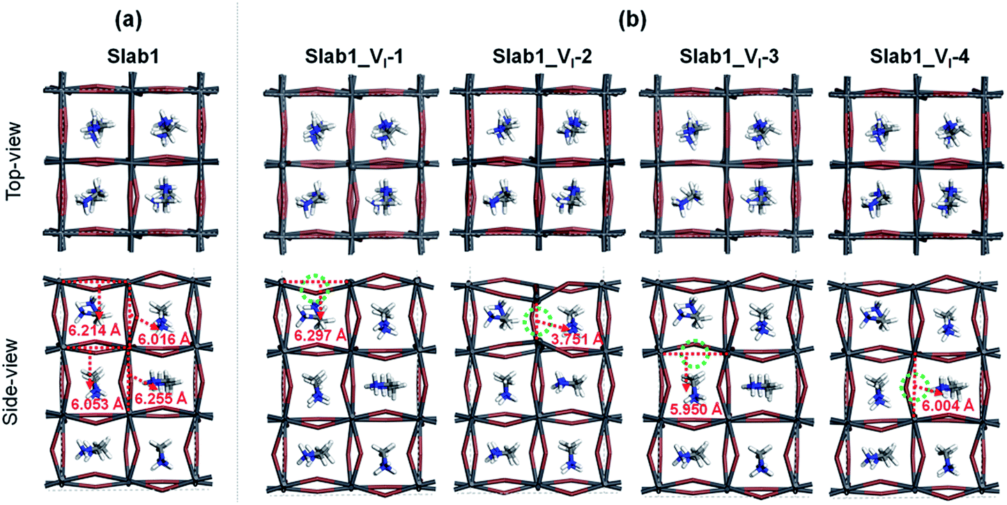 | ||
| Fig. 2 (a) Defect-free and (b) VI-containing defective MAPbI3 slabs. The dashed circles indicate the position of the VI. Each number in (b) indicates the Pb–Pb distance around the VI. | ||
Among the optimized structural parameters, we find a notable change in Slab1_VI-2 (Fig. 2(b)): the Pb–Pb distance around the VI, which is perpendicular to the (110)-surface (a,b-plane), is greatly shortened to 3.751 Å. This is in sharp contrast to the corresponding Pb–Pb distance (6.016 Å) in the defect-free slab model. In Slab1_VI-1, -3, and -4, the Pb–Pb distances near the VI are 6.297, 5.950, and 6.004 Å, respectively. These values are close to those in the defect-free slab and aforementioned bulk models with a VI.
The features of the geometry changes are well reflected in the density of states (DOS) of the Slab1_VI models where the Fermi level (the highest occupied level) is set to 0 eV. The Fermi level in the defect-free slab model is located at the top of the valence band as shown in Fig. 3. The band gap of this model is 1.352 eV, which is comparable to the experimental value of 1.52 eV.54Fig. 4(a) shows the DOS of the defective slab model of Slab1_VI before geometry optimization. These data indicate that when a neutral I atom is removed, the Fermi level is located at the conduction band edge. The DOSs of the conduction band of the defective systems are essentially similar. This is also true except that the valence band onset of Slab_VI-1 is slightly shifted to low energy.
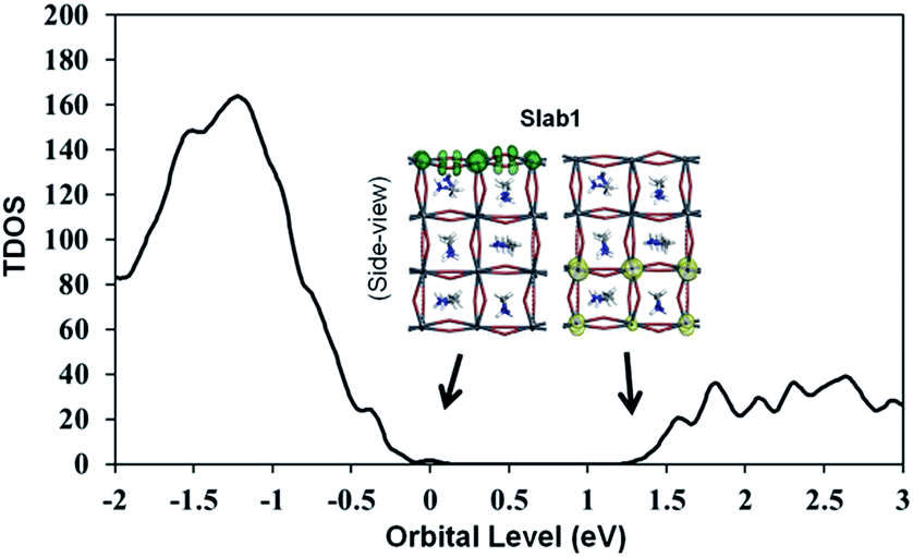 | ||
| Fig. 3 Calculated total density of states (TDOS) of the defect-free Slab1. The insets indicate the orbital shape of band edges. | ||
 | ||
| Fig. 4 Calculated total density of states (TDOS) of the VI-containing MAPbI3 slab models (a) before geometry optimization, (b) after geometry optimization, and (c) after geometry optimization where the valence band tops of all the defective slab models were adjusted to the same level. The inset in (c) indicates the orbital shape. | ||
After geometry optimization, the DOS of Slab_VI-2 becomes different from those of the other three systems as shown in Fig. 4(b). In the former, the conduction band bottom splits into two moieties, and the low-energy band becomes distinct. In order to highlight this feature, the valence band tops of the four models are shifted to take the same energy level in Fig. 4(c). In this figure, it is evident that the Slab_VI-2 model has a discrete energy level within the band gap. As shown in Fig. 5, this level is assigned to the orbital localized at the VI in Slab1_VI-2. It should be noted that the orbital shape clearly shows the bonding character of the Pb2 dimer at the position of the VI. Therefore, we can conclude that the discrete level is due to electron localization at the VI on which bonding interaction occurs between the two adjacent Pb atoms. In the other Slab1_VI models, the DOS data do not imply charge localization. This is consistent with the nearly unchanged Pb–Pb distance discussed above.
 | ||
| Fig. 5 The orbital shape of the conduction band edges (isovalue: 0.015 a.u.) of (a) the VI-containing MAPbI3 slab model before geometry optimization and (b) the VI-containing MAPbI3 slab model after geometry optimization. | ||
Since the electron localization results in the mid-gap level and the shortening of the adjacent Pb–Pb distance, it seems interesting to investigate the influence of excess charge doped in the present system. Zhang et al. reported that two Pb atoms of MAPbI3 around an intrinsic VI can form a dimer when an extra electron is captured into the defective system.8 Since this suggests that the charge state would play an essential role in structural distortion near the VI site, the Hirshfeld charge distribution of perfect and defective perovskite models were examined. In comparison with the defect-free MAPbI3 slab, we found that the total electron density of the two Pb atoms around the VI increases by 0.15 e (e: electrons) in Slab1_VI-2 (0.09 and 0.06 e for the Pb in the first and second layers, respectively). For other neutral VI-containing slabs, the increase of the electron population on the two dangling Pb atoms is only 0.04 e, 0.08 e, and 0.06 e in Slab1_VI-1, Slab1_VI-3, and Slab1_VI-4, respectively (Fig. S6 of the ESI†). It is evident that the dimerization can be related to electron localization. A similar feature was pointed out by Zhang.8
To further uncover the influence of charge localization in the defective system, geometry optimizations were performed on the positively and negatively charged VI-containing MAPbI3. As shown in Fig. S7–S10 of the ESI,† when one electron is doped, dimerization of Pb around the defective site is observed not only in Slab1_VI-2− but also in Slab1_VI-3− and Slab1_VI-4−. The calculated Pb–Pb distances are 3.575 Å (Fig. S8†), 3.523 Å (Fig. S9†), and 3.527 Å (Fig. S10†), respectively. These data indicate that the VI functions as an electron trap at the interface in perovskite solar cells. The present data imply that the VI in the inner region (away from the surface) would capture an electron when the electron concentration is high in a photovoltaic device.
In contrast, when the defective MAPbI3 models are positively (+1) charged, the Pb–Pb dimer does not form in any case (see Fig. S7–S10 of the ESI†). This suggests that the formation of the Pb–Pb dimer around the VI is strongly related not to hole localization but to electron localization in defective metal halide perovskites. Therefore, we can conclude that the VI would cause lowering of the energy conversion efficiency in perovskite solar cells by electron trapping. This lattice defect would be problematic, in particular, at the interface with the electron transport layer.
Next, we focused on graphene (G) + MAPbI3 hybrid systems by using the above-mentioned slab models in order to investigate the impact of coating graphene on geometrical and electronic structure modifications of defective perovskites. Here a single-layered graphene cell containing 60 carbon atoms was used to coat the perovskite surface (see the computational details). The optimized perfect/defective G + MAPbI3 hybrid structures are depicted in Fig. 6.
 | ||
| Fig. 6 (a) Defect-free and (b) VI-containing defective graphene + MAPbI3 hybrids. | ||
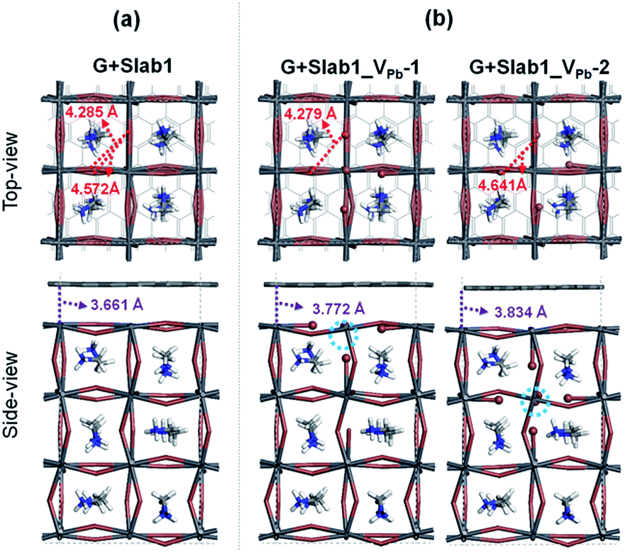
Two remarkable geometrical characteristics can be detected. In comparison with the bare state (Fig. 2), the PbI2 surface of MAPbI3 is flattened in the presence of the graphene coat, which can be elucidated by interfacial interactions consisting of both Pb–π and I–π effects. A similar surface modification has been reported in the case of hybridization between graphene and a defect-free γ-MAPbI3.55 The other feature is that the Pb2 dimer of the defective Slab1_VI-2 model is broken after graphene binding, with an extended Pb–Pb distance of 6.806 Å. It should be noted that the cleavage of Pb–Pb was also observed in the case of negatively charged Slab1_VI-2−. However, for the negatively charged Slab1_VI-4− in which the dimer resides in the bulk position, the Pb–Pb segment still exists with the incorporation of graphene (Fig. S11 and S12 of the ESI†). These results suggest that the stretching of Pb–Pb can be attributed to the surface Pb–π interactions.
The binding energies of complexes (Eb = E(Slab1) + E(G) − E(hybrid)) are listed in Table S3 of the ESI.† The results reveal that the hybridization is an exothermic process and the calculated Eb values among different perovskite slabs are very similar, implying that the introduction of a single I vacancy does not modify the interface stability remarkably. In addition, we investigated the distortion energy (Ed) of the perovskite and graphene after hybridization. The results collected in Table S3 of the ESI† showed that the structural distortion of graphene is very small (<0.03 eV) whereas the modification on the perovskite is significant (>0.1 eV). The deformation of MAPbI3 is mainly attributed to the flattened surface as mentioned before, and in particular, the Ed of Slab1_VI-2 (0.347 eV) is much larger than that of other models because of the energy requirement for Pb–Pb dimer cleavage, which can be further confirmed by the calculated pair formation energy (Ep) of the Pb–Pb dimer (0.371 eV) shown in Table S4 of the ESI.†
In order to explain the modification of perovskites after binding with graphene, the electron distributions of the hybrid systems were further investigated. The calculated Hirshfeld charge shows that the perovskite acts as an electron donor as shown in Table 1. The total number of electrons transferred from Slab1, Slab1_VI-1, Slab1_VI-2, Slab1_VI-3, and Slab1_VI-4 is 0.20, 0.37, 0.34, 0.20, and 0.23 e, respectively. This indicates two characteristics of the graphene layer. One is that graphene functions as a hole-injecting material. This is due to the fact that the Fermi level of graphene is located at the bottom of the conduction band of the defective MAPbI3 layer. Another characteristic is that more electrons are injected into graphene when the VI exists on the surface. This is because the surface state (or the surface/subsurface Pb atoms) would be more influenced by the VI in comparison with the bulk state (or the Pb atoms in the bulk).
| Structure | Graphene | Slab1_VI | |
|---|---|---|---|
| Dangling Pb atoms | The rest in total | ||
| a Averaged value (0.285 e per one Pb atom). | |||
| G + Slab1 | −0.20 | (+0.57)a | (−0.57) |
| G + Slab1_VI-1 | −0.37 | +0.67(+0.61) | −0.30(−0.61) |
| G + Slab1_VI-2 | −0.34 | +0.66(+0.45) | −0.32(−0.45) |
| G + Slab1_VI-3 | −0.20 | +0.43(+0.43) | −0.23(−0.43) |
| G + Slab1_VI-4 | −0.23 | +0.45(+0.44) | −0.22(−0.44) |
It is interesting to see the change of electron distribution of the two dangling Pb atoms around the VI before and after the graphene coating (Fig. S6 and S13 of the ESI†). In Slab1_VI-2 having the Pb–Pb dimer, 0.34 e are removed from MAPbI3: 0.21 e are taken from the dimer, while 0.13 e are taken from the rest of the crystal. On the other hand, in Slab1_VI-1, 0.37 e are removed from the perovskite layer. Only 0.06 e are taken from the dangling Pb atoms, while 0.31 e are taken from the rest of the crystal. This indicates that the hole injected into the two slab models distributes over the lattice and the electron localization on the dangling Pb seen in Slab1_VI-2 is relaxed.
The electron density difference (EDD) of the G + MAPbI3 hybrids (defined as EDD = ρ(hybrid) − ρ(Slab1) − ρ(G)) also suggests that the interactions between graphene and the unsaturated Pb atoms on the surface of either Slab1_VI-1 or Slab1_VI-2 are much stronger than those observed in the other systems (Fig. 7). In Slab1_VI-2, we see that the Pb atom just above the VI is largely oxidized by graphene. This implies that the local cation–π interaction on the dangling Pb atom on the top layer would occur. This enhanced local interaction would be the reason for the healing effect (removal of the dimer) around the VI.
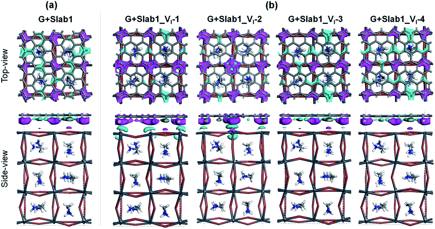 | ||
| Fig. 7 Electron density difference of the (a) defect-free and (b) VI-containing graphene + MAPbI3 hybrids (isovalue: 0.003 a.u.). Purple and cyan represent accumulation and depletion of electrons, respectively. | ||
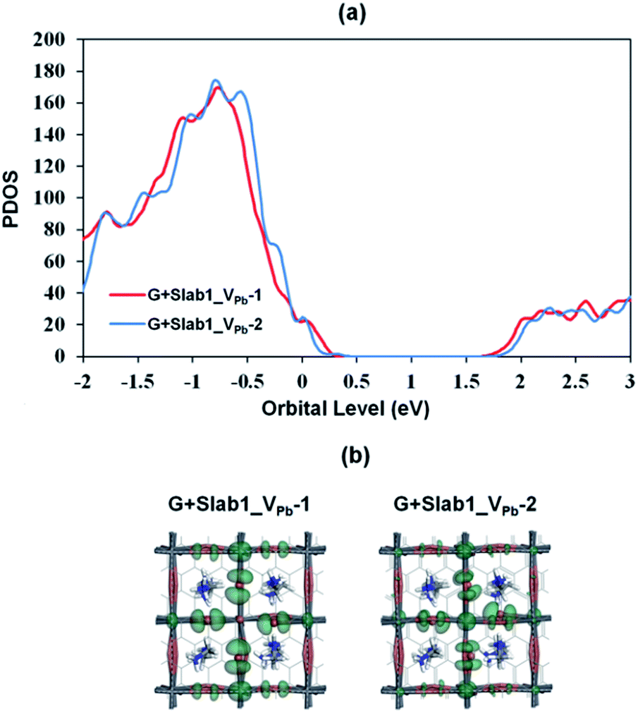
Since the Pb–Pb dimer, which was proved to be the origin of trap level formation, can be effectively removed by introducing a graphene layer, the electronic properties of MAPbI3 slabs were expected to be altered accordingly in the presence of graphene. As shown in Fig. 8, on the one hand, the calculated partial density of states (PDOS) of MAPbI3 in the G + MAPbI3 hybrid showed that the surface flattening leads to insignificant changes of state distributions for the defect-free as well as VI-containing MAPbI3 slabs without Pb–Pb dimers (Slab1 and defective Slab1_VI-1, -3, and -4). On the other hand, as expected, because of the removal of the Pb2 dimer, the deep-level defect within the band gap in Slab1_VI-2 (Fig. 4) is eliminated after hybridization with graphene. Clearly, it can be concluded that, because of interfacial electron transfer, the unfavored Pb2 dimer of the defective perovskite with a single VI is broken by the graphene coating, which leads to the “healing” of trap levels of defective MAPbI3. Such a trap passivation effect is crucial to depress carrier recombination and is believed to be an effective strategy to enhance the photovoltaic performance of PSC devices. Aromatic or, at least, π-conjugated compounds would be promising as surface coating materials for electron-trap passivation. From the viewpoint of coordination chemistry, any molecules that can strongly coordinate onto the Pb atom would also function as materials having the healing effect.
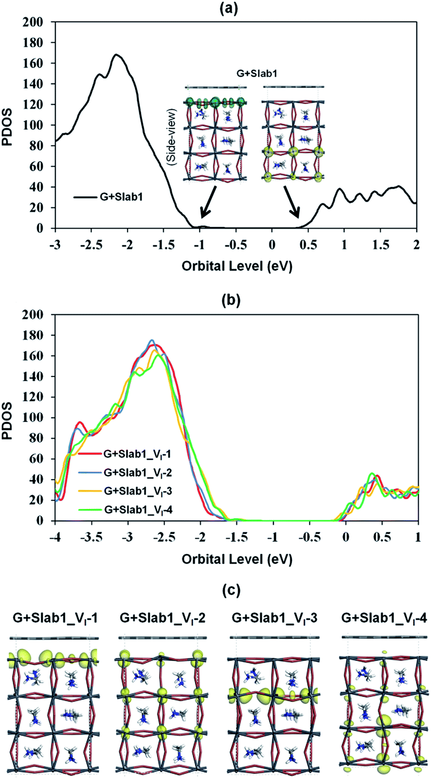 | ||
| Fig. 8 Calculated partial density of states (PDOS) of MAPbI3 in the graphene + MAPbI3 hybrids: (a) defect-free and (b) VI-containing models, and (c) the orbital shape corresponds to the conduction band edges of MAPbI3 (isovalue: 0.015 a.u.). | ||
3.2. MAPbI3 with a Pb vacancy
A single Pb vacancy (VPb) is another defect which might exist in MAPbI3. When a neutral Pb atom is removed to form a VPb in the bulk, the DFT optimization showed that the six neighboring I atoms change their positions slightly as shown in Fig. S4 of the ESI,† but the change is not so appreciable: the average distance between the two adjacent I atoms is 4.404 Å (change of −2.7%), which is close to that in the perfect crystal (4.528 Å). The calculated DOS suggests that the VPb in bulk MAPbI3 acts as a shallow acceptor because some holes are generated in the valence band as seen in Fig. S5 of the ESI.† This p-type characteristic has already been pointed out by Kim et al.35Concerning slab models having a VPb, two types of configurations are possible: the VPb may appear on the surface or in the bulk as depicted in Fig. 9(b). Here, these models are called Slab1_VPb-1 and Slab1_VPb-2, respectively. Although they have a common defect, i.e. VPb, the optimized structures are significantly different as shown in the upper panel of Fig. 9(b): removal of a surface Pb atom (Slab1_VPb-1) leads to the formation of an I–I dimer having an interatomic distance of 2.778 Å. Such a short I–I distance was also obtained in the larger slab model (Slab4) as shown in Fig. S3(b).† In contrast, in Slab1_VPb-2, the inner VPb produces 6 dangling I atoms without any dimerization of the two neighboring I atoms, namely, the structural feature inside the MAPbI3 slab is essentially similar to that in the bulk.
 | ||
| Fig. 9 (a) Defect-free and (b) VPb-containing defective MAPbI3 slabs. | ||
The DOSs of Slab1_VPb-1 and Slab1_VPb-2 also show a marked difference (Fig. 10(b) and (c)). After geometry optimization, the former has a discrete mid-gap level, while the latter does not. The DOS spectra of the two systems before optimization (Fig. 10(a)) indicate that, without structural reorganization, the two spectra of the valence band are almost identical. After the geometry optimization, the top region of the valence band of Slab1_VPb-1 splits to generate the discrete level pointed out above. After the band splitting, the valence band after optimization becomes completely filled with electrons. It is interesting to note that the DOS of the conduction band does not change its shape even after geometry optimization. This supports the view that the mid-gap level originated from the valence band.
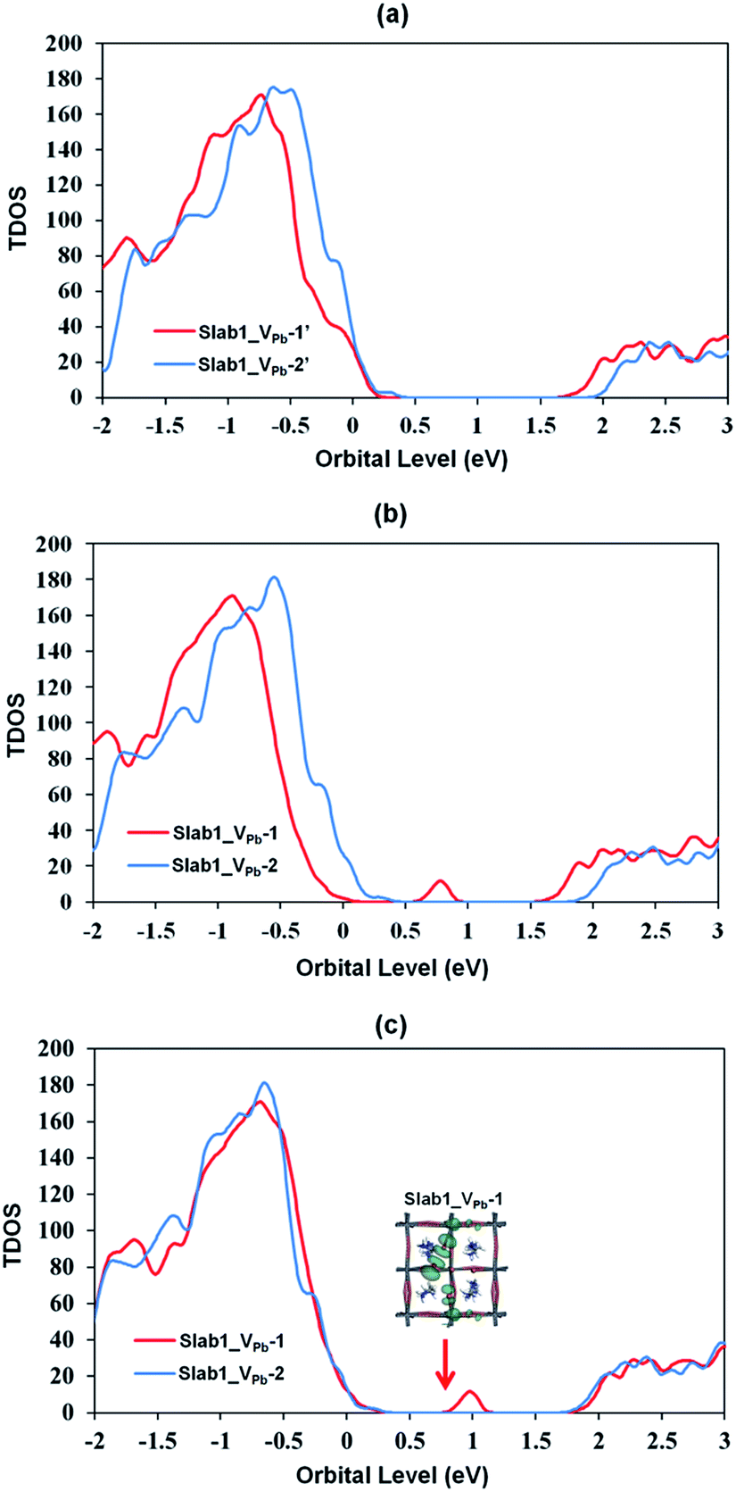 | ||
| Fig. 10 Calculated total density of states (TDOS) of the VPb-containing MAPbI3 slab models (a) before geometry optimization, (b) after geometry optimization, and (c) after geometry optimization where the valence band tops of all the defective slab models were adjusted to the same level. The inset in (c) indicates the orbital shape. | ||
The change in the DOS of Slab1_VPb-1 implies that the defect center would be positively charged. The calculated Hirshfeld charge shows that the net charge of the dimerized I2 center is −0.52 (see Table 2) which is much smaller than that of the defect-free system. On the surface of the latter, the total net charge of two surface I atoms is −0.91: 0.39 electrons are taken from the two I atoms and are transferred to the other region of the crystal (see Fig. S14 of the ESI†). This indicates that the VPb acts as a hole trap because the I2 dimer formation is possible though bonding interaction between the two adjacent I atoms as shown in Fig. 11.
| Structure | Graphene | Slab1_VPb | |
|---|---|---|---|
| Dangling I atomsa | The rest in total | ||
| a Sum of five (or six) iodine atoms in G + Slab1_VPb-1 (or G + Slab1_VPb-2). b Calculated from the average charge (−0.18 e per I atom) and the number of dangling I atoms. −0.91 e (−1.09 e) is for the five (six) dangling atoms. | |||
| G + Slab1 | −0.20 | (−0.91/−1.09)b | (+0.91/+1.09) |
| G + Slab1_VPb-1 | +0.14 | −0.78(−0.52) | +0.64(+0.52) |
| G + Slab1_VPb-2 | +0.07 | −0.99(−0.97) | +0.92(+0.97) |
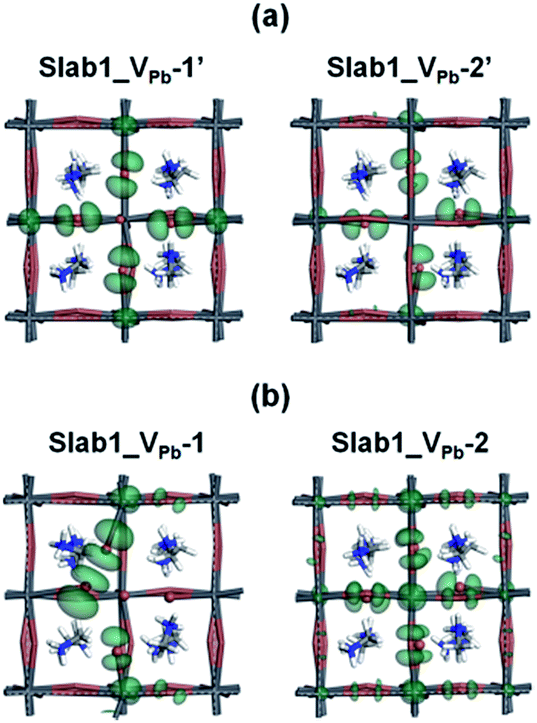 | ||
| Fig. 11 The orbital shape of the valence band edges (isovalue: 0.015 a.u.) of the VPb-containing MAPbI3 slab models (a) before and (b) after geometry optimization. | ||
It seems reasonable to expect that further hole doping would result in I2 dimer formation even in the inner region (Slab1_VPb-2) as has been observed for the VI. Unexpectedly, additional hole doping did not result in dimer formation in this inner defect model as shown in Fig. S16(d) of the ESI.† The hole trapping character of the VPb also suggests that electron doping into Slab1_VPb-1 should break the dimer. The optimized geometries of such systems (singly and doubly electron-doped ones) clearly show the elongation of the I–I distance as seen in Fig. S15 of the ESI.† This observation also justifies the hole-doped character of the surface I–I dimer.
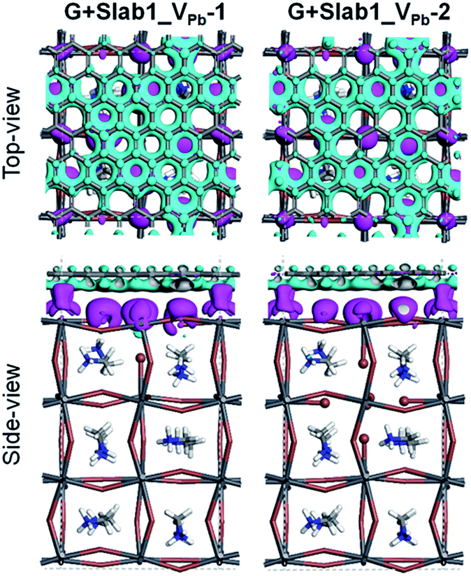
Since we have observed substantial effect of graphene coating on the electronic structure of the defective MAPbI3, the corresponding hybrid structures represented as G + Slab1_VPb-1 and G + Slab1_VPb-2 were also investigated. The optimized structures in Fig. 12 (see also Fig. S17 of the ESI†) clearly show that, in this hybrid system, the I2 dimer does not form on the surface. The calculated PDOS for the MAPbI3 moiety (Fig. 13) is similar to that of the bulk: no mid-gap level appears even in Slab1_VPb-1. Therefore, we conclude that graphene has a healing effect even for removing the hole trap.
 | ||
| Fig. 12 (a) Defect-free and (b) VPb-containing defective graphene + MAPbI3 hybrids. | ||
 | ||
| Fig. 13 (a) Calculated partial density of states (PDOS) of MAPbI3 in the VPb-containing graphene + MAPbI3 hybrids, and (b) the orbital shape of the valence band edges of MAPbI3 (isovalue: 0.015 a.u.). | ||
In order to analyse the driving force for the cleavage of the I–I dimer by graphene, we investigated the Hirshfeld charge of the pristine perovskites and hybrid structures and the results are tabulated in Table 2. We see that the Hirshfeld charge of graphene in the hybrids is positive (+0.14 e and +0.07 e in G + Slab1_VPb-1 and G + Slab1_VPb-2, respectively). This is different from the electron-accepting character of graphene (−0.20 e, Table 2) in the defect-free system, which may result from the p-type doping with the VPb as mentioned. The electron-donating character is also proved by the calculated EDD distributions shown in Fig. 14: the electrons are extracted from the attached graphene layer to the VPb-containing MAPbI3.
 | ||
| Fig. 14 Electron density difference of the VPb-containing graphene + MAPbI3 hybrids (isovalue: 0.003 a.u.). Purple and cyan represent accumulation and depletion of electrons, respectively. | ||
The Hirshfeld charge distribution clarifies the role of the graphene on the surface. The sum of the net charges of the five dangling I atoms in Slab1_VPb-1 is −0.52 e, while it becomes −0.78 e after graphene coating (see also Fig. S14 and S18 for details†). In the difference (0.26 e), 0.14 e are provided by graphene, and 0.12 e are transferred from the rest of the crystal. Therefore, graphene plays two roles: one is to provide electrons to the hole-trapping site, and the other is to reorganize the charge distribution in the crystal. Through comparison with Slab1_VPb-2, we find that the surface vacancy always has a larger influence on charge redistribution.
3.3. MAPbI3 with a MA vacancy
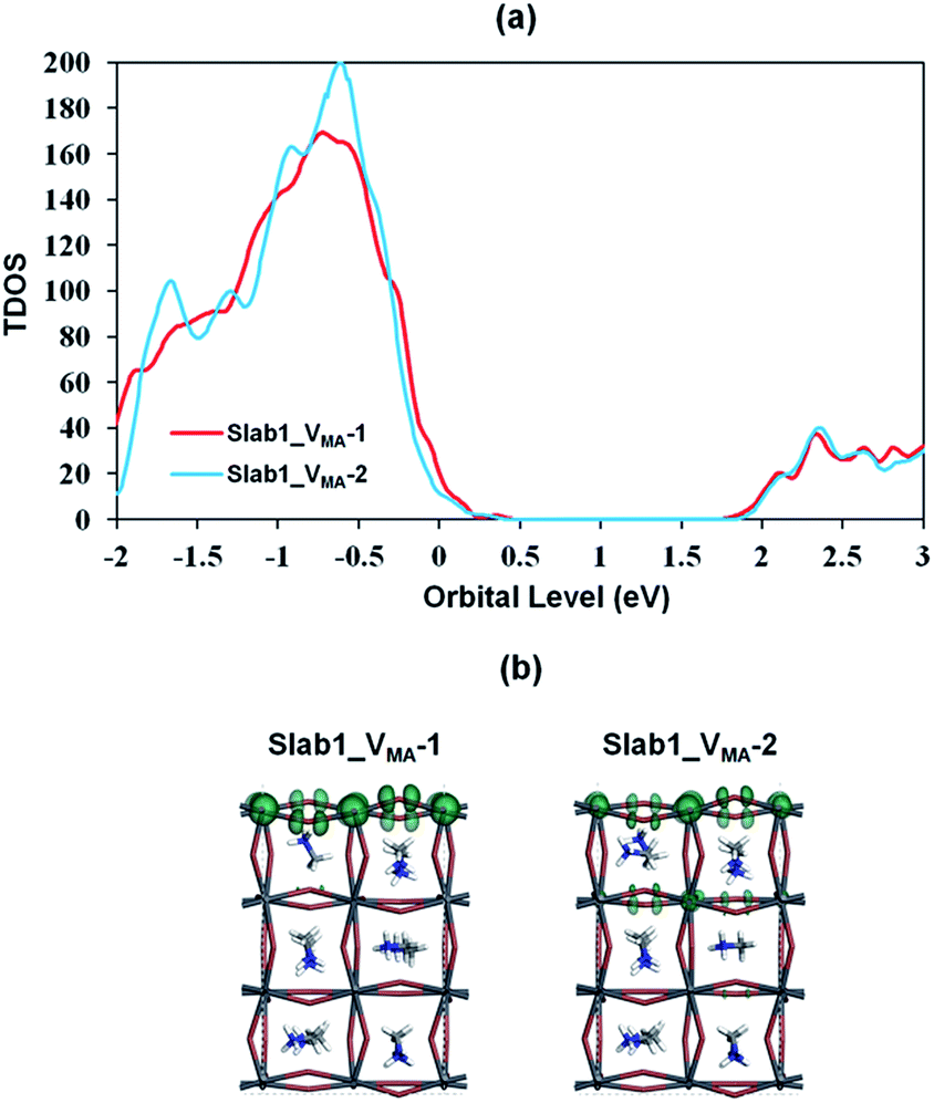
We also investigated the MA vacancy (VMA) in MAPbI3. The calculated DOS (Fig. S5(d) of the ESI†) shows that the VMA in the bulk MAPbI3 acts as a p-type doping defect and produces a shallow-level defect near the band edge. This feature is similar to that of the VPb in the bulk MAPbI3 model.For the perovskite slabs with a single VMA, two defective models with different VMA locations were calculated (Fig. 15). The calculated DOS in Fig. 16 reveals that the VMA of MAPbI3 slabs always shows a shallow-level defect near the band edge. Therefore, it can be concluded that the trap center in perovskites forms only when the PbI6 octahedral unit is deformed (i.e. VI or VPb).
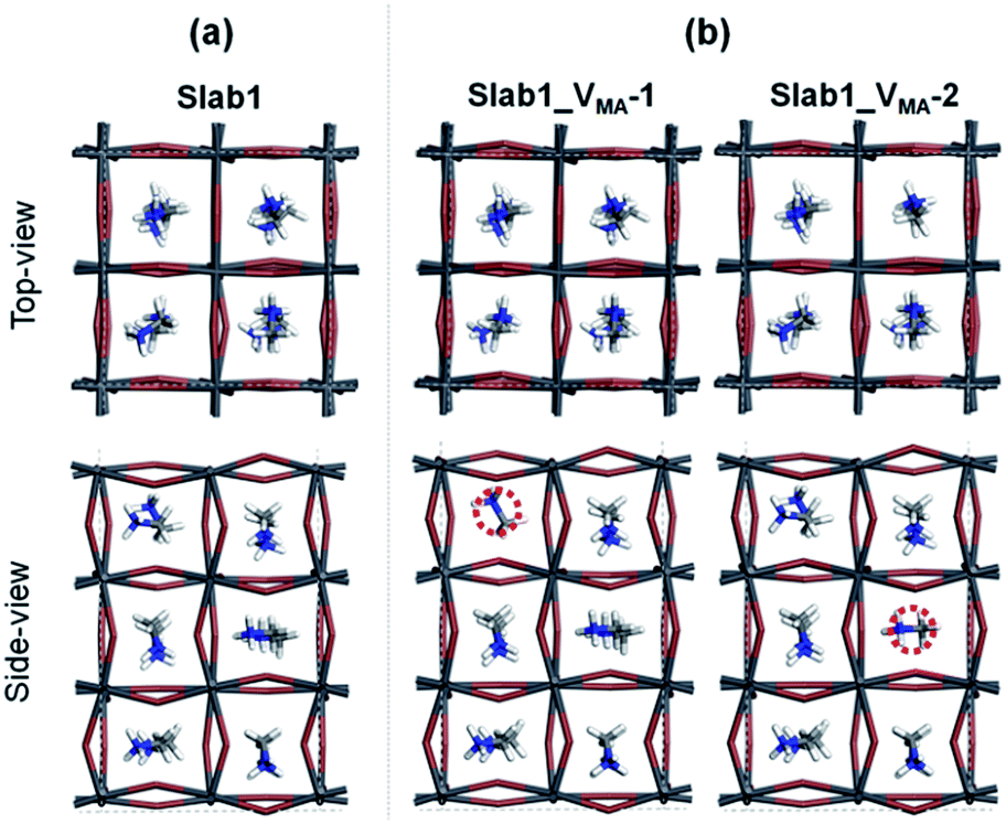 | ||
| Fig. 15 (a) Defect-free and (b) VMA-containing defective MAPbI3 slabs. | ||
 | ||
| Fig. 16 (a) Calculated total density of states (TDOS) of VMA-containing MAPbI3, and (b) the orbital shape of the valence band edges of MAPbI3 (isovalue: 0.015 a.u.). | ||
In contrast, the A-site single vacancy, e.g. VMA, shows a high defect tolerance character no matter how the vacancy resides around the surface or in the bulk position. In the presence of graphene, a compressed PbI2 surface is observed (Fig. 17) and the modification in the PDOS of defective MAPbI3 is insignificant (Fig. 18). In addition, similar to the defective perovskite with a VPb, the cationic defect and excess hole doping results in an electron deficient character of the perovskite. Graphene acts as an electron donor in the hybrid structure, which can be proved by the Hirshfeld charge (+0.10 and +0.09 e of graphene in G + Slab1_VMA-1 and G + Slab1_VMA-2, respectively, Table S5 of the ESI†) and the visualized EDD shown in Fig. 19.
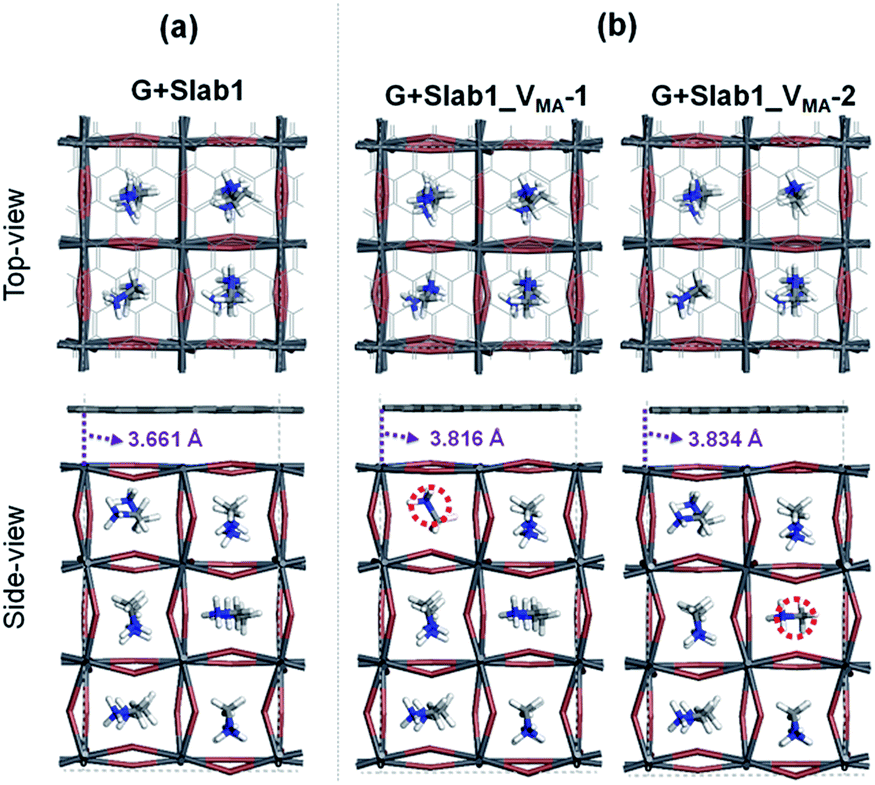 | ||
| Fig. 17 (a) Defect-free and (b) VMA-containing defective graphene + MAPbI3 hybrids. | ||
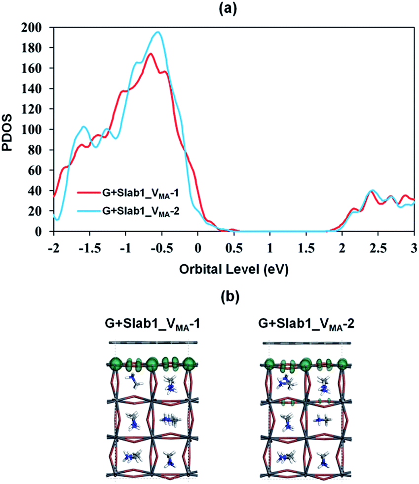 | ||
| Fig. 18 (a) Calculated partial density of states (PDOS) of MAPbI3 in the VMA-containing graphene + MAPbI3 hybrids, and (b) the orbital shape of the valence band edges of MAPbI3 (isovalue: 0.015 a.u.). | ||
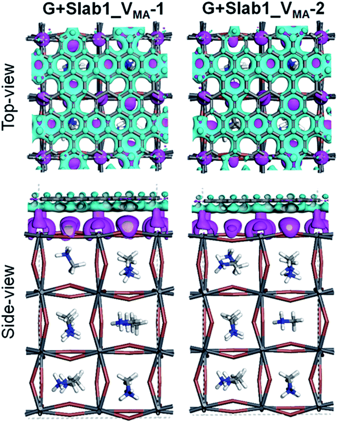 | ||
| Fig. 19 Electron density difference of the VMA-containing graphene + MAPbI3 hybrids (isovalue: 0.003 a.u.). Purple and cyan represent accumulation and depletion of electrons, respectively. | ||
3.4. Molecules showing the healing effect
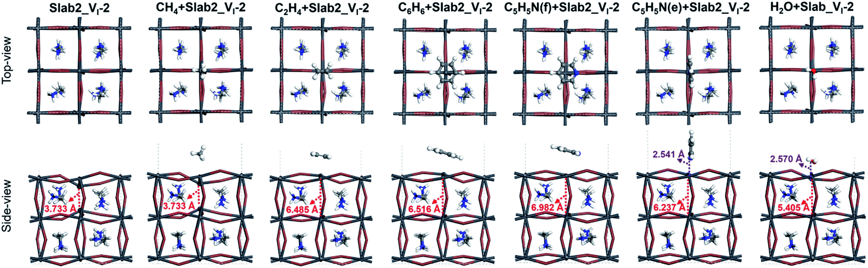
So far, we have shown that graphene has a healing effect that suppresses electron- and hole-trapping due to I and Pb vacancies on the surface of MAPbI3. It seems interesting to investigate what other chemicals would also show the healing effect. Since aromatic π electrons can interact with ions, aromatic compounds would be an alternative to graphene. It is also interesting to investigate non-aromatic unsaturated hydrocarbons in order to highlight the importance of π electrons. Small molecules forming Werner complexes on the Pb center are also interesting. In experiments, coating with organic molecules (such as C5H5N) has also been investigated and has been shown to improve the device performance.56Herein CH4, C2H4, C6H6, and C5H5N were selected as the first candidates for the experiments. In order to reduce computational cost, here we employed a smaller MAPbI3 slab (Fig. S1 of the ESI,† labelled Slab2) to study the molecular adsorption. Note that the Slab2 model showed similar defective properties (Pb or I dimer formation around the surface and the corresponding trap-level defects) and the healing effect of graphene (Fig. S19–S23 of the ESI†). Here Slab2_VI-2 with a Pb–Pb dimer and Slab2_VPb-1 with an I–I dimer (Fig. S19 of the ESI†) were employed as defective perovskite models.
In the case of Slab2_VI-2 with a dimerized Pb segment, the Pb–Pb dimer was removed when C2H4, C6H6, or C5H5N was adsorbed onto the surface (see Fig. 20). The calculated DOS further confirmed that the deep-level defects of those defective MAPbI3 vanished (Fig. 21). It should be noted that the dimerized Pb was always broken when the configuration of C5H5N is face-on (C5H5N(f) + Slab2_VI-2) or edge-on (C5H5N(e) + Slab2_VI-2). In the case of C2H4, C6H6, and C5H5N with a face-on orientation, the calculated Hirshfeld charge on the dimerized Pb–Pb dimer is reduced by 0.10, 0.13, and 0.08 e, respectively, giving rise to the charge delocalization and the cleavage of the Pb2 dimer (Fig. 21 and S24 of the ESI†). On the other hand, for the end-on C5H5N, the molecule is adsorbed via lone-pair interactions between N and the Pb on the defective site (4-coordinated originally). The N–Pb distance is as short as 2.541 Å. Consequently, this 4-coordinated Pb becomes 5-coordinated which is the same as that observed for other Pb atoms on the surface without defects. Therefore, we see that when the electron distribution is delocalized the dimer formation is suppressed.
 | ||
| Fig. 20 Defective MAPbI3 slabs (Slab2_VI-2) and the corresponding molecule + MAPbI3 hybrids. | ||
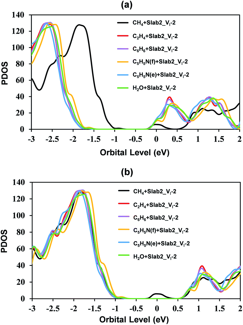 | ||
| Fig. 21 Calculated partial density of states (PDOS) of the molecule + VI-containing MAPbI3 (Slab2_VI-2) hybrids. (a) presents the original data and (b) presents the adjusted data in which the valence band tops of all the slab models were adjusted to the same level for clarity. | ||
Motivated by the observations, we further studied the H2O + Slab2_VI-2 (Fig. 20) hybrid. As expected, because of a similar lone pair interaction between the O of H2O and the Pb on the defective site, the attached H2O can also disrupt the Pb–Pb dimer with an elongated distance of 5.405 Å. Therefore, water molecules are effective in removing the deep-level defects caused by Pb–Pb dimers (Fig. 21 and S24 of the ESI†), which can be used to explain the previous experimental evidence, that is, the sprayed water molecules result in decreased defect density and improved device efficiencies.57,58
So far, we have assumed that the perovskite layer was prepared under PbI2-rich conditions because a stronger interaction with graphene is expected. This is also justified by the experiment suggesting that the PbI2-terminated MAPbI3 provides an improved photo-carrier transport and higher performance.59–62 However, the existence of the MAI-terminated surface cannot be excluded since the surface composition of the perovskite can be modulated by synthesis procedures. In addition, the MAI layer at the grain boundaries of MAPbI3 was reported as a healing layer to improve the carrier lifetime and suppress the charge recombination at the interfaces.63 Therefore we also investigated a MAI-terminated perovskite slab model with a single VI (Fig. S25 of the ESI†). The optimized geometry showed that the Pb–Pb dimer does not form and has a large interatomic distance of 6.980 Å (Fig. S26 and S27 of the ESI†) in the Slab5_VI-4 model which is comparable to that in the Slab1_VI_2 model. This result indicates that the surface with MAI would not have electron traps. This is consistent with the previous conclusions experimentally obtained.59–62
For the defective MAPbI3 with an I–I dimer, which is predicted for the system with the surface VPb, the present calculation predicts that the selected molecules or MAI does not give the healing effect. This may be due to the poor electron donating abilities of these species: the dimerized I2 still exists upon coordination of these molecules even after adsorption (Fig. S26 and S28 of the ESI†). Therefore, we can conclude that graphene exhibits healing effects on electron- and hole-traps due to single vacancies. This implies that the introduction of the graphene layer would be beneficial to both surfaces of metal halide perovskite layers connected to electron- and hole-transporting materials. The present results also imply that the use of π-conjugated compounds like fullerene and spiro-OMeTAD would be very reasonable because both of them would also have a healing effect to remove carrier traps at the interface in perovskite solar cells.
4 Conclusions
In this study, we have investigated the geometries and electronic structures of the surfaces of the MAPbI3 perovskite compound with single vacancies by using first-principles calculations. We have also studied the impact of surface fabrication using graphene because energy conversion devices using this material have a multi-layered structure.The present computation predicts that Pb and I vacancies beneath the surface can function as carrier traps. The appearance of the mid-gap levels near the vacancies is due to the formation of the I–I and Pb–Pb dimers, respectively. This characteristic of the defective material is considered to degrade the performance of energy conversion devices using MAPbI3. This feature would be quite unique only in the surface region: in the bulk, such dimers would not form, as suggested by Zhang et al.8 The MA vacancy is considered to be harmless in electronic devices.
Through the investigation of the surface fabrication using graphene, we have found that the undesirable I–I and Pb–Pb dimers do not form in the stable geometries in the defective systems. This is because charge localization at a Pb/I single vacancy is suppressed by graphene. This characteristic indicates that graphene has a “healing effect” against carrier trapping by the vacancy. This healing effect has also been predicted for surface coating with unsaturated hydrocarbons, but graphene is more beneficial because it is effective in eliminating any kind of carrier trapping. The origin of the healing effect would be electronic interaction on the surface providing electrons/holes to suppress the formation of the carrier traps. It also plays a role in preventing charge localization at the trapping sites around a single vacancy.
Conflicts of interest
There are no conflicts to declare.Acknowledgements
This research was financially supported by the New Energy and Industrial Technology Development Organization (NEDO) project and by a Grant-in-Aid for Scientific Research on Innovative Areas “π-Figuration” (JSPS KAKENHI 26102015 for M. S.).Notes and references
- M. R. Filip, G. E. Eperon, H. J. Snaith and F. Giustino, Nat. Commun., 2014, 5, 5757 CrossRef CAS PubMed.
- W.-J. Yin, T. Shi and Y. Yan, Adv. Mater., 2014, 26, 4653 CrossRef CAS PubMed.
- G. Xing, N. Mathews, S. Sun, S. S. Lim, Y. M. Lam, M. Grätzel, S. Mhaisalkar and T. C. Sum, Science, 2013, 342, 344 CrossRef CAS PubMed.
- A. Kojima, K. Teshima, Y. Shirai and T. Miyasaka, J. Am. Chem. Soc., 2009, 131, 6050 CrossRef CAS PubMed.
- NREL, Best Research-Cell Efficiencies, https://www.nrel.gov/pv/assets/images/efficiency-chart.png.
- W. Shockley and H. J. Queisser, J. Appl. Phys., 1961, 32, 510 CrossRef CAS.
- J. M. Ball and A. Petrozza, Nat. Energy, 2016, 1, 16149 CrossRef CAS.
- M. L. Agiorgousis, Y. Y. Sun, H. Zeng and S. Zhang, J. Am. Chem. Soc., 2014, 136, 14570 CrossRef CAS PubMed.
- T. Tachikawa, I. Karimata and Y. Kobori, J. Phys. Chem. Lett., 2015, 6, 3195 CrossRef CAS.
- Y. Yamada, T. Yamada, A. Shimazaki, A. Wakamiya and Y. Kanemitsu, J. Phys. Chem. Lett., 2016, 7, 1972 CrossRef CAS PubMed.
- T. S. Sherkar, C. Momblona, L. Gil-Escrig, H. J. Bolink and L. J. A. Koster, Adv. Energy Mater., 2017, 7, 1602432 CrossRef.
- Y. Shao, Y. Fang, T. Li, Q. Wang, Q. Dong, Y. Deng, Y. Yuan, H. Wei, M. Wang, A. Gruverman, J. Shielda and J. Huang, Energy Environ. Sci., 2016, 9, 1752 CAS.
- X. Wu, M. T. Trinh, D. Niesner, H. Zhu, Z. Norman, J. S. Owen, O. Yaffe, B. J. Kudisch and X.-Y. Zhu, J. Am. Chem. Soc., 2015, 137, 2089 CrossRef CAS PubMed.
- J. Kang and L.-W. Wang, J. Phys. Chem. Lett., 2017, 8, 489 CrossRef CAS PubMed.
- Y. Liu, Z. Yang, D. Cui, X. Ren, J. Sun, X. Liu, J. Zhang, Q. Wei, H. Fan, F. Yu, X. Zhang, C. Zhao and S. Liu, Adv. Mater., 2015, 27, 5176 CrossRef CAS PubMed.
- Y. Shao, Z. Xiao, C. Bi, Y. Yuan and J. Huang, Nat. Commun., 2014, 5, 5784 CrossRef CAS PubMed.
- J. Xu, A. Buin, A. H. Ip, W. Li, O. Voznyy, R. Comin, M. Yuan, S. Jeon, Z. Ning, J. J. McDowell, P. Kanjanaboos, J. P. Sun, X. Lan, L. N. Quan, D. H. Kim, I. G. Hill, P. Maksymovych and E. H. Sargent, Nat. Commun., 2015, 6, 7081 CrossRef CAS PubMed.
- C.-H. Chiang and C.-G. Wu, Nat. Photonics, 2016, 10, 196 CrossRef CAS.
- A. Abate, M. Saliba, D. J. Hollman, S. D. Stranks, K. Wojciechowski, R. Avolio, G. Grancini, A. Petrozza and H. J. Snaith, Nano Lett., 2014, 14, 3247 CrossRef CAS PubMed.
- N. K. Noel, A. Abate, S. D. Stranks, E. S. Parrott, V. M. Burlakov, A. Goriely and H. J. Snaith, ACS Nano, 2014, 8, 9815 CrossRef CAS PubMed.
- F. Wang, W. Geng, Y. Zhou, H. H. Fang, C. J. Tong, M. A. Loi, L. M. Liu and N. Zhao, Adv. Mater., 2016, 28, 9986 CrossRef CAS PubMed.
- S. Ye, H. Rao, Z. Zhao, L. Zhang, H. Bao, W. Sun, Y. Li, F. Gu, J. Wang, Z. Liu, Z. Bian and C. Huang, J. Am. Chem. Soc., 2017, 139, 7504 CrossRef CAS PubMed.
- Q. Chen, H. Zhou, T. B. Song, S. Luo, Z. Hong, H. S. Duan, L. Dou, Y. Liu and Y. Yang, Nano Lett., 2014, 14, 4158 CrossRef CAS PubMed.
- T. S. Sherkar, C. Momblona, L. Gil-Escrig, J. Ávila, M. Sessolo, H. J. Bolink and L. J. A. Koster, ACS Energy Lett., 2017, 2, 1214 CrossRef CAS PubMed.
- J.-S. Yeo, C.-H. Lee, D. Jang, S. Lee, S. M. Jo, H.-I. Joh and D.-Y. Kim, Nano Energy, 2016, 30, 667 CrossRef CAS.
- Z. Zhu, J. Ma, Z. Wang, C. Mu, Z. Fan, L. Du, Y. Bai, L. Fan, H. Yan, D. L. Phillips and S. Yang, J. Am. Chem. Soc., 2014, 136, 3760 CrossRef CAS PubMed.
- J. T.-W. Wang, J. M. Ball, E. M. Barea, A. Abate, J. A. Alexander-Webber, J. Huang, M. Saliba, I. Mora-Sero, J. Bisquert, H. J. Snaith and R. J. Nicholas, Nano Lett., 2014, 14, 724 CrossRef CAS PubMed.
- G. S. Han, Y. H. Song, Y. U. Jin, J.-W. Lee, N.-G. Park, B. K. Kang, J.-K. Lee, I. S. Cho, D. H. Yoon and H. S. Jung, ACS Appl. Mater. Interfaces, 2015, 7, 23521 CAS.
- Q. Luo, Y. Zhang, C. Liu, J. Li, N. Wang and H. Lin, J. Mater. Chem. A, 2015, 3, 15996 CAS.
- W. Li, H. Dong, X. Guo, N. Li, J. Li, G. Niu and L. Wang, J. Mater. Chem. A, 2014, 2, 20105 CAS.
- K. Yan, Z. Wei, J. Li, H. Chen, Y. Yi, X. Zheng, X. Long, Z. Wang, J. Wang, J. Xu and S. Yang, Small, 2015, 11, 2269 CrossRef CAS PubMed.
- Y. Jiao, F. Ma, G. Gao, H. Wang, J. Bell, T. Frauenheim and A. Du, RSC Adv., 2015, 5, 82346 RSC.
- Z. Wu, S. Bai, J. Xiang, Z. Yuan, Y. Yang, W. Cui, X. Gao, Z. Liu, Y. Jin and B. Sun, Nanoscale, 2014, 6, 10505 RSC.
- J. Bouclé and N. Herlin-Boime, Synth. Met., 2016, 222, 3 CrossRef.
- J. Kim, S.-H. Lee, J. H. Lee and K. H. Hong, J. Phys. Chem. Lett., 2014, 5, 1312 CrossRef CAS PubMed.
- J. Haruyama, K. Sodeyama, L. Han and Y. Tateyama, J. Phys. Chem. Lett., 2014, 5, 2903 CrossRef CAS PubMed.
- J. Kang and L.-W. Wang, J. Phys. Chem. Lett., 2017, 8, 489 CrossRef CAS PubMed.
- W.-J. Yin, T. Shi and Y. Yan, Appl. Phys. Lett., 2014, 104, 063903 CrossRef.
- M. H. Du, J. Mater. Chem. A, 2014, 2, 9091 CAS.
- J. Kim, S.-H. Lee, J. H. Lee and K. H. Hong, J. Phys. Chem. Lett., 2014, 5, 1312 CrossRef CAS PubMed.
- A. Buin, P. Pietsch, J. Xu, O. Voznyy, A. H. Ip, R. Comin and E. H. Sargent, Nano Lett., 2014, 14, 6281 CrossRef CAS PubMed.
- W.-J. Yin, T. Shi and F. Yan, J. Phys. Chem. C, 2015, 119, 5253 CAS.
- J. Kim, C.-H. Chung and K.-H. Hong, Phys. Chem. Chem. Phys., 2016, 18, 27143 RSC.
- M.-H. Du, J. Phys. Chem. Lett., 2015, 6, 1461 CrossRef CAS PubMed.
- H. Uratani and K. Yamashita, J. Phys. Chem. Lett., 2017, 8, 742 CrossRef CAS PubMed.
- L. Wei, W. Ma, C. Lian and S. Meng, J. Phys. Chem. C, 2017, 121, 5905 CAS.
- K. Refson, P. R. Tulip and S. J. Clark, Phys. Rev. B: Condens. Matter Mater. Phys., 2006, 73, 155114 CrossRef.
- S. J. Clark, M. D. Segall, C. J. Pickard, P. J. Hasnip, M. J. Probert, K. Refson and M. C. Payne, Z. Kristallogr., 2005, 220, 567 CAS.
- J. P. Perdew, K. Burke and M. Ernzerhof, Phys. Rev. Lett., 1996, 77, 3865 CrossRef CAS PubMed.
- A. Tkatchenko and M. Scheffler, Phys. Rev. Lett., 2009, 102, 073005 CrossRef PubMed.
- D. Vanderbilt, Phys. Rev. B: Condens. Matter Mater. Phys., 1990, 41, 7892 CrossRef.
- J. Lian, Q. Wang, Y. Yuan, Y. Shao and J. Huang, J. Mater. Chem. A, 2015, 3, 9146 CAS.
- Y. Kawamura, H. Mashiyama and K. Hasebe, J. Phys. Soc. Jpn., 2002, 71, 1694 CrossRef CAS.
- C. C. Stoumpos, C. D. Malliakas and M. G. Kanatzidis, Inorg. Chem., 2013, 52, 9019 CrossRef CAS PubMed.
- G. Volonakis and F. Giustino, J. Phys. Chem. Lett., 2015, 6, 2496 CrossRef CAS PubMed.
- D. W. de Quilettes, S. M. Vorpahl, S. D. Stranks, H. Nagaoka, G. E. Eperon, M. E. Ziffer, H. J. Snaith and D. S. Ginger, Science, 2015, 348, 683 CrossRef CAS PubMed.
- Q.-Q. Ge, J. Ding, J. Liu, J.-Y. Ma, Y.-X. Chen, X.-X. Gao, L.-J. Wan and J.-S. Hu, J. Mater. Chem. A, 2016, 4, 13458 CAS.
- W. Zhou, Y. Zhao, C. Shi, H. Huang, J. Wei, R. Fu, K. Liu, D. Yu and Q. Zhao, J. Phys. Chem. C, 2016, 120, 4759 CAS.
- J. Haruyama, K. Sodeyama, L. Han and Y. Tateyama, Acc. Chem. Res., 2016, 49, 554 CrossRef CAS PubMed.
- T. J. Jacobsson, J.-P. Correa-Baena, E. H. Anaraki, B. Philippe, S. D. Stranks, M. E. F. Bouduban, W. Tress, K. Schenk, J. Teuscher, J.-E. Moser, H. Rensmo and A. Hagfeldt, J. Am. Chem. Soc., 2016, 138, 10331 CrossRef CAS PubMed.
- J.-H. Im, I.-H. Jang, N. Pellet, M. Grätzel and N.-G. Park, Nat. Nanotechnol., 2014, 9, 927 CrossRef CAS PubMed.
- R. Lindblad, D. Bi, B.-w. Park, J. Oscarsson, M. Gorgoi, H. Siegbahn, M. Odelius, E. M. J. Johansson and H. Rensmo, J. Phys. Chem. Lett., 2014, 5, 648 CrossRef CAS PubMed.
- D.-Y. Son, J.-W. Lee, Y. J. Choi, I.-H. Jang, S. Lee, P. J. Yoo, H. Shin, N. Ahn, M. Choi, D. Kim and N.-G. Park, Nat. Energy, 2016, 1, 16081 CrossRef CAS.
Footnote |
| † Electronic supplementary information (ESI) available: Detailed information on the geometries, energies, charge distributions, and density of states of relevant structures. See DOI: 10.1039/c7sc04837h |
| This journal is © The Royal Society of Chemistry 2018 |