 Open Access Article
Enhanced visible light absorption performance of SnS2 and SnSe2 via surface charge transfer doping†
F. F. Xia *a,
F. L. Yanga,
J. Hua,
C. Z. Zhenga,
H. B. Yi
 *b and
J. H. Sun
 *a
*a
aSchool of Chemical and Environmental Engineering, Jiangsu University of Technology, Changzhou 213001, Jiangsu, P. R. China. E-mail: ffxia@jsut.edu.cn; sunjh@jsut.edu.cn
bState Key Laboratory of Chemo/Biosensing and Chemometrics, College of Chemistry and Chemical Engineering, Hunan University, Changsha 410082, Hunan, P. R. China. E-mail: hbyi@hnu.edu.cn
First published on 4th December 2018
Abstract
The layered two-dimensional (2D) SnS2 and SnSe2 have received intensive attention due to their sizable band gaps and potential properties. However, it has been shown that the visible light absorption of SnS2 and SnSe2 are restricted as photocatalysts and light-harvesting material absorbers for water splitting and high-performance optoelectronic devices. Herein, to enhance the visible light absorption performance of SnS2 and SnSe2, we performed a systematic investigation on tuning the electronic and optical properties of monolayers SnS2 and SnSe2 via surface charge transfer doping (SCTD) with the adsorption of molybdenum trioxide (MoO3) and potassium (K) as surface dopants based on density functional theory. Our calculations reveal that MoO3 molecules and K atoms can draw/donate electrons from/to SnS2 and SnSe2 as acceptors and donors, respectively. The adsorption of MoO3 molecules introduces a new flat impurity state in the gap of the monolayers SnS2/SnSe2, and the Fermi level moves correspondingly to the top of valence band, resulting in a p-type doping of the monolayer SnS2/SnSe2. With the adsorption of K atoms, the electrons can transfer from K atoms to the monolayer of SnS2 and SnSe2, making K an effective electron-donating dopant. Meanwhile, the bandgaps of monolayers SnS2 and SnSe2 decrease after the MoO3 and K doping, which leads to the appearance of appreciable new absorption peaks at around ∼650/480 and ∼600/680 nm, respectively, and yielding an enhanced visible light absorption of SnS2 and SnSe2. Our results unveil that SCTD is an effective way to improve the photocatalytic and light-harvesting performance of SnS2 and SnSe2, broadening their applications in splitting water and degrading environmental pollutants under sunlight irradiation.
Introduction
Since Fujishima and Honda discovered the photocatalytic splitting of water on TiO2 electrodes in 1972,1 the TiO2 nanostructures have attached much research attention as photocatalysts due to its promising applications in the efficient conversion of sunlight to environmentally friendly renewable energy and the treatment of environmental pollution.2,3 However, the photoreaction efficiency of TiO2 is severely limited by its large intrinsic band gap (e.g., for the anatase phase, 3.20 eV), which makes it impossible to utilize the visible light of solar spectrum.4As one type of the two-dimensional (2D) layered chalcogenide materials (LCMs), tin dichalcogenides SnX2 (X = S and Se) have potential performance such as low toxicity, easy availability and high chemical and thermal stability with a hexagonal crystal structure of the type CdI2,5,6 making their wide range of applications in gas sensing,7,8 anode materials,9,10 photochemical reactions,11–19 and optoelectronic devices.20–22 Of particular note is that, due to their high specific surface area, ultrathin SnS2 and SnSe2 are widely investigated as photocatalysts and light-harvesting material absorbers for photochemical reactions11–26 and optoelectronic devices,27–29 respectively. For instance, freestanding SnS2 single-layers with three atom thickness were first synthesized through a convenient and scalable liquid exfoliation strategy, offering an excellent platform to achieve efficient visible-light water splitting, which can approach a higher visible-light conversion efficiency (38.7%) than that of bulk phase (2.33%).11 Also, it is reported that ultrathin SnS2 nanosheets are utilized as solar-driven photocatalyst, but there is quite challenging to explore a material with suitable band alignment using SnS2 nanomaterials for photocatalytic hydrogen generation.14 Nevertheless, the theoretical perspective showed that the optical band gap lied within the range of visible light,15 implying a significant fraction of solar light can be harvested by single-layer SnS2, but the overall water splitting cannot spontaneously take place on the SnS2 nanosheets because the conduction band minimum (CBM) is insufficient to drive the hydrogen evolution. Yu et al. also discovered SnS2 nanosheets exhibit the highest photocatalytic hydrogen generation ability, which may be attributed to narrower optical band gap and unique 2D morphology.16 In addition, Mukhokosi et al.28 have observed that the band gap of SnSe2 depends on thin film thickness, that is ∼2.04 eV for 50 nm thick film similar to that of monolayers, whereas it is approximately 1.2 eV for the 1200 nm thick film similar to that of bulk phase. And the IR photodetection response of SnSe2 demonstrates a sensitivity of ∼3% for a 1000 nm thick film (bulk phase), but the sensitivity is 90.4% for 140 nm thick film (monolayers) at 100 mW cm−2, suggesting the SnSe2 thin film can be explored as an excellent material for photodetection. Overall, all these results show that 2D layered SnS2 and SnSe2 are restricted as photocatalysts and light-harvesting material absorbs for water splitting and high-performance optoelectronic devices, respectively. Therefore, in order to make effective use of the visible light in the solar spectrum, it is necessary to discover new efficient approach to overcome the above mentioned problems and broaden the applications of 2D layered SnS2 and SnSe2 in water splitting and environmental pollutants degradation fields.
Recently, it has been reported that the visible light response range of some 2D materials can be enhanced by element doping method,30–33 but it also has some side effects, because the conventional doping with elemental impurities methods usually can introduce any bulk defects into the semiconductor lattice. For instance, An et al.32 have observed that the visible-light photocatalytic activity of Cu-doped SnS2 nanosheets is much higher than that of pure SnS2 nanosheets. Moreover, Fe doped SnS2 nanosheets exhibit excellent visible light absorption behaviour, and the optical absorption coefficient in the visible region increases monotonically with the increase of Fe doping concentration.33 However, these substitutional doping creates the vacancies and defects in SnS2 nanosheets, which limits the quantum efficiency and electrochemical performance.31
In contrast, the surface charge transfer doping (SCTD) approach is nondestructive and does not induce any bulk defects into the semiconductor lattice.34,35 And SCTD has been applied to tune both the electronic and optical properties of low dimensional materials,36–42 which is of fundamental importance to broaden their applications in water splitting and environmental pollutants degradation fields. For example, surface-doped diamond with MoO3 yielded the concentration of record sheet hole (2 × 1014 cm−2) and launched the quest for its implementation in microelectronic devices, which proposed and demonstrated a general strategy of developing an atomic layer deposition of a hydrogenated MoO3 layer as a novel efficient surface charge acceptor for transistors.36 Xia et al.37 also demonstrated a simple yet efficient way to achieve controlled p-type doping on II–VI nanostructures via SCTD using MoO3 as p-type surface dopant, which offers the possibility to create a variety of electronic and optoelectronic devices based on II–VI nanostructures. In addition, Xiong et al.38 demonstrated that K-doped g-C3N4 with a unique electronic structure possessed highly enhanced visible-light photocatalytic performance for NO removal, which could provide new insights into the effects of alkali metal doping on g-C3N4 as well as the design of intercalated photocatalysts with highly efficient visible-light-driven activity for air purification. Wang et al.39 uncovered a simple hydrothermal recalcination method to prepare a novel potassium (K)-doped porous ultrathin g-C3N4 photocatalyst with efficient catalytic performance, eco-friendly characteristics, and excellent stability. All these studies show that MoO3 and K are the effective surface dopants to tune the electronic and optical properties of low dimensional materials.
Herein, to enhance the visible light absorption of SnS2 and SnSe2, we performed a systematical investigation on tuning the electronic and optical properties of monolayer SnS2 and SnSe2 via SCTD with the adsorption of molybdenum trioxide (MoO3) and potassium (K) as surface dopants based on the density functional theory (DFT). Our calculations revealed that MoO3 could act as a strong acceptor to draw electrons from monolayer SnS2 and SnSe2, while K could act as a strong donor to donate electrons to monolayer SnS2 and SnSe2, leading to electron-deficiency and electron-rich surface layers, respectively. With MoO3 doping, the Fermi level downshifted into valence band region, along with the increase of work function. On the contrary, the absorption of K atom on the monolayer surface upshifted Fermi level into the conduction band region, thus decreasing the work function. On the other hand, the bandgaps of monolayer SnS2 and SnSe2 decrease after the MoO3 and K surface modifications. As a result, new absorption peaks appeared at ∼650/∼600 nm for monolayer SnS2/SnSe2 after MoO3 adsorption, while K adsorption led to the appearance of new absorption peaks at ∼480/∼680 nm for monolayer SnS2/SnSe2. This work paves the way toward reliable and efficient p- and n-type doping on monolayer SnS2 and SnSe2, thus broaden the applications of 2D layered SnS2 and SnSe2 in water splitting and environmental pollutants degradation fields.
Computational methods
All calculations based on the density functional theory (DFT)43,44 were carried out by the Cambridge Sequential Total Energy Package (CASTEP) program45 in Materials Studio 6.1 package of Accelrys Ltd. It is well-known that the Generalized Gradient Approximation (GGA) is more accurate than the Local Density Approximation (LDA) in predicting total energies and structural energy differences.46–52 Therefore, the GGA with the Perdew–Burke–Ernzerhof functional (PBE)51,52 was adopted for all geometric optimizations and the electronic structures are performed with the GGA/PBE. Meanwhile, the DFT-D2 method of Grimme53 was employed to describe the van der Waals interactions in our calculated systems, which is important to correctly describe the interactions between the monolayers and the absorbed molecules. The interactions between valence electrons and ionic core are described by Vanderbilt Ultrasoft Pseudopotential.54 The energy cutoff is set as 550 eV, and 6 × 6 × 1 k-points with the Monkhorst–Pack55 scheme in the first Brillouin zone is employed in the present work. Both the adopted cutoff energy and k-mesh were tested to be converged in total energy. The vacuum distance normal to the plane is larger than 15 Å to eliminate the image interactions. All structures were fully relaxed, and the convergence criteria for geometry optimization and energy calculation are set as 2.0 × 10⁻⁵ eV per atom, 0.02 eV Å−1, 0.005 Å and 2.0 × 10⁻⁶ eV per atom for the tolerance of energy, maximum force, maximum ionic displacement and self-consistent field (SCF), respectively. The adsorption energy (ΔE) of a molecular adsorbed on the substrate (monolayers) is defined as:| ΔE = Edopant/SnX2(X=S, Se) − ESnX2(X=S, Se) − Edopant |
Results and discussion
The optimized energy-lowest structures of the SnS2 and SnSe2 monolayers are presented in Fig. 1a and c, respectively. As a benchmark, we first investigated the structural and electronic properties of pristine monolayer SnS2 and SnSe2. The optimized lattice constants of monolayer SnS2 and SnSe2 from GGA-PBE are a = b = 3.71 and 3.85 Å, respectively, and the bond lengths of Sn–S and Sn–Se are uniformly 2.58 Å and 2.68 Å, which are very close to those of experimental and computational results.56–60 Although Sn/S or Sn/Se atom has a formal charge of +4/–2 in the neutral state, the effective atomic charge was computed to be +1.52/–0.76 and +1.26/–0.63 for monolayer SnS2 and SnSe2, respectively, according to the Mulliken charge population analysis, indicating that the bond between Sn and S/Se is a mixture of covalent and ionic ones.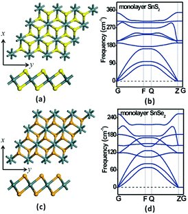 | ||
| Fig. 1 Top and side views of the optimized monolayer (a) SnS2 and (c) SnSe2. (b) and (d) are the phonon spectra of the optimized SnS2 and SnSe2 monolayers. | ||
The analysis of phonon dispersion can provide a reliable test for the quality of structure optimization and the dynamical stability of structures. To check the dynamical stability of the SnS2 and SnSe2 monolayers as well as whether their structures are well optimized, the phonon spectra were calculated based on the same DFT level and shown in Fig. 1b and d. It is noted that there is no imaginary frequency in both the SnS2 and SnSe2 monolayer systems, which confirms their kinetical stability and well optimized structures. In details, the acoustic and optic vibration frequencies of monolayer SnS2 are 0–150 cm−1 and 190–350 cm−1 (Fig. 1b), while those of the monolayer SnS2 are 0–110 cm−1 and 120–250 cm−1 (Fig. 1d), respectively. Due to the lighter mass of S atom compared to Se atom, the Debye frequency of SnS2 is ∼100 cm−1 bigger than that of monolayer SnSe2. In order to compare the band gaps of bulk phase and monolayers for SnS2 and SnSe2, the electronic structures of SnS2 and SnSe2 were calculated at HSE06 level (shown in Fig. S1†), and the calculated band gaps of bulk phase and monolayers for SnS2 and SnSe2 are in good accordance with the experimental results,56,57 showing our calculated results are reliable.
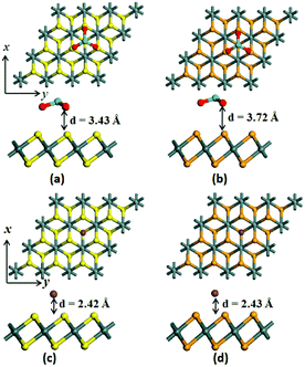
To explore the surface modification effects on the monolayer SnS2 and SnSe2, an electron-withdrawing dopant (MoO3), and an electron-donating dopant (alkali metal atom, K) were chosen in this paper, as shown in Fig. 2. The equilibrium closest vertical distances between MoO3/K and the monolayer SnS2/SnSe2 are ∼3.43/2.42 and ∼3.72/2.43 Å, respectively. The equilibrium distances between the K atom and the monolayers are much smaller than that between the MoO3 molecule and the monolayers, indicating a much stronger interactions between K atom and the monolayers. This is confirmed by the adsorption energies, where the adsorption energies of K modified monolayers are about two times as those of MoO3 modified monolayers (Table 1). The stronger interaction between the K atom and monolayers finally leads to about two times charge transfer amount compared to that of MoO3 molecule, as shown in Table 1. Specifically, there are 0.37 and 0.4 |e| charges transferred from the SnS2/SnSe2 monolayers to the MoO3 molecule, respectively. As for K atom adsorption, 0.79 and 0.74 |e| charges are injected from K atom into the monolayer SnS2 and SnSe2, respectively. The large electron withdrawing/donating ability of MoO3 and K indicates that they are efficient p- and n-type dopants.
| Geometries | ΔE/eV | qads/e | qSnX2/e | ΔΦ/eV |
|---|---|---|---|---|
| a ΔΦ is defined as ΔΦ = Φdopant/SnX2 − ΦSnX2, where Φdopant/SnX2 and ΦSnX2 are the work functions of the surface modified system and the intrinsic monolayer SnX2 (X = S, Se), respectively. | ||||
| MoO3-modified SnS2 | −1.32 | −0.37 | 0.37 | 0.73 |
| MoO3-modified SnSe2 | −1.44 | −0.40 | 0.40 | 0.30 |
| K-modified SnS2 | −3.43 | 0.79 | −0.79 | −1.48 |
| K-modified SnSe2 | −3.22 | 0.74 | −0.74 | −1.33 |
The change of carrier concentration will be reflected by the variations of work functions in semiconductors. Therefore, electrostatic potential calculations were further performed to probe the change of work functions (ΔΦ) for monolayer SnS2 and SnSe2 before and after MoO3 and K doping. As shown in Table 1, the adsorption of MoO3 molecule on the surface of monolayer SnS2 and SnSe2 yields an obvious increase of work function by 0.73 and 0.6 eV, respectively. This result can be attributed to the injection of holes from the MoO3 molecule into the monolayers, which downshifts the Fermi level of the system. In contrast, a large decrease of work function takes place after the adsorption of K on the monolayer SnS2 and SnSe2 due to the upshift of Fermi level into the conduction band region. The above analysis indicates that monolayer SnS2 and SnSe2 may be tuned into p-type conductivity by doping with the electron-drawing MoO3 molecule, while the adsorption of K atoms would enhance the n-type conductivity of monolayer SnS2 and SnSe2.
As mentioned above, both MoO3 and K can strongly interact with the monolayer SnS2 and SnSe2 and a considerable charge transfer between the dopants and monolayers occurs. Such a modification will for sure change the electronic and optical properties of monolayer SnS2 and SnSe2. To illustrate how surface doping changes the electronic properties, the band structures of monolayer SnS2 and SnSe2 before and after surface modifications under the same computational conditions were calculated, as shown in Fig. 3.
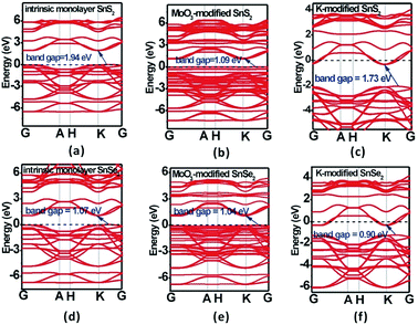 | ||
| Fig. 3 Band structures of (a) and (d) intrinsic, (b) and (e) MoO3-modified, and (c) and (f) K-modified SnS2 and SnSe2 monolayers at the GGA-PBE level. | ||
It can be noted that both monolayer SnS2 and SnSe2 are indirect-band-gap semiconductors with 1.94 and 1.07 eV bandgaps at the GGA/PBE level (Fig. 3a and d), respectively, but 3.03 and 2.01 eV at the HSE06 level (Fig. S1†), which are in good accordance with experimental and computational results.56,57 Although the PBE functional usually underestimates bandgaps to some degree, it does not affect our analysis of bandgap variations and Fermi level shifting. Due to the strong non-covalent interaction and considerable charge transfer between the surface dopants (MoO3 and K) and the monolayer SnS2 and SnSe2, the MoO3 and K modified systems exhibit decreased bandgaps, as shown in Fig. 3. Interestingly, a new flat energy level is generated in the original bandgaps of MoO3 modified systems, leading to reduced bandgaps of 1.09 and 1.03 eV, respectively. Moreover, the Fermi level moves to the top of valance band in MoO3 modified systems, confirming a p-type semiconductor characteristic. In contrast, the Fermi level moves into the conduction band after the adsorption of K on the monolayer SnS2 and SnSe2, manifesting the great enhancement of n-type conductivity for monolayer SnS2 and SnSe2. Therefore, it is evident that MoO3 is a hole dopant and it can be used to achieve p-type doping in monolayer SnS2 and SnSe2, while K as an electron dopant can enhance the n-type conductivity of monolayer SnS2 and SnSe2. The partial density of states (PDOS) of for intrinsic and surface-modified monolayer SnS2 and SnSe2 was also computed (Fig. 4), which validates the results from band structure calculations.
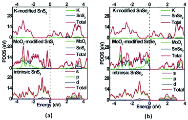 | ||
| Fig. 4 The partial density of states (PDOS) for intrinsic and surface-modified (a) SnS2 and (b) SnSe2 monolayers at the GGA-PBE level. | ||
To have a deeper insight into the electronic properties of the surface modified monolayer SnS2 and SnSe2 systems and visualize the charge transfer between the surface dopants (MoO3 and K) and the monolayers, we further computed the electron density difference (Δρ), which is defined as Δρ = ρmolecule/substrate – ρmolecule – ρsubstrate, in which ρmolecule/substrate, ρmolecule and ρsubstrate denote the electron density of the molecule modified systems, the isolated surface dopants and the monolayers, respectively. The electron density difference illustrates how the electron density changes during the adsorption process. As shown in Fig. 5, there is a significant variation of the electron density at the interfaces due to the adsorption of MoO3 and K on the SnS2/SnSe2 monolayers, where the red and blue colors denote the electron loss and enrichment, respectively. A strong electron accumulation is observed around the MoO3 molecule, while regions of depletion appear on the surface of the SnS2/SnSe2 monolayers. Opposite phenomenon can be found for the K modified systems. These phenomena directly illustrate that the MoO3 molecule draws electrons from the SnS2/SnSe2 monolayers while the K atoms donate electrons to the SnS2/SnSe2 monolayers. The redistribution of electrons between electron-drawing dopant (MoO3) is responsible for the formation of a dipole pointing from the substrate to the MoO3 molecule, while the redistribution of electrons between electron-donating dopant (K) is responsible for the formation of a dipole pointing from the K atom to the substrate. The above results stemmed from Fig. 5 are supported by the Mulliken population analysis in Table 1. Together with the band structures, it proves the adsorption of MoO3 and K can dramatically change the electronic properties of SnS2 and SnSe2 monolayers.
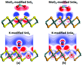 | ||
| Fig. 5 Electron density difference of MoO3 and K modified monolayers (a) SnS2 and (b) SnSe2. Red and blue colors represent electron accumulation and depletion, respectively. | ||
Since the band structures of the monolayer SnS2/SnSe2 can be effectively tuned by the adsorption of MoO3 and K, their optical properties, which are directly related to the band structures, are expected to be modified by surface doping as well. Thus, we calculated the imaginary parts of the dielectric functions (ε2), which is an effective parameter to measure the optical absorption ability of materials.61,62 From Fig. 6, it can be noted that an appreciable new absorption peak appears at ∼650/∼600 nm after MoO3 adsorbed on the monolayer SnS2/SnSe2. For K modified monolayer SnS2/SnSe2, the new adsorption peaks are located at ∼480 and 680 nm, respectively. The appearance of new absorption peaks is a direct result of the reduced bandgaps with surface doping, which effectively enhances the absorption ability of the monolayer SnS2/SnSe2 in visible region. Interestingly, the adsorption of MoO3 on monolayer SnS2/SnSe2 not only widens the adsorption region, but also enhances the adsorption intensity, which is particularly useful for light harvesting. The broadened absorption range reveals that the surface doping paves an efficient way to widen the applications of monolayer SnS2/SnSe2 in water splitting and environmental pollutants degradation fields.
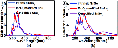 | ||
| Fig. 6 Computed imaginary dielectric functions versus the wavelength for the pristine (blue lines), MoO3 (red lines) and K (purple lines) functionalized (a) SnS2 and (b) SnSe2 monolayers. | ||
Conclusions
In conclusion, we systematically investigated the electronic and optical properties of monolayer SnS2/SnSe2 before and after surface modification with electron-drawing (MoO3) and electron-donating (K) dopants by means of first principles calculations. It was found that both MoO3 and K have an obvious effect on the electronic and optical properties of monolayer SnS2/SnSe2. The adsorption of MoO3 withdraws the electrons from the monolayer SnS2 and SnSe2 and introduces a new flat impurity band in the original band gap of the monolayers, as a result, the Fermi level correspondingly moves to the top of valance band, which leads to a p-type semiconductor characteristic. In contrast, the adsorption of K atom injects electrons into the monolayer SnS2/SnSe2 and the Fermi level moves into the conduction band, which enhances the n-type conductivity of the monolayer SnS2/SnSe2. The band gaps of both MoO3 and K doped SnS2 and SnSe2monolayers are reduced due to the significant charge transfer between surface dopants (MoO3 and K) and monolayers. Moreover, appreciable new absorption peaks appear around ∼650/480 and ∼600/680 nm after MoO3/K adsorption on the monolayer of SnS2 and SnSe2, respectively, which paves a way to design new efficient sunlight absorber materials. Our results suggest that the surface modification is an efficient way to tune the electronic and optical properties of the monolayer SnS2/SnSe2, which would broaden the applications of the monolayer SnS2/SnSe2 in water splitting and environmental pollutants degradation fields.Conflicts of interest
There are no conflicts to declare.Acknowledgements
This work was supported by the National Natural Science Foundation of China (No. 21703087, 21406020, 21373103) and the Natural Science Foundation of Jiangsu Province (No. BK20140257). We acknowledge the computing resources and technical support from National Super Computing Center in Shenzhen (Shenzhen Cloud Computing Center).Notes and references
- A. Fujishima and K. Honda, Nature, 1972, 238, 37–38 CrossRef CAS PubMed.
- M. A. Fox and M. T. Dulay, Chem. Rev., 1993, 93, 341–357 CrossRef CAS.
- M. R. Hoffmann, S. T. Martin, W. Choi and D. W. Bahnemann, Chem. Rev., 1995, 95, 69–96 CrossRef CAS.
- H. Tang, F. Levy, H. Berger and P. E. Schmid, Phys. Rev. B, 1995, 52, 7771–7774 CrossRef CAS.
- M. Gräatzel, Nature, 2001, 414, 338–344 CrossRef PubMed.
- D. E. Carlson and C. R. Wronski, Appl. Phys. Lett., 1976, 28, 671 CrossRef CAS.
- J. Z. Ou, W. Y. Ge, B. Carey, T. Daeneke, A. Rotbart, W. Shan, Y. C. Wang, Z. Q. Fu, A. F. Chrimes, W. Wiodarski, S. P. Russo, Y. X. Li and K. Kalantar-zadeh, ACS Nano, 2015, 9, 10313–10323 CrossRef CAS PubMed.
- M. Chen, Z. K. Li, W. M. C. W. Li, W. J. Li, K. W. Li, G. D. Gu, Y. Feng, G. H. Zhong, L. Wei and C. L. Yang, Nanotechnology, 2018, 29, 455501 CrossRef PubMed.
- P. Chen, Y. Su, H. Liu and Y. Wang, ACS Appl. Mater. Interfaces, 2013, 5, 12073–12082 CrossRef CAS PubMed.
- Z. X. Wei, L. Wang, M. Zhuo, W. Ni, H. X. Wang and J. M. Ma, J. Mater. Chem. A, 2018, 6, 12185–12214 RSC.
- Y. F. Sun, H. Cheng, S. Gao, Z. H. Sun, Q. H. Liu, Q. Liu, F. C. Lei, T. Yao, J. F. He, S. Q. Wei and Y. Xie, Angew. Chem., Int. Ed., 2012, 51, 8727–8731 CrossRef CAS PubMed.
- X. X. Zhu, X. K. Luo, H. K. Yuan, H. Chen and C. L. Tian, RSC Adv., 2018, 8, 3304–3311 RSC.
- L. A. Burton, T. J. Whittles, D. Hesp, W. M. Linhart, J. M. Skelton, B. Hou, R. F. Webster, G. O'Dowd, C. Reece, D. Cherns, D. J. Fermin, T. D. Veal, V. R. Dhanak and A. Walsh, J. Mater. Chem. A, 2016, 4, 1312–1318 RSC.
- Z. Z. Cheng, F. M. Wang, T. A. Shifa, C. Jiang, Q. L. Liu and J. He, Small, 2017, 13, 1702163 CrossRef PubMed.
- H. L. Zhuang and R. G. Hennig, Phys. Rev. B: Condens. Matter Mater. Phys., 2013, 88, 115314 CrossRef.
- J. Yu, C. Y. Xu, F. X. Ma, S. P. Hu, Y. W. Zhang and L. Zhen, ACS Appl. Mater. Interfaces, 2014, 6, 22370–22377 CrossRef CAS PubMed.
- W. L. Fu, J. M. Wang, S. Y. Zhou, R. J. Li and T. Y. Peng, ACS Appl. Nano Mater., 2018, 1, 2923–2933 CrossRef CAS.
- P. Wahnon, J. C. Conesa, P. Palacios, R. Lucena, I. Aguilera, Y. Seminovski and F. Fresno, Phys. Chem. Chem. Phys., 2011, 13, 20401–20407 RSC.
- H. L. Zhuang and R. G. Hennig, Phys. Rev. B, 2013, 88, 115314 CrossRef.
- G. Z. Qiu, H. M. Zhang, Y. M. Liu and C. Y. Xia, Phys. B, 2018, 547, 1–5 CrossRef CAS.
- L. Hu, X. F. Song, S. L. Zhang, H. B. Zeng, X. J. Zhang, R. Marks and D. Shan, J. Catal., 2018, 366, 8–15 CrossRef CAS.
- G. P. Zhang, D. Y. Chen, N. J. Li, Q. F. Xu, H. Li, J. H. He and J. M. Lu, J. Colloid Interface Sci., 2018, 514, 306–315 CrossRef CAS PubMed.
- X. X. Zhu, X. K. Luo, H. K. Yuan, H. Chen and C. L. Tian, RSC Adv., 2018, 8, 3304–3311 RSC.
- J. H. Liu, G. F. Huang, W. Q. Huang, H. Miao and B. X. Zhou, Mater. Lett., 2015, 161, 480–483 CrossRef CAS.
- C. X. Xia, Y. T. Peng, H. Zhang, T. X. Wang, S. Y. Wei and Y. Jia, Phys. Chem. Chem. Phys., 2014, 16, 19674–19680 RSC.
- Z. C. Wu, Y. J. Xue, Y. L. Zhang, J. J. Li and T. Chen, RSC Adv., 2015, 5, 24640–24648 RSC.
- H. Xiang, B. Xu, Y. D. Xia, J. Yin and Z. G. Liu, Sci. Rep., 2016, 6, 39218 CrossRef CAS PubMed.
- E. P. Mukhokosi, S. B. Krupanidhi and K. K. Nanda, Sci. Rep., 2017, 7, 15215 CrossRef PubMed.
- Y. Huang, K. Xu, Z. X. Wang, T. A. Shifa, Q. S. Wang, F. Wang, C. Jiang and J. He, Nanoscale, 2015, 7, 17375–17380 RSC.
- C. Ling and F. Mizuno, Phys. Chem. Chem. Phys., 2014, 16, 10419–10424 RSC.
- A. Samad, M. Noor-A-Alam and Y. H. Shin, J. Mater. Chem. A, 2016, 4, 14316–14323 RSC.
- X. An, C. Y. Jimmy and J. Tang, J. Mater. Chem. A, 2014, 2, 1000–1005 RSC.
- Y. M. Liu, F. Wang, D. C. Kong, B. Hu, C. X. Xia and J. X. Su, Phys. Lett. A, 2017, 381, 1732–1737 CrossRef CAS.
- J. Ristein, Science, 2006, 313, 1057–1058 CrossRef CAS PubMed.
- W. Chen, D. C. Qi, X. Y. Gao and A. T. S. Wee, Prog. Surf. Sci., 2009, 84, 279–321 CrossRef CAS.
- Z. Y. Yin, M. Tordjman, Y. Lee, A. Vardi, R. Kalish and J. A. Del Alamo, Sci. Adv., 2018, 4, 0480 Search PubMed.
- F. F. Xia, Z. B. Shao, Y. Y. He, R. B. Wang, X. F. Wu, T. H. Jiang, S. Duhm, J. W. Zhao, S. T. Lee and J. S. Jie, ACS Nano, 2016, 10, 10283–10293 CrossRef CAS.
- T. Xiong, W. L. Cen, Y. X. Zhang and F. Dong, ACS Catal., 2016, 6, 2462–2472 CrossRef CAS.
- W. J. Wang, P. Xu, M. Chen, G. M. Zeng, C. Zhang, C. Y. Zhou, Y. Yang, D. L. Huang, C. Lai, M. Cheng, L. Hu, W. P Xiong, H. Guo and M. Zhou, ACS Sustainable Chem. Eng., 2018, 6, 15503–15515 CrossRef CAS.
- F. L. Yang, F. F. Xia, J. Hu, C. Z. Zheng, J. H. Sun and H. B. Yi, RSC Adv., 2018, 8, 1899–1904 RSC.
- R. M. Zhao, T. X. Wang, M. Y. Zhao, C. X. Xia, X. Zhao, Y. P. An and X. Q. Dai, Phys. Chem. Chem. Phys., 2017, 19, 10470–10480 RSC.
- Y. C. Huang, D. M. Zhou, X. Chen, H. Liu, C. Wang and S. F. Wang, ChemPhysChem, 2016, 17, 375–379 CrossRef CAS.
- P. Hohenberg and W. Kohn, Phys. Rev. B, 1964, 136, B864–B871 CrossRef.
- W. Kohn and L. Sham, Phys. Rev., 1965, 140, A1133–A1138 CrossRef.
- S. J. Clark, M. D. Segall, C. J. Pickard, P. J. Hasnip, M. I. J. Probert, K. Refson and M. C. Payne, Z. Kristallogr., 2005, 220, 567–570 CAS.
- P. H. T. Philipsen, G. te Velde and E. J. Baerends, Chem. Phys. Lett., 1994, 226, 583–588 CrossRef CAS.
- A. Zupan, K. Burke, M. Ernzerhof and J. P. Perdew, J. Chem. Phys., 1997, 106, 10184–10193 CrossRef CAS.
- B. Hammer, K. W. Jacobsen and J. K. Norskov, Phys. Rev. Lett., 1993, 70, 3971–3974 CrossRef CAS PubMed.
- B. Hammer and M. Scheffler, Phys. Rev. Lett., 1995, 74, 3487–3490 CrossRef CAS PubMed.
- J. P. Perdew and Y. Wang, Phys. Rev. B, 1992, 45, 13244–13249 CrossRef.
- J. P. Perdew, K. Burke and M. Ernzerhof, Phys. Rev. Lett., 1996, 77, 3865–3868 CrossRef CAS PubMed.
- J. P. Perdew, A. Ruzsinszky, G. I. Csonka, O. A. Vydrov, G. E. Scuseria, L. A. Constantin, X. Zhou and K. Burke, Phys. Rev. Lett., 2008, 100, 136406 CrossRef PubMed.
- S. Grimme, J. Comput. Chem., 2006, 27, 1787–1799 CrossRef CAS PubMed.
- D. Vanderbilt, Phys. Rev. B, 1990, 41, 7892–7895 CrossRef.
- H. J. Monkhorst and J. D. Pack, Phys. Rev. B, 1976, 13, 5188–5192 CrossRef.
- J. Robertson, J. Phys. C: Solid State Phys., 1979, 12, 4753–4766 CrossRef CAS.
- A. Ibarz, E. Ruiz and S. Alvarez, Chem. Mater., 1998, 10, 3422–3428 CrossRef CAS.
- L. A. Burton, D. Colombara, R. D. Abellon, F. C. Grozema, L. M. Peter, T. J. Savenije, G. Dennler and A. Walsh, Chem. Mater., 2013, 25, 4908–4916 CrossRef CAS.
- Y. C. Huang, C. Y. Ling, H. Liu, S. Y. Wang and B. Y. Geng, J. Phys. Chem. C, 2014, 118, 9251–9260 CrossRef CAS.
- C. X. Xia, Y. T. Peng, H. Zhang, T. X. Wang, S. Y. Wei and Y. Jia, Phys. Chem. Chem. Phys., 2014, 16, 19674–19680 RSC.
- M. Gajdos, K. Hummer, G. Kresse, J. Furthmuller and F. Bechstedt, Phys. Rev. B, 2006, 73, 045112 CrossRef.
- C. Ambrosch-Draxl and J. O. Sofo, Comput. Phys. Commun., 2006, 175, 1–14 CrossRef CAS.
Footnote |
| † Electronic supplementary information (ESI) available. See DOI: 10.1039/c8ra08834a |
| This journal is © The Royal Society of Chemistry 2018 |

