DOI:
10.1039/C8RA08563C
(Paper)
RSC Adv., 2018,
8, 40298-40307
Study of the effect of DIO additive on charge extraction and recombination in organic–inorganic hybrid MAPbI3−xClx perovskite solar cell
Received
16th October 2018
, Accepted 19th November 2018
First published on 4th December 2018
Abstract
In this article, we fabricated a plane structure perovskite solar cell of ITO/PEDOT:PSS/MAPbI3−xClx/PCBM/Al. With 1% of 1,8-diiodooctane (DIO) additive in the perovskite, the solar cell's efficiency greatly increased from 10.39% to 13.57%. On the one hand, the DIO additive is advantageous to enhance the thin-film degree of crystallinity, and it can enhance the perovskite thin film's electrical polarization characteristic, leading to an increase in the built-in electric field, and promote charge extraction and separation and transport processes. On the other hand, the DIO additive can also enhance the charge extraction speed in the perovskite solar cell photoelectric conversion process, and further increase the power conversion efficiency (PCE) of the perovskite solar cell. In addition, in the perovskite solar cell device there occurs the monomolecular recombination effect; the DIO additive introduced into the perovskite can effectively reduce the trap-induced monomolecular recombination effect, and enhance the solar cell's PCE.
1. Introduction
In recent years, many authors1–4 have reported that in an acceptor material, adding a third component material (additive) could effectively control the active layer's morphology. Using this method may lead to great economies in device post-processing, simplify device preparation technology, and allow realization of the most optimized efficiency. Additive selection is very closely related to materials systems; if the compatibility of donor and acceptor materials is not good in the active layer, the degree of phase separation will greatly increase after forming the thin film. Therefore, the selected additive material needs to have good compatibility with the donor and acceptor materials, and the boiling point of the additive must be higher than that of the main solvent material. When adding the additive to the donor and acceptor materials, if the donor and acceptor materials were a uniform mixture, but the degree of phase separation was small, they still could not form an interpenetrating network structure. Hence, controlling the degree of phase separation of donor and acceptor materials is very important in the active layer. It is useful for the donor material's transport properties, which can promote power conversion efficiency (PCE) enrichment. In experiments, the use of an additive is a good and simple method to control the degree of phase separation. For example, Su et al.5 added a small amount of 1,4-diiodobutane to PBTTPD![[thin space (1/6-em)]](https://www.rsc.org/images/entities/char_2009.gif) :PC71BM, which effectively increased PBTTPD crystal characteristic, reduced PC71BM aggregation, promoted the donor–acceptor cross-penetrating network structure, and enhanced PCE to 7.3%. Peet et al.6 added alkyldimercaptan to PCPDTBT:PCBM solution, which increased the molecular chain interaction and enhanced the hole mobility, leading to the PCE of perovskite solar cell reaching 5.5%. In the perovskite field, Alex et al.7,8 added a certain amount of 1,8-diiodooctane (DIO) to a perovskite polymeric precursor solution to improve the perovskite's morphology. The addition of DIO could increase the perovskite's crystalline property, and enhance the thin film's rate of coverage, improving the PCE of the perovskite solar cell from 9.0% to 11.8%. Yang et al. added DIO to control the morphology and structure of CH3NH3PbI3 perovskite thin films, and increased the PCE of perovskite solar cells from 4.5 to 9.0%.9
:PC71BM, which effectively increased PBTTPD crystal characteristic, reduced PC71BM aggregation, promoted the donor–acceptor cross-penetrating network structure, and enhanced PCE to 7.3%. Peet et al.6 added alkyldimercaptan to PCPDTBT:PCBM solution, which increased the molecular chain interaction and enhanced the hole mobility, leading to the PCE of perovskite solar cell reaching 5.5%. In the perovskite field, Alex et al.7,8 added a certain amount of 1,8-diiodooctane (DIO) to a perovskite polymeric precursor solution to improve the perovskite's morphology. The addition of DIO could increase the perovskite's crystalline property, and enhance the thin film's rate of coverage, improving the PCE of the perovskite solar cell from 9.0% to 11.8%. Yang et al. added DIO to control the morphology and structure of CH3NH3PbI3 perovskite thin films, and increased the PCE of perovskite solar cells from 4.5 to 9.0%.9
It is well known that charge recombination is an important energy loss in the light current formation process. In a polymer/perovskite solar cell, according to the electron–hole pair property differences, charge recombination can occur, including geminate recombination and nongeminate recombination.10 Geminate recombination is where the active layer absorbs the same photon to generate an electron–hole pair, and the electron–hole pair is held together by the Coulomb force before separating the free carrier. In nongeminate recombination, a different photon is absorbed to generate an electron–hole pair, and the electron–hole pair will recombine by the Coulomb force in the transport process. Usually, in an experiment, we can distinguish the geminate recombination from nongeminate recombination by observing the recombination time and the dependency relation of recombination process and carrier concentration. Specifically, the geminate recombination process happens very quickly, on a timescale at the nanosecond level, and it has no relation to the carrier concentration. But nongeminate recombination is related to carrier concentration, and the process happens on the microsecond and millisecond timescale after initiation.
In addition, according to the internal carrier contributing to the recombination effect, charge combination can also be divided into monomolecular recombination and bimolecular recombination.11 The probability of bimolecular recombination contacts is related to two kinds of carrier densities of electrons and holes: R ∝ ne, nh, (where R is the probability of recombination and ne, nh are the density of electrons and holes, respectively). However, the probability of monomolecular recombination is only related to one kind of carrier density, that of either electrons or holes: R ∝ ne or R ∝ nh. In general, if a device has no trap state, photoexcitation generates electrons and holes, and the recombination process belongs to bimolecular recombination. But in a device having trap and defect states, the device has a mass of trap states (holes or electrons), electrons and holes can recombine with these defect charges, the probability is related to one kind of carrier density, and this trap-assisted recombination process belongs to monomolecular recombination. At present, many methods have been used to study the recombination process in polymer/perovskite solar cells; for example, time-of-flight,12 steady-state current–voltage,13 impedance spectroscopy,14 photoinduced charge extraction by linearly increasing voltage, photo-CELIV,15 transient absorption and transient photoconductivity,16 etc. Cowan et al.17 used the impedance spectroscopy and steady-state current–voltage methods to study the charge recombination mechanism in the PCDTBT and P3HT system. They found that bimolecular recombination was the main recombination process when the device was in the open circuit voltage condition, and the bimolecular recombination process was a voltage-dependent and charge concentration process. Koster et al.18 utilized the steady-state differential current to study the bimolecular recombination process of a P3HT:PCBM solar cell under different annealing conditions. Mozer et al.15 reported a detailed study of the charge mobility and charge recombination dynamics process under different delay time and light intensity and applied bias by photo-induced charge extraction by linearly increasing voltage.
Given all this, an additive not only can control the degree of phase separation of donor and acceptor materials but also can effectively suppress charge recombination. In this article, we fabricated an ITO/PEDOT:PSS/MAPbI3−xClx/PCBM/Al structure solar cell, utilized the additive of DIO to improve the perovskite's thin-film morphology and to increase the perovskite solar cell's PCE. We studied the perovskite thin film's surface morphology and electrical polarization properties by the light absorption characteristic, X-ray diffraction (XRD), scanning electron microscopy (SEM), atom force microscopy (AFM), and capacitance–voltage relationship, utilized the transient photocurrent method to study how the additive affects the charge transport and collection process, and utilized the different light intensity current–voltage curve characteristic to analyze the influence of the additive on the charge recombination mechanism.
2 Experimental section
2.1 Perovskite material preparation
CH3NH3I, PbI2 and PbCl2 were purchased from the Materials Co. in Canada and Alfa Aesar Co. in China. PbI2, PbCl2 and CH3NH3I3 (2 M:1 M:1 M) were dissolved in N,N-dimethylformamide (DMF; Aldrich Co.) as the precursor solutions.19 All of the precursor solutions were stirred at 80 °C for 12 h, which when the mass concentration was 30 wt% gave polymeric precursor solution. The hole transport layer used PEDOT:PSS (AI4083, Sigma-Aldrich), purchased from Bayer Co., Germany. The electron transport layer used phenyl-C60-butyric acid methyl ester (PC60BM) material, purchased from Banhe Technology Co. The PC60BM concentration was 20 mg mL−1, dissolved in chlorobenzene (Aldrich Co.), and stirred at 80 °C for 6 h. Electrodes for anode and cathode were ITO and aluminum (Al) electrodes, respectively. The whole device structure is ITO/PEDOT:PSS/perovskite/PCBM/Al.
2.2 Perovskite solar cell device preparation
Firstly, laser-patterned, ITO-coated glass substrates were cleaned by ultrasonic oscillation in an alkaline, aqueous washing solution for 15 min. Afterwards, they were rinsed successively with deionized water, ethanol and acetone, then placed into an O3 condition using ultraviolet treatment for 30 min. PEDOT:PSS was deposited by spin-coating at 5000 rpm for 30 s to give a thickness of 40 nm. All thickness measurements of thin films used surface step profilers (Brooker Co., Germany). Afterwards, the prepared perovskite (MAPbI3−xClx) was spin-coated on the PEDOT:PSS thin film at 1000 rpm for 10 s, followed by 4000 rpm for 35 s. The thin film was immediately annealed at 70 °C for 80 min. After cooling down, PC60BM (20 mg mL−1 in chlorobenzene) was spin-coated on top of the perovskite film at 2000 rpm for 45 s, followed by spin-coating an interface-modifying layer of PEIE (0.1 wt%, in anhydrous 2-propanol) at 5000 rpm for 60 s. Finally, 80 nm thick Al layers were thermally deposited as the top electrodes under a vacuum of 4 × 10⁻⁴ Pa to fabricate perovskite solar cells with an area of 9 mm2. All devices were encapsulated by epoxy resin in a glove box for experimental measurements. The device structure is shown in Fig. 1. The DIO (Aldrich) concentrations were 0.2, 0.6, 1.0 and 1.5 wt%, added into the perovskite polymeric material as the precursor solution, and heated with stirring for 12 h at 80 °C.
 |
| | Fig. 1 Perovskite solar cell structure and DIO molecular structure. | |
2.3 Device characteristic measurement
Photovoltaic measurements were conducted using an AM 1.5 solar simulator equipped with a 450 W xenon lamp (Newport). The power output was adjusted to match AM 1.5 global sunlight (100 mW cm−2 by using a reference Si solar cell). Current density–voltage (J–V) curves were obtained by applying an external bias to the cell and measuring the generated photocurrent with a Keithley model 2400 digital source meter. The voltage step and delay time of photocurrent were 10 mV and 100 ms, respectively. A similar data acquisition system was used to determine the monochromatic incident photon to electric current conversion efficiency. Under full computer control, light from a 300 W xenon lamp was focused through a Gemini-180 double monochromator onto the photovoltaic cell to be tested. The monochromator was incremented through the visible spectrum to generate IPCE(λ), defined by IPCE(λ) = 12400 (Jsc/λφ), where λ is the wavelength, Jsc is the short-circuit photocurrent density (mA cm−2), and φ is the incident radiative flux (mW cm−2). Photovoltaic performance was measured by using a metal mask with an aperture area of 10 mm2. The measurements were performed under bias light. The cross section of the device was measured by using a Zeiss Jemini FEG-SEM instrument at 5 kV with magnification of 250k.
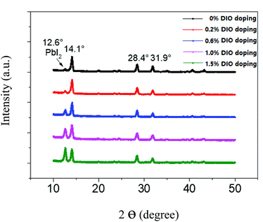
Fig. 2 shows the XRD patterns for the different DIO doping concentrations of 0.2, 0.6, 1.0 and 1.5 wt%. From the XRD results, we found that the pure perovskite shows several main peaks, the corresponding diffraction angles being 14.1°, 28.4°, 31.9°, respectively. It is evident that the materials fabricated from perovskite solutions crystallize in a tetragonal crystal structure. XRD reflections confirm the MAPbI3−xClx perovskite structure with lattice parameters a = b = 8.8724 Å and c = 12.5475 Å for the control sample and a = b = 8.8650 Å and c = 12.5370 Å for the sample with 1% DIO additive. In addition, in the XRD pattern there also appears a small peak at 12.6°, attributed to PbI2. When we added the DIO to the perovskite, the DIO additive has no effect on the perovskite phase structure, and no new peak appears. The DIO addition, on the one hand, makes the grain size of perovskite become larger; on the other hand, it increases the PbI2 grain size, making its phase structure characteristic become more prominent.
 |
| | Fig. 2 XRD patterns for the pure and variously DIO-doped perovskite. | |
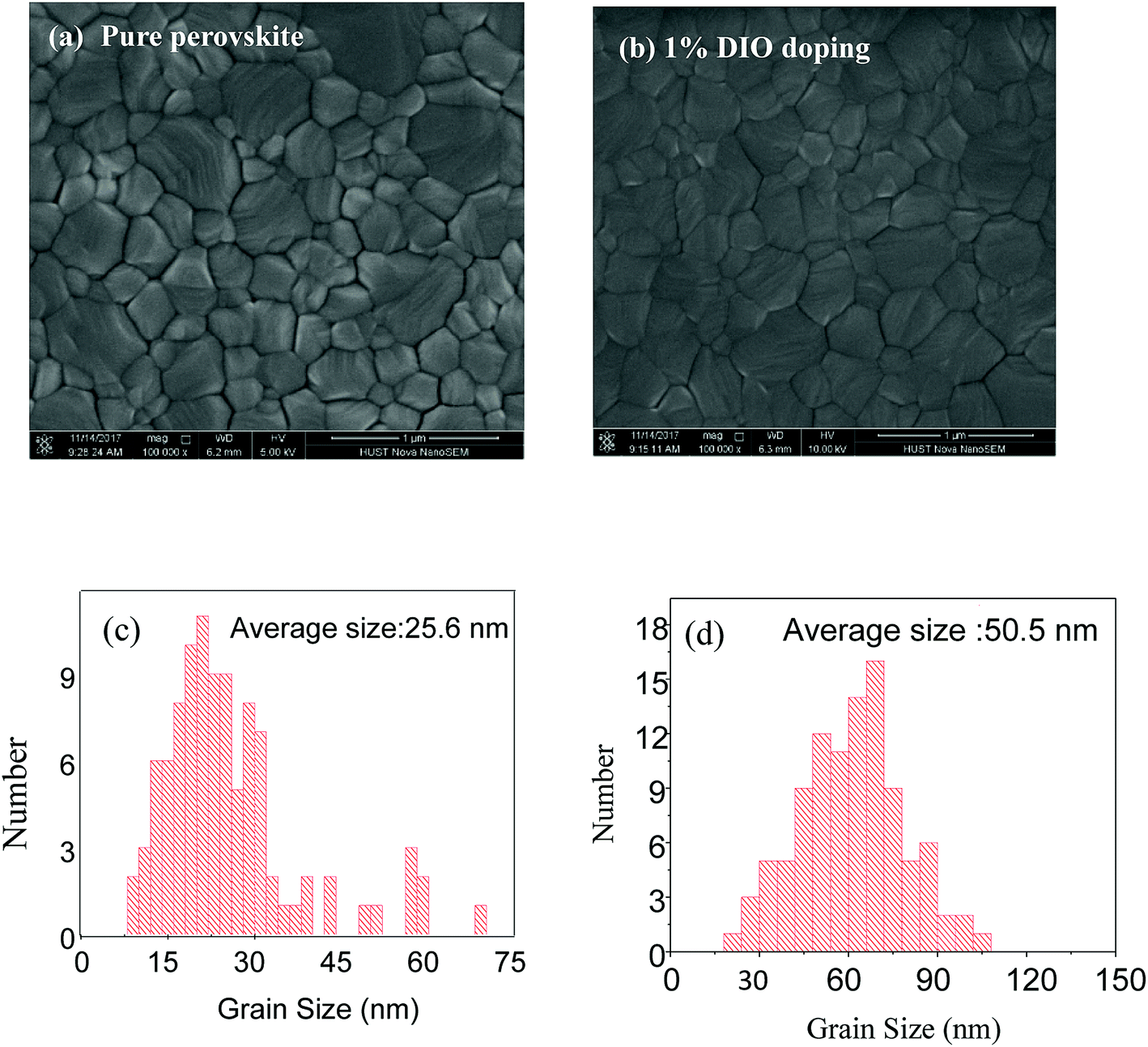
Fig. 3 shows SEM images of the pure and 1% DIO-doped perovskite thin films. We observed that both samples show full coverage on the substrate with the absence of pinholes. The perovskite grain size appears to be significantly enlarged by the addition of DIO, increasing from an average value of 25.6 to 50.5 nm for control and DIO-modified samples, respectively, and there is an increase the crystallinity of the perovskite thin film. We note that the SEM imaging is only sensitive to the surface of the film. We presumed that the grains are predominantly propagating throughout the thickness of the film, but cannot exclude the possible presence of smaller crystallites at the buried interface.
 |
| | Fig. 3 SEM images of the perovskite thin film: (a) pure perovskite; (b) 1% DIO doping. Grain size of (c) pure perovskite and (d) 1% DIO-doped perovskite. | |
3. Results and discussion
3.1 Additive's effect on device efficiency and perovskite thin-film morphology
Fig. 4 shows the current–voltage (I–V) characteristic curves of the perovskite solar cell with the DIO concentration changing from the 0.2 wt% to 1.5 wt%. We found the PCE of the perovskite solar cell first increased and then decreased. When the DIO additive concentration reached 1.0 wt%, the PCE also reached the maximum of 13.57%. From Table 1, we thought the reason for the PCE increase with the DIO additive concentration mainly came from the short-circuit current (Jsc) that increased quickly. Compared with the no DIO addition device, for which Jsc was only 17.30 mA cm−2, when DIO was added into the perovskite, Jsc increased quickly, the maximum Jsc being 19.76 mA cm−2 when the concentration of DIO was 1.0 wt%. This showed that the interior charge transport properties were enhanced after inserting the DIO additive into the perovskite. With continuing increase of DIO to 1.5 wt%, the PCE began to decrease; the greater DIO addition will affect the thin-film surface morphology, leading to a decrease in Jsc.
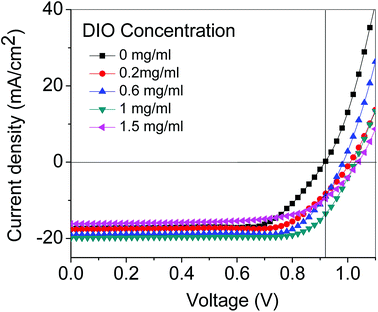 |
| | Fig. 4 Current–voltage characteristic curves of perovskite solar cell with various DIO concentrations. | |
Table 1 Perovskite solar cell's short-circuit current (Jsc), open-circuit voltage (Voc), fill factor (FF) and efficiency with the additive of DIO and with no additive
| Concentration of DIO additive (wt%) |
Open-circuit voltage (V) |
Short-circuit current (mA cm−2) |
Fill factor |
Efficiency (%) |
| 0 |
0.91 |
17.30 |
0.66 |
10.39 |
| 0.2 |
1.00 |
17.59 |
0.67 |
11.79 |
| 0.6 |
0.99 |
19.58 |
0.68 |
13.18 |
| 1 |
1.01 |
19.76 |
0.68 |
13.57 |
| 1.5 |
1.02 |
17.01 |
0.68 |
11.80 |
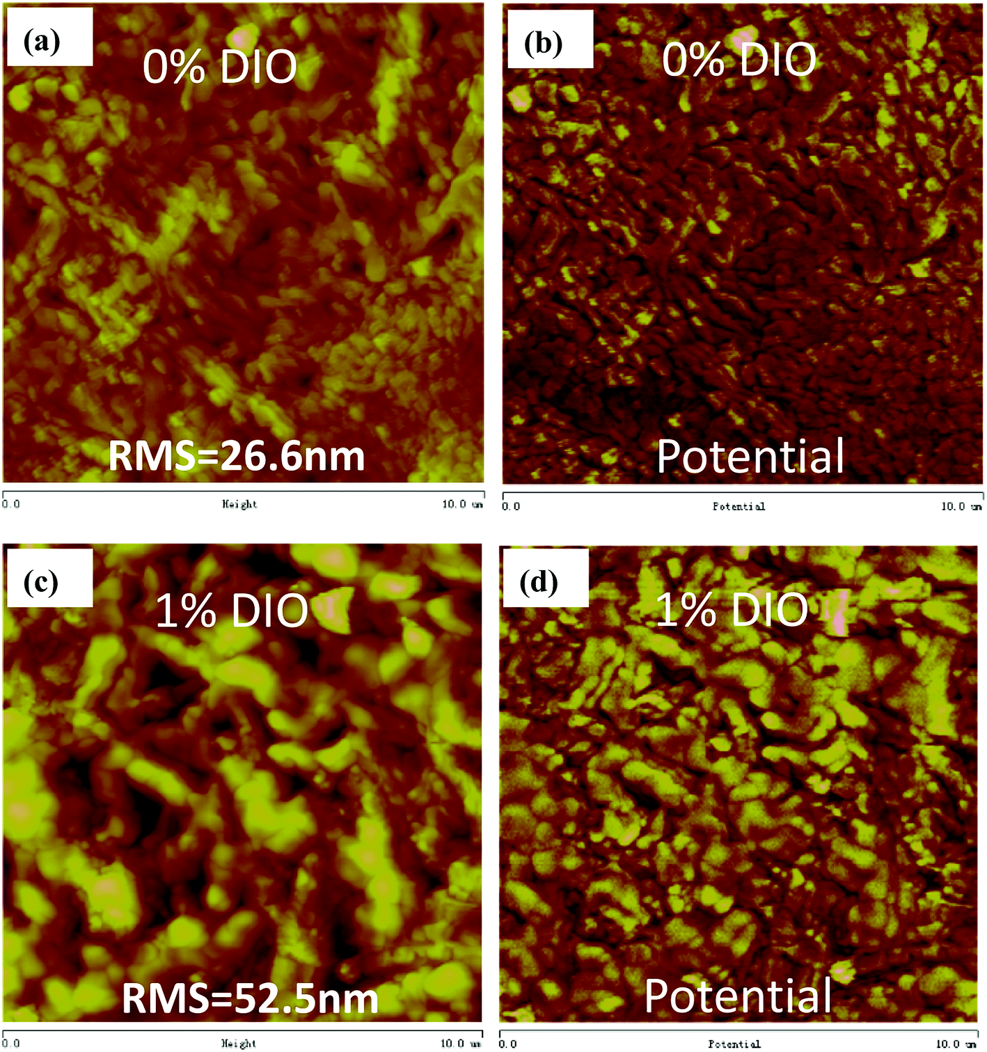
Fig. 5 shows the ultraviolet-visible absorption spectra of pure perovskite thin film and 1% DIO additive-doped perovskite thin film. From Fig. 5, we found that the absorption intensity of the perovskite thin film increased from 300 nm to 750 nm wavelength range when 1% DIO was added to the perovskite, leading to the number of photoinduction-generated carriers also increasing in the perovskite, resulting in an increase in the device's short-circuit current. Fig. 6 shows the surface morphology and surface potential distribution, measured by AFM. The AFM measurement results showed that the pure perovskite thin-film surface was uniform and smooth, its crystal size was small, and the roughness was RMS = 26.6 nm. With the addition of DIO, the perovskite thin film's aggregation extent was increased, the crystal size was obviously enlarged, and the aggregation extent was also increased, with RMS = 52.5 nm. These results showed that the DIO additive is useful to increase the perovskite's crystal properties, and increased the perovskite thin film's light absorption intensity, further confirming the results in Fig. 5. This also agreed with results reported in the literature.20 In addition, Fig. 6(b and d) shows that the perovskite surface potential decreased after 1% DIO addition. This indicated that the DIO additive could enhance the perovskite thin film's electric polarization properties, which is useful for charge separation and transport, and for enhancing the device's PCE.
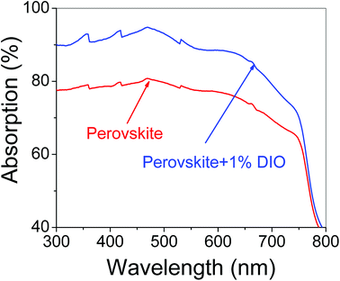 |
| | Fig. 5 Ultraviolet-visible absorption spectra of pure perovskite thin film and that with 1% DIO addition. | |
 |
| | Fig. 6 Pure perovskite thin film and 1% DIO additive-doped perovskite thin film surface morphology and potential distribution: (a and c) morphology; (b and d) potential distribution. The measurement range was 10 μm. | |
From Fig. 7 showing the device's capacitance–voltage (C−2–V) relation, we found the device's built-in potential increased. From Fig. 7 showing the 0% and 1% DIO-doped perovskite solar cell C−2–V curve in the illumination condition, we obtained that the built-in potential of the 0% DIO doping was Vbi = 0.63 V, and that of the 1% DIO doping was Vbi = 0.67 V. This indicated that the DIO could enhance the device's built-in electrical field, because the thickness was the same for the 0% and 1% DIO-doped perovskite thin films. The built-in potential enhancement meant the built-in electrical field was also increased, and the increased built-in electrical field has an important effect on charge transportation and extraction.
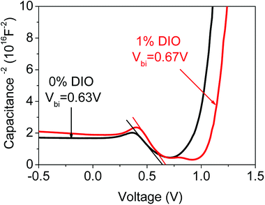 |
| | Fig. 7 C−2–V characteristic curves 0% DIO- and 1% DIO-doped perovskite thin films. | |
3.2 Additive's effect on the charge transportation and collection process
Now, we discuss the effect of the DIO additive on charge transportation and collection. In the perovskite solar cell, light can produce electron–hole pairs, and generate free charge carriers after electron–hole pair separation. When these free charges reach the electrode interface, they are extracted and collected by the electrode. Finally, an optical current is generated. Of these processes, charge transportation and charge extraction are the two most important ones, because the intrinsic trap state of perovskite material leads to the occurrence of photo-induced charge capture and decapture process, leading to a great of loss of photo-induce carriers. In addition, the imperfect electrode interface causes charge accumulation, which limits the charge extraction. In our experiment, we utilized the transient photoconductivity method to study the perovskite device's charge transportation and extraction process, used short pulses of light to excite the perovskite solar cell, and made the device interior produce a few carriers. These carriers can as the detection charge to monitor the correlation of charge extraction time and excited light intensity (carrier concentration), thus elucidating the photo-generated charge transportation process. Fig. 8 shows the results for the 0% DIO- and 1% DIO-doped device's transient photocurrent under different light intensities. For a short pulse of exciting light, the device's current increased quickly, and reached the maximum value; when the pulse of exciting light was stopped, the device's current little by little decreased with time. From Fig. 8, we found the light current increased with the increasing exciting light intensity, because the carrier concentration increased under higher exciting light intensity, so we can get that the internal photo-induced generate charge's all number by the transient photocurrent curve's time integral (see Fig. 9). Fig. 9 shows, for the 0% DIO- and 1% DIO-doped perovskite thin films, the dependency of charge extraction and charge extraction time on the light intensity. From Fig. 9, we get three pieces of information. (i) For both devices, the total number of photo-induced charges increased with increasing light intensity, indicating that the device's carrier concentration increased with increasing light intensity. (ii) Under a definite exciting light intensity, the total number of photo-induced charges of the 1% DIO-doped perovskite was greater than that of the 0% DIO-doped device. The greater number of photo-induced charges indicated that the DIO additive can increase the charge separation, and produce more charge carriers to transport to the electrode interface, at last being collected by the electrode and generating light current. (iii) The rate of photo-induced charge generation was quick with the light change in the 1% DIO-doped perovskite device. This indicated the 1% DIO-doped perovskite thin film could produce more effective charge transport channels, and promote the charge carrier transport to the corresponding electrode.
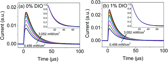 |
| | Fig. 8 Perovskite solar cell transient photocurrent characteristic curves under different light intensities: (a) 0% DIO addition; (b) 1% DIO addition. | |
 |
| | Fig. 9 (a) Dependency of charge extraction on light intensity and (b) dependency of charge extraction time on light intensity for 0% DIO- and 1% DIO-doped perovskite thin films. | |
For further comparing the decreasing tendency of photo-induced current, we normalized the transient photo-induced current curve. The normalization curves are shown in the insets of Fig. 8. The charge extraction time defines photo-induced current attenuation time from the maximum value to 1/e of maximum value. Fig. 9 shows, for the 0% DIO- and 1% DIO-doped perovskite thin film, the dependency of charge extraction time on the light intensity. From Fig. 9, we found that for both devices the extraction time increased with increasing light intensity. However, under the same light intensity, the 1% DIO device's charge extraction time is shorter than that of the 0% DIO device. This indicated that the DIO additive could obviously enhance the charge extraction speed. From Fig. 9(a) and (b), with 1% DIO addition, the device could extract more charge in a short time from the DIO-doped perovskite device, meaning DIO addition could greatly enhance the device's charge transportation and collection ability.
3.3 Additive's effect on the charge recombination process
For exploring how the additive affects the charge recombination mechanism in the perovskite solar cell, we measured the current–voltage curve of the 0% DIO and 1% DIO devices under different light intensities (see Fig. 10). Fig. 10(a) and (b) shows the current–voltage curve of 0% DIO and 1% DIO devices under different light intensities, respectively; Fig. 10(c) and (d) shows normalized I–V characteristic curves of 0% DIO- and 1% DIO-doped devices, respectively. From Fig. 10, we know that the device's total current (Jtotal) is a function of the light intensity (I) and applied voltage (V). It includes the two parts of dark state current (Jdark) and photo-induced current (Jph), namely:21,22| | |
Jtotal(I, V) = Jdark(I, V) + Jph(I, V)
| (1) |
where the photo-induced current can also be expressed as:| | |
Jph(I, V) = qLG(I)PC(I, V)
| (2) |
where q is the elementary charge, L is the active layer's thickness, G(I) is the generating speed of electron–hole pairs in the unit volume, and PC(I, V) is the charge collection probability. Supposing the internal effective electrical field was enough to transport all carriers to the electrode interface, and these charges were collected by the electrode under the appropriate applied reverse bias (−0.2 V), simultaneously, the photo-induced current reached the maximum value, namely reverse saturation current is:
 |
| | Fig. 10 Current–voltage curves of (a) 0% DIO device and (b) 1% DIO device under different light intensities. Normalized I–V characteristic curves of (c) 0% DIO-doped device and (d) 1% DIO-doped device. Two regions are represented on the graph indicating monomolecular and bimolecular recombination. | |
Hence, the PC(I, V) or normalization current relationship can be expressed as:
| |
 | (4) |
Fig. 10(c) shows normalized I–V characteristic curve of 0% DIO-doped device under different light intensities. After normalizing, the curve showed that the device change trend was the same in the −0.2 to 0.4 V range. It showed PC curve change was not connected with the light intensity change; here, the main charge combination was monomolecular recombination. Conversely, when the applied bias voltage was bigger than 0.4 V, when the applied bias voltage further increased, the device internal effective electrical field would decrease, and the collection efficiency of charges would reduce. The PC curve has an obvious dependency relation with the light intensity change, especially near the open-circuit voltage. When Jtotal = 0, the reduction of charge collection ability was the most remarkable; here, the main charge combination was bimolecular recombination. Fig. 10(d) shows the normalized I–V characteristic curve of the 1% DIO-doped device. Compared with the 0% DIO-doped device, in the −0.2 to 0.6 V range, the PC curve has no relation with the light intensity, indicating the main charge combination was monomolecular recombination. But when the voltage changed to the 0.6 V to Voc range, the PC curve has an obvious relation with the light intensity; here, the main charge combination was bimolecular recombination.
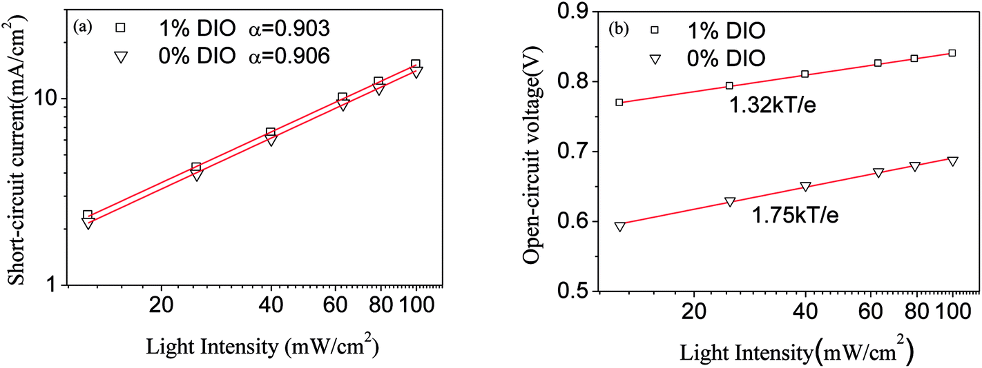
For further understanding the influencing mechanism of the DIO additive on the charge combination process in the perovskite solar cell, and making clear the interrelation of the short-circuit current and the open-circuit voltage and light intensity, the literature reported Jsc and I show following relation:23,24
where
α = 1 indicates the device has a very strong bimolecular recombination action. Taking double logarithms for the short-circuit current and light intensity, we obtain
Fig. 11. Utilizing
eqn (5) to fitting the curve of current-light intensity,
α = 0.903 and
α = 0.906 for the 1% DIO and 0% DIO devices respectively, which are almost equal, but
α = 1, the curve's deviation is biggest, indicating the device exhibited a very strong bimolecular recombination action. Analyzing the above
PC curve, we found that the two devices have a strong obvious dependency relation with the light intensity near open-circuit voltage. They showed a serious combination effect, and therefore we need to further analyze the interrelation between open-circuit voltage and light intensity. When the solar cell is illuminated, the device's open-circuit voltage was equal to the Fermi energy level difference of polymer and fullerene, namely:
25| |
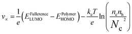 | (6) |
where
ne and
nh are electron and hole concentrations in the fullerene and polymer under open-circuit voltage state, respectively,
Nc is the density of state at energy band edge of fullerene and polymer,
kB is the Boltzmann constant,
T is absolute temperature,
e is the elementary charge,
EPolymerHOMO is the donor polymer ionization potential, and
EFullerenceLUMO is the acceptor fullerene electronic affinity. Transforming
eqn (6) into the relation expression of
Voc and light intensity (
I), we get the equation:
| | |
δVoc = (kBT/e)ln(I) + const
| (7) |
 |
| | Fig. 11 (a) Dependency relation of short-circuit current and light intensity, (b) dependency relation of open-circuit voltage and light intensity in the perovskite solar cell. | |
From the relation of Voc–ln(I), we get δVoc/ln(I) = 2kBT/e, indicating that the device exhibited a serious monomolecular recombination action (trap-assisted recombination). When δVoc/ln(I) = kBT/e, it indicated that the device exhibited a serious bimolecular recombination action. From Fig. 11, the curve of 1% DIO voltage change with the light intensity slope was 1.32kBT/e, indicating that the device exhibited mainly bimolecular recombination near open-circuit voltage. This result supports the previous conclusion, namely, when Voc was bigger than 0.6 V, the recombination process changed from monomolecular recombination to bimolecular recombination for the device with 0% DIO doping. The curve of 1% DIO voltage change with the light intensity slope was 1.75kBT/e. This kind of strong dependency relation of voltage and light intensity indicated the main recombination process was bimolecular recombination and trap-assisted recombination. Because the perovskite has a mass of bulk defects, these defects can act as traps and centers of recombination, and induced the trap to lead to recombination. But the 1% DIO device voltage change with the light intensity slope was small (1.32kBT/e), indicating that the device exhibited a weak trap-induced recombination effect. Therefore, the DIO additive can reduce the trap state-induced recombination in the perovskite solar cell, and enhance the PCE of the perovskite solar cell.
4 Conclusions
In this article, we fabricated a plane structure perovskite solar cell of ITO/PEDOT:PSS/MAPbI3−xClx/PCBM/Al. We utilized the additive DIO to improve the perovskite thin film's morphology quality, and to enhance the perovskite solar cell's efficiency. We studied how the DIO additive affects the charge transportation and collection and recombination physical mechanism by light absorption, surface morphology and potential, capacitance–voltage relation, transient photocurrent, I–V curve under different light intensity, etc. The results are summarized as follows:
(1) When DIO was added to the perovskite, the light absorption intensity of MAPbI3−xClx obviously increased. AFM showed that the surface potential was also obviously increased, indicating that DIO was useful to enhance the thin-film degree of crystallinity, and enhance the perovskite thin film's electrical polarization. C−2–V experimental results found that the 0% DIO- and 1% DIO-doped devices' built-in electrical potentials were 0.63 V and 0.67 V, respectively. Hence, increasing the device's built-in electrical field, and promoting the charge separation and transport lead to an efficiency enhancement from 10.39% to 13.57%.
(2) Transient photo-induced current experiment found that the DIO additive could increase the number of charges extracted, indicating that DIO addition could enhance the charge separation, and produce more charge carriers to be collected by the electrode. In addition, the dependencies of extraction time and light intensity showed that the charge extraction time of the 1% DIO-doped device was smaller than that of the 0% DIO-doped device for the same light intensity, indicating that DIO addition could increase charge extraction speed; namely, it could greatly enhance the charge transportation and collection ability.
(3) The current–voltage curve under different light intensities showed that the 1% DIO and 0% DIO perovskite devices' PC curves have no connection with the light intensity in the range of −0.2 to 0.6 V; here, the main charge recombination was monomolecular recombination in the device. But when the voltage range changed to the 0.6 V to Voc, the PC curve has a strong relation with the light intensity; here, the main charge recombination is bimolecular recombination process. When the recombination process happened near Voc, the slopes of voltage change with light intensity were 1.32kBT/e and 1.75kBT/e for the 1% DIO- and 0% DIO-doped devices, respectively. For the device of 0% DIO doping, the voltage and light intensity have a strong dependency relation showing that the device recombination includes both bimolecular recombination and trap-assisted recombination. We hope these results can be used to promote and help to enhance and develop the high efficiency and stability of perovskite solar cells.
Conflicts of interest
There are no conflicts to declare.
Acknowledgements
We acknowledge financial support from the Hubei Province Natural Science Foundation (grant no. 2016CFB696), Technology Research Programme for Hubei Province Science and Technology Department (grant no. 03201810302) and Breeding Programs Funds for Huanggang Normal University (grant no. 04201813603).
References
- H.-C. Liao, C.-C. Ho, C.-Y. Chang, M.-H. Jao, S. B. Darling and W.-F. Su, Additives for morphology control in high-efficiency organic solar cells, Mater. Today, 2013, 16, 326–336 CrossRef CAS.
- J. N. Joong, N. J. Hong and K. Y. Chan, et al., Solvent engineering for high-performance inorganic–organic hybrid perovskite solar cells, Nat. Mater., 2014, 13, 897–903 CrossRef PubMed.
- J.-H. Im, I.-H. Jang and N. Pellet, et al., Growth of CH3NH3PbI3 cuboids with controlled size for high-efficiency perovskite solar cells, Nat. Nanotechnol., 2014, 9, 927–932 CrossRef CAS PubMed.
- L. P. Peng and Z. T. Liu, Reduce the hysteresis effect with the PEIE interface dipole effect in the organic–inorganic hybrid perovskite CH3NH3PbI3−xClx solar cell, Org. Electron., 2018, 6, 043, DOI:10.1016/j.orgel.2018.06.043.
- M. S. Su, C. Y. Kuo and M.-C. Yuan, et al., Improving device efficiency of polymer/fullerene bulk heterojunction solar cells through enhanced crystallinity and reduced grain boundaries induced by solvent additives, Adv. Mater., 2011, 23, 3315–3319 CrossRef CAS.
- J. Peet, J. Y. Kim and N. E. Coates, et al., Efficiency enhancement in low-band gap polymer solar cells by processing with alkane dithiols, Nat. Mater., 2007, 6, 497–500 CrossRef CAS PubMed.
- P. W. Liang, C. Y. Liao and C. C. Chueh, et al., Additive enhanced crystallization of solution-processed perovskite for highly efficient planar-heterojunction solar cells, Adv. Mater., 2014, 26, 3748–3754 CrossRef CAS PubMed.
- R. Adharsh, K. Yao and K.-Y. J. Alex, Toward Perovskite Solar Cell Commercialization: A Perspective and Research Roadmap Based on Interfacial Engineering, Adv. Mater., 2018, 30, 1800455 CrossRef PubMed.
- A. Solh, C. H. Wang, C. H. Cao, C. J. Zhang, J. L. Yang and L. Jiang, Improvement of CH3NH3PbI3 thin film using the additive 1,8-diiodooctane for planar heterojunction perovskite cells, Phys. B, 2017, 522, 43–47 CrossRef.
- A. Foertig, J. Kniepert and M. Gluecker, et al., Nongeminate and geminate recombination in PTB7:PCBM solar cells, Adv. Funct. Mater., 2014, 24, 1306–1311 CrossRef CAS.
- S. R. Cowan, B. Natalie and W. L. Leong, et al., Charge formation, recombination, and sweep-out dynamics in organic solar cells, Adv. Funct. Mater., 2012, 22, 1116–1128 CrossRef CAS.
- A. Pivrikas, G. Juška and A. J. Mozer, et al., Bimolecular recombination coefficient as a sensitive testing parameter for low-mobility solar-cell materials, Phys. Rev. Lett., 2005, 94, 176806 CrossRef CAS PubMed.
- S. R. Cowan, W. L. Leong and B. Natalie, et al., Identifying a threshold impurity level for organic solar cells: enhanced first-order recombination via well-defined PC84BM traps in organic bulk heterojunction solar cells, Adv. Funct. Mater., 2011, 21, 3083–3092 CrossRef CAS.
- G.-B. Germà and B. Juan, Open-circuit voltage limit caused by recombination through tail states in bulk heterojunction polymer-fullerene solar cells, Appl. Phys. Lett., 2010, 96, 113301 CrossRef.
- A. J. Mozer, G. Dennler and N. S. Sariciftci, et al., Time-dependent mobility and recombination of the photoinduced charge carriers in conjugated polymer/fullerene bulk heterojunction solar cells, Phys. Rev. B: Condens. Matter Mater. Phys., 2005, 72, 035217 CrossRef.
- M. H. Tong, N. E Coates and D. Moses, et al., Charge carrier photogeneration and decay dynamics in the poly(2,7-carbazole) copolymer PCDTBT and in bulk heterojunction composites with PC70BM, Phys. Rev. B: Condens. Matter Mater. Phys., 2010, 81, 125210 CrossRef.
- S. R. Cowan, R. A. Street and S. Cho, et al., Transient photoconductivity in polymer bulk heterojunction solar cells: competition between sweep-out and recombination, Phys. Rev. B: Condens. Matter Mater. Phys., 2011, 83, 035205 CrossRef.
- L. J. A. Koster, M. Kemerink and M. M. Wienk, et al., Quantifying bimolecular recombination losses in organic bulk heterojunction solar cells, Adv. Mater., 2011, 23, 1670–1674 CrossRef CAS PubMed.
- C. H. Cao, C. J. Zhang, J. L. Yang, J. Sun, S. P. Pang, H. Wu, R. S. Wu, Y. L. Gao and C. B. Liu, Iodine and Chlorine Element Evolution in CH3NH3PbI3−xClx Thin Films for Highly Efficient Planar Heterojunction Perovskite Solar Cells, Chem. Mater., 2016, 28(8), 2742–2749 CrossRef CAS.
- X. Song, W. W. Wang, P. Sun, W. L. Ma and Z.-K. Chen, Additive to regulate the perovskite crystal film growth in planar heterojunction solar cells, Appl. Phys. Lett., 2015, 106, 033901 CrossRef.
- D. H. Wang, A. Kyaw and K. Ko, Roles of solvent additive in organic photovoltaic cells through intensity dependence of current–voltage characteristics and charge recombination, Appl. Phys. Lett., 2014, 105, 103301 CrossRef.
- Y. P. Peng, Y. D. Cheng, C. H. Wang, C. J. Zhang and J. L. Yang, Fully doctor-bladed planar heterojunction perovskite solar cells under ambient condition, Org. Electron., 2018, 58, 153–158 CrossRef CAS.
- B. Y. Qi and J. Z. Wang, Open-circuit voltage in organic solar cells, J. Mater. Chem., 2012, 22, 24315–24325 RSC.
- I. Riedel, J. Parisi and V. Dyakonov, et al., Effect of temperature and illumination on the electrical characteristics of polymer-fullerene bulk-heterojunction solar cells, Adv. Funct. Mater., 2004, 14, 38–44 CrossRef CAS.
- P. Schilinsky, C. Waldauf and C. J. Brabec, Recombination and loss analysis in polythiophene based bulk heterojunction photodetectors, Appl. Phys. Lett., 2002, 81, 3885–3887 CrossRef CAS.
|
| This journal is © The Royal Society of Chemistry 2018 |
Click here to see how this site uses Cookies. View our privacy policy here. 
 Open Access Article
 This Open Access Article is licensed under a Creative Commons Attribution-Non Commercial 3.0 Unported Licence
 *ab,
Wei Xiea and
Changquan Yanga
*ab,
Wei Xiea and
Changquan Yanga