
 Open Access Article
 This Open Access Article is licensed under a
 Creative Commons Attribution 3.0 Unported Licence
Na–Ga–Si type-I clathrate single crystals grown via Na evaporation using Na–Ga and Na–Ga–Sn fluxes†
Hironao Urushiyamaa,
Haruhiko Morito *b,
Hisanori Yamanea and
Masami Terauchia
*b,
Hisanori Yamanea and
Masami Terauchia
aInstitute of Multidisciplinary Research for Advanced Materials, Tohoku University, 2-1-1 Katahira, Aoba-ku, Sendai 980-8577, Japan
bInstitute for Materials Research, Tohoku University, 2-1-1 Katahira, Aoba-ku, Sendai 980-8577, Japan. E-mail: morito@imr.tohoku.ac.jp
First published on 4th December 2018
Abstract
Single crystals of a Na–Ga–Si clathrate, Na8Ga5.70Si40.30, of size 2.9 mm were grown via the evaporation of Na from a Na–Ga–Si melt with the molar ratio of Na![[thin space (1/6-em)]](https://www.rsc.org/images/entities/char_2009.gif) :Ga:Si = 4:1:2 at 773 K for 21 h under an Ar atmosphere. The crystal structure was analyzed using X-ray diffraction with the model of the type-I clathrate (cubic, a = 10.3266(2) Å, space group Pm
:Ga:Si = 4:1:2 at 773 K for 21 h under an Ar atmosphere. The crystal structure was analyzed using X-ray diffraction with the model of the type-I clathrate (cubic, a = 10.3266(2) Å, space group Pm![[3 with combining macron]](https://www.rsc.org/images/entities/char_0033_0304.gif) n, no. 223). By adding Sn to a Na–Ga–Si melt (Na:Ga:Si:Sn = 6:1:2:1), single crystals of Na8GaxSi46−x (x = 4.94–5.52, a = 10.3020(2)–10.3210(3) Å), with the maximum size of 3.7 mm, were obtained via Na evaporation at 723–873 K. The electrical resistivities of Na8Ga5.70Si40.30 and Na8Ga4.94Si41.06 were 1.40 and 0.72 mΩ cm, respectively, at 300 K, and metallic temperature dependences of the resistivities were observed. In the Si L2,3 soft X-ray emission spectrum of Na8Ga5.70Si40.30, a weak peak originating from the lowest conduction band in the undoped Si46 was observed at an emission energy of 98 eV.
n, no. 223). By adding Sn to a Na–Ga–Si melt (Na:Ga:Si:Sn = 6:1:2:1), single crystals of Na8GaxSi46−x (x = 4.94–5.52, a = 10.3020(2)–10.3210(3) Å), with the maximum size of 3.7 mm, were obtained via Na evaporation at 723–873 K. The electrical resistivities of Na8Ga5.70Si40.30 and Na8Ga4.94Si41.06 were 1.40 and 0.72 mΩ cm, respectively, at 300 K, and metallic temperature dependences of the resistivities were observed. In the Si L2,3 soft X-ray emission spectrum of Na8Ga5.70Si40.30, a weak peak originating from the lowest conduction band in the undoped Si46 was observed at an emission energy of 98 eV.
1. Introduction
Na8Si46 type-I clathrate has an open framework structure composed of dodecahedral [Si]20 cages with five-membered rings of Si [512] and tetrakaidecahedral [Si]24 cages with five-membered rings and six-membered rings of Si [51262].1 Each cage encapsulates a Na as a guest atom. Since this compound was first synthesized by Kasper et al. in 1965,1 it has attracted significant attention from researchers owing to its unique structure as well as being a member of group 14 intermetallic chathrates, the variants of which are of interest for photovoltaic,2 thermoelectric,3 and superconducting materials.4Na8Si46 has conventionally been synthesized along with another type of Na–Si clathrate (type-II, Na24Si36) via the solid-thermal decomposition of Na4Si4 (melting point 1071 K (ref. 5)) in the temperature range 593–823 K under high vacuum (<10−2 Pa).1,6,7 The samples obtained by this method are powdery solids with a grain size of micrometers. The Na–Si clathrates have been regarded as metastable or intermediate phases. The single crystals of Na8Si46 could not be directly grown from the Na–Si melt. In 2009, Beekman et al. succeeded in growing type-II Na24Si136 single crystal growth using a spark plasma sintering (SPS) system.8 Single crystals of type-I and type-II clathrates were selectively synthesized by the reaction of Na4Si4 and graphite flakes with a spatial separation layer of NaCl.9,10 This process was named the kinetically controlled thermal decomposition (KCTD) method. Type-I Na8Si46 single crystal with sizes of about 200 μm was obtained by heating at 858 K.9 Recently, our research group found that the single crystal of the Na–Si binary clathrates can be grown in Na–Sn rich Na–Sn–Si ternary melt by Na evaporation.11,12 Single crystals of type-I and type-II clathrates were selectively prepared by setting the growth temperatures at 773 and 873 K, respectively. The maximum size of the type-I Na8Si46 single crystal was 5 × 3 × 3 mm3, having {110} habit planes.12
The electric properties of ternary type-I clathrates A8M8Si38 (A = Na, K, Rb, Cs; M = Al, Ga, In) have been predicted using first-principles calculation.13,14 Indirect transition semiconductor characters of A8M8Si38 with band gaps of 0.45–0.89 eV13 and their thermoelectric properties14 were presented by the calculation. A8Al8Si38 (A = K, Rb, Cs) have been synthesized using flux materials of Al and alkali-metal halide salts.15 The samples for the transport measurements were prepared by compacting at 4 GPa in a high-pressure multianvil apparatus. Dong et al. synthesized microcrystalline Na8Al8Si38 by the KCTD method using a Na4Si4 + NaAlSi mixture as the precursor and prepared bulk polycrystalline samples by SPS to characterize the transport properties.16 Sui et al. synthesized A8Ga8Si38 (A = K, Rb, Cs) via a direct reaction of constituent elements.17 They sintered the powders of A8Ga8Si38 using SPS to obtain polycrystalline bulk samples for characterization of thermoelectric properties, and measured the band gaps of 1.14–1.18 eV by the surface electromotive force of the powder samples.17 A cubic lattice parameter of 10.36 Å was only reported for Na8Ga23Si23,18 but details of synthesis and crystal structures of the clathrates have not been clarified. The present paper reports crystal growth of the type-I clathrate Na8Ga5.70Si40.30 using a Na–Ga–Si melt and Na8GaxSi46−x (x = 4.94–5.52) using Na–Ga–Si–Sn melts. The crystal structures were analyzed by single crystal X-ray diffraction (XRD) and some single crystals were characterized by electrical resistivity measurement and soft X-ray emission spectroscopy (SXES).
2. Experimental
As starting raw materials, Na (Nippon Soda Co., Ltd., purity 99.95%), Si powder (Kojundo Chemical Laboratory Co., Ltd., 4N), granular Ga (Dowa Electronics Co., 6N), and granular Sn (Mitsuwa Chemicals Co., Ltd., 5N) were used. These raw materials were weighed in a molar ratio of Na:Ga:Si = 4:1:2 (total 12.19 mmol) or Na:Ga:Si:Sn = 6:1:2:1 (total 8.70 mmol) in an Ar-filled glove box. They were placed in a boron nitride crucible (Showa Denko Co., Ltd., purity 99.95%, outer diameter 8.5 mm, inner diameter 6.5 mm, depth 18 mm) and sealed in a stainless-steel container (SUS 316: outer diameter 12.7 mm, inner diameter 10.7 mm, height 80 mm) together with Ar gas. The crucible was heated in an electric furnace at 1123 K for 12 h, and thereafter cooled to room temperature to prepare the starting sample of Na–Ga–Si or Na–Ga–Si–Sn.
The crucible containing the starting sample was taken out from the stainless-steel container in the glove box under Ar atmosphere, and transferred to the upper part of another long stainless-steel container (outer diameter 12.7 mm, inner diameter 10.7 mm, height 300 mm). A schematic view of the container is shown in Fig. S1 of ESI.† The crucible at the upper part of the container was heated at 723–873 K for 3–24 h in atmospheric-pressure Ar using a tubular electric furnace, and the lower part of the container was cooled with a fan to maintain a temperature gradient in the container. Na evaporated from the melt of the starting sample was condensed at the lower inside part of the container. After heating, the sample was cooled to room temperature by turning off the electric power to the furnace and taken out the sample from the container in the glove box. The amount of evaporated Na was evaluated using the weight loss of the sample after heating. Unvaporized Na and Na–Ga, Na–Si, and/or Na–Sn compounds formed in the sample were reacted with 2-propanol and ethanol in air, and subsequently, the water-soluble reactants were removed by washing with water. Single crystals were obtained after the removal of residual Ga and Sn via a reaction with hydrochloric acid water solution (35.0–37.0 mass% HCl) (alcohol and acid treatments).
Caution: confirm the complete decomposition of the reactive compounds containing Na through reaction with alcohol before washing with water.
The compositions of the single crystals were analyzed using an electron probe microanalyzer (EPMA, JEOL, JXA-8200) attached to wavelength dispersive X-ray spectrometers. The densities of the single crystals were measured using the Archimedes method. The X-ray diffraction (XRD) data of the single crystals were collected using a single-crystal XRD diffractometer (Bruker, D8QUEST, Mo-Kα radiation) and analyzed using the APEX3 program.19 X-ray absorption correction and structure refinement were performed by using the SADABS19 and SHELEXL-97 programs,20 respectively. The structures of Si/Ga cages containing Na were depicted using VESTA.21 Soft X-ray emission (SXE) spectra were measured using an SXE spectrometer attached to a port of a wavelength-dispersive spectrometer of a scanning electron microscope (SEM, JEOL, JSM-6480LV22,23). The electric resistivities of the single crystals were measured from 10 to 300 K using the four-terminal method with Ag paste electrodes.
3. Results and discussion
The conditions of crystal growth and mole fractions of the evaporated Na against the initial amounts of Na in the starting samples are listed in Table 1. It can be observed that 84% of Na was evaporated during the heating of Na–Ga–Si starting sample at 773 K for 21 h. Single crystals of size up to 2.9 mm were obtained. When the Na–Ga–Si–Sn starting samples were heated at 723 K for 24 h, 773 K for 12 h, 823 K for 9 h, and 873 K for 3 h, 48–55% of Na was evaporated. Fig. 1 shows an optical micrograph of the single crystals grown by heating the Na–Ga–Si–Sn starting sample at 873 K for 3 h. The maximum sizes of the single crystals grown at 723, 773, 823, and 873 K were 2.3, 2.5, 2.6, and 3.7 mm, respectively.| Sample | Composition of the starting sample | Temp. (K) | Time (h) | Evaporated Na (mol mol−1) | Crystal size (mm) |
|---|---|---|---|---|---|
| Na:Ga:Si |
|||||
| 1 | 4:1:2 |
773 | 21 | 0.84 | 2.9 |
|
|||||
| Na:Ga:Si:Sn |
|||||
| 2 | 6:1:2:1 |
723 | 24 | 0.49 | 2.3 |
| 3 | 6:1:2:1 |
773 | 12 | 0.50 | 2.5 |
| 4 | 6:1:2:1 |
823 | 9 | 0.48 | 2.6 |
| 5 | 6:1:2:1 |
873 | 3 | 0.55 | 3.7 |
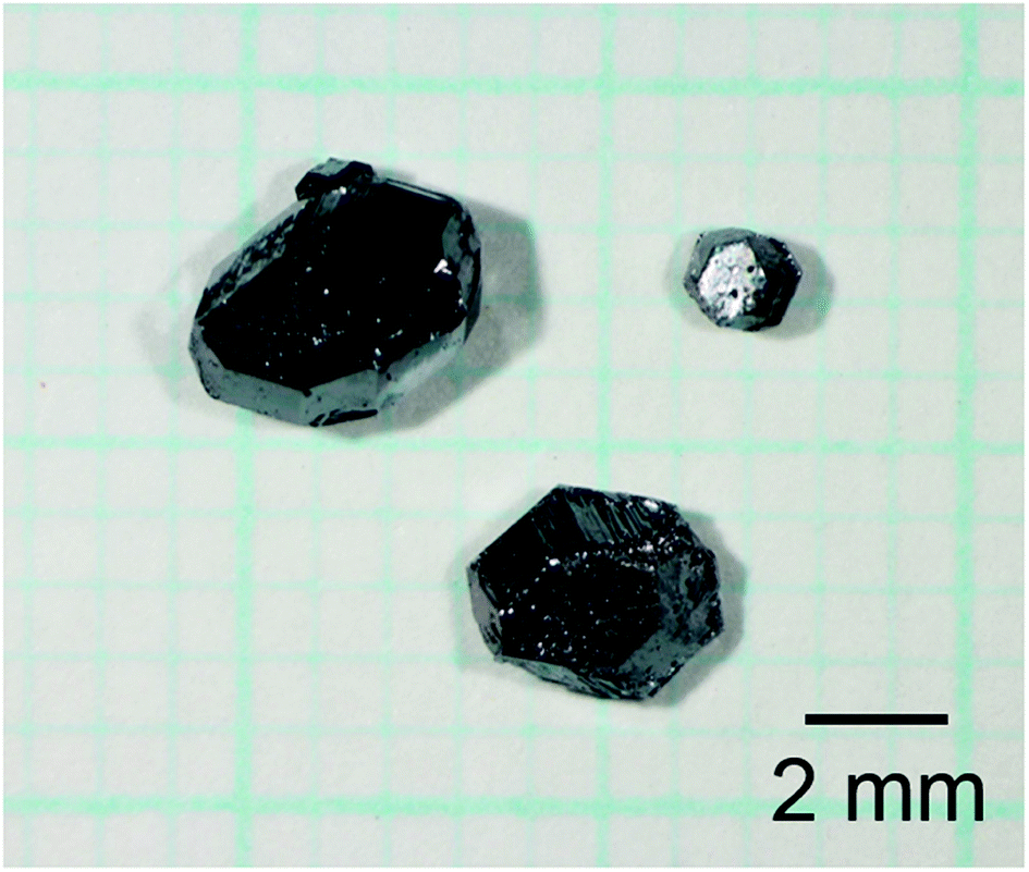 | ||
| Fig. 1 Optical micrographs of the single crystals grown via Na evaporation from the Na–Ga–Si–Sn starting sample at 873 K for 3 h under an Ar atmosphere (∼105 Pa), followed by alcohol and acid treatments. | ||
Table 2 shows the compositions of the single crystals grown by heating the Na–Ga–Si starting sample at 773 K (crystal 1) and the Na–Ga–Si–Sn starting samples at 723 (crystal 2), 773 (crystal 3), 823 (crystal 4), and 873 K (crystal 5). Elements other than Na, Ga, and Si were not detected from these crystals using EPMA. When the total number of the Ga and Si cage atoms was set to 46, based on the ideal formula of type-I clathrates Na8GaxSi46−x, the contents of Na analyzed using EPMA were converted from 7.99(6) to 8.23(6), which is close to the ideal Na number of 8. The Ga number of crystal 1 grown at 773 K from the Na–Ga–Si starting sample was 5.67(8). The Ga numbers x of Na8GaxSi46−x for crystals 2, 3, 4, and 5 grown from the Na–Ga–Si–Sn starting mixture were 5.41(3), 5.35(3), 5.19(6), and 4.78(3) respectively, which decreased with the increase in the heating temperature from 723 to 873 K as shown in Fig. 2.
| Chemical composition | ||||
|---|---|---|---|---|
| Na (at%) | Ga (at%) | Si (at%) | Chemical formula based on Si + Ga = 46 | |
| 1 | 14.91(10) | 10.48(15) | 74.6(2) | Na8.06(6)Ga5.67(8)Si40.33(13) |
| 2 | 14.99(12) | 10.00(6) | 75.01(12) | Na8.11(6)Ga5.41(3)Si40.59(6) |
| 3 | 15.03(5) | 9.88(5) | 75.09(9) | Na8.14(3)Ga5.35(3)Si40.65(5) |
| 4 | 15.18(12) | 9.58(12) | 75.3(2) | Na8.23(6)Ga5.19(6)Si40.81(12) |
| 5 | 14.79(11) | 8.85(6) | 76.36(17) | Na7.99(6)Ga4.78(3)Si41.22(9) |
 | ||
| Fig. 2 Ga content of type-I clathrates Na8GaxSi46−x versus heating temperatures of Na–Ga–Si mixture (△) and Na–Ga–Si–Sn mixtures (●). | ||
The results of crystal structure analysis and refined atomic positional and equivalent isotropic displacement parameters of the single crystals are shown in Tables 3 and S1.† All the single crystals were analyzed with the type-I structure (cubic system, space group Pmn). In the structure refinements, Na1(6d) and Na2(2a) sites were fully occupied and the occupancies of Ga in Si/Ga1(24k), Si2(16i), and Si/Ga3(6c) sites were refined. As the occupancy of the Si2(16i) site equaled 1 within the standard deviation, it was fixed to 1 in the final refinements. The reliability factors R1 (all data) for samples 1–5 were 1.02–1.90%. The formulae of the clathrates based on the refined occupancies were in accordance with those determined using EPMA. The a-axis length of Na8GaxSi46−x increased from 10.3020(2) to 10.3226(2) Å with the increase in the Ga content x from 4.94(6) to 5.70(7) as shown in Fig. 3(a). The densities in the range 2.554–2.584 Mg m−3, which were calculated using the lattice parameters and the formulas, were consistent with those measured using the Archimedes method (Table 3).
| a R1 = Σ||Fo| − |Fc||/Σ|Fo|. wR2 = [Σw(Fo2 − Fc2)2/Σ(wFo2)2]1/2, w = 1/[σ2(Fo2) + (aP)2 + bP], where Fo is the observed structure factor, Fc is the calculated structure factor, σ is the standard deviation of Fc2, and P = (Fo2 + 2Fc2)/3. S = [Σw(Fo2 − Fc2)2/(n − p)]1/2, where n is the number of reflections and p is the total number of parameters refined. | |||||
|---|---|---|---|---|---|
| Crystal | 1 | 2 | 3 | 4 | 5 |
| Chemical formula | Na8Ga5.70(7)Si40.30 | Na8Ga5.52(7)Si40.48 | Na8Ga5.39(11)Si40.61 | Na8Ga5.06(7)Si40.94 | Na8Ga4.94(6)Si41.06 |
| Formula weight, Mr (g mol−1) | 1713.35 | 1705.86 | 1700.37 | 1686.71 | 1681.71 |
| Temperature, T (K) | 298(2) | 302(2) | 302(2) | 300(2) | 300(2) |
| Crystal system | Cubic | Cubic | Cubic | Cubic | Cubic |
| Space group | Pmn |
Pmn |
Pmn |
Pmn |
Pmn |
| Unit-cell dimensions, a (Å) | 10.3266(2) | 10.3210(3) | 10.3210(4) | 10.3090(2) | 10.3020(2) |
| Unit-cell volume, V (Å3) | 1101.21(4) | 1099.42(6) | 1099.42(7) | 1095.59(4) | 1093.36(6) |
| Z | 1 | 1 | 1 | 1 | 1 |
| Measured density, Dobs (Mg m−3) | 2.584(1) | 2.561(9) | 2.563(2) | 2.541(5) | 2.514(5) |
| Calculated density, Dcal (Mg m−3) | 2.584 | 2.576 | 2.568 | 2.556 | 2.554 |
| Radiation wavelength, l (Å) | 0.71073 | 0.71073 | 0.71073 | 0.71073 | 0.71073 |
| Size (mm) | 0.125 × 0.177 × 0.188 | 0.163 × 0.126 × 0.124 | 0.207 × 0.130 × 0.124 | 0.246 × 0.214 ×0.168 | 0.253 × 0.193 × 0.153 |
| Absorption correction | Multi-scan | Multi-scan | Multi-scan | Multi-scan | Multi-scan |
| Absorption coefficient, μ (mm−1) | 4.635 | 4.540 | 4.464 | 4.291 | 4.231 |
| Limiting indices | −9 ≤ h ≤ 11 | −5 ≤ h ≤ 13 | −13 ≤ h ≤ 10 | −11 ≤ h ≤ 12 | −6 ≤ h ≤ 13 |
| −13 ≤ k ≤ 9 | −12 ≤ k ≤ 8 | −11 ≤ k ≤ 11 | −13 ≤ k ≤ 6 | −11 ≤ k ≤ 11 | |
| −13 ≤ l ≤ 11 | −10 ≤ l ≤ 13 | −13 ≤ l ≤ 6 | −9 ≤ l ≤ 13 | −12 ≤ l ≤ 13 | |
| F000 | 829 | 826 | 824 | 818 | 816 |
| θ range for date collection, ° | 2.790–27.414 | 2.791–27.430 | 2.791–27.430 | 2.794–27.464 | 2.796–27.484 |
| Reflections collected/unique | 2738/252 | 2594/250 | 2618/250 | 2586/249 | 2581/250 |
| Rint | 0.0234 | 0.0264 | 0.0292 | 0.0263 | 0.0265 |
| Date/restraints/parameters | 250/0/18 | 250/0/18 | 250/0/18 | 249/0/18 | 250/0/18 |
| Weight parameters, a, b | 0.0164, 0.2950 | 0.0141, 0.1813 | 0.0187, 0.7742 | 0.0151, 0.1907 | 0.0110, 0.2230 |
| Goodness-of-fit on F2, S | 1.153 | 1.188 | 1.248 | 1.232 | 1.296 |
| R1, wR2 (I > 2s(I)) | 0.0118, 0.0304 | 0.0120, 0.0307 | 0.0176, 0.0427 | 0.0106, 0.0299 | 0.0100, 0.0269 |
| R1, wR2 (all data) | 0.0125, 0.0309 | 0.0127, 0.0311 | 0.0190, 0.0442 | 0.0108, 0.0300 | 0.0102, 0.0269 |
| Largest diff. peak and hole, Δr (e Å−3) | 0.300, −0.244 | 0.298, −0.176 | 0.374, −0.292 | 0.244, −0.133 | 0.381, −0.200 |
 | ||
| Fig. 3 Plots of a-axis length (a), 6c and 24k site occupancies of Ga (b), and normalized volumes of [Si/Ga]24 cage and [Si/Ga]20 cage (c) versus Ga content x of Na8GaxSi46−x. | ||
The Na2-centered [Si/Ga]20 and Na1-centered [Si/Ga]24 cages of Na8Ga5.70Si40.30 are shown in Fig. 4(a). The occupancies of Ga in the Si/Ga1(24k) and Si/Ga3(6c) sites are plotted against the Ga content x in Fig. 3(b). The Si/Ga3 site, constituting six-membered rings of the [Si/Ga]24 cage, was preferentially occupied by Ga atoms with occupancies in the range 64.8(3)–73.0(4)%. The volume increasing rate of the [Si/Ga]24 cage is larger than that of the [Si/Ga]20 cage (Fig. 3(c)). Similar Ga preferential occupation of the Si/Ga3 site in the [Si/Ga]24 cages, which prevents Ga–Ga atom contact, was previously reported for A8Ga8Si38 (A = K, Rb, Cs) type-I clathrate.17
 | ||
| Fig. 4 [Si/Ga]20 and [Si/Ga]24 cages of Na8Ga5.70Si40.30 depicting with spheres of occupancies (a) and 99% probability displacement ellipsoids (b). | ||
In Fig. 4(b), the atomic arrangement of Na8Ga5.70Si40.30 is shown with 99% probability ellipsoids using the anisotropic atomic displacement parameters (Table S2†). The ellipsoids of the Si and Si/Ga sites are small and close to spherical. The atomic displacement parameters of the Na2 site at the center of the [Si/Ga]20 regular dodecahedron (U11 = U22 = U33: 0.0229(5)–0.2038(6) Å2) are approximately four times larger than those of the Si and Si/Ga sites. The parameters of U22 = U33(0.0715(9) − 0.0787(11) Å2) for the Na1 site in the [Si/Ga]24 cages are the largest in each structure, indicating large displacement of Na atoms at the Na1 site in the direction parallel to the six-membered ring of the Si/Ga1 and Si/Ga3 sites.
Dong et al. reported the preparation of Na8Al8Si38 using SPS and a linear relationship between the a-axis lengths of A8Al8Si38 (A = Na, K, Rb, Cs, Ba) and the ionic radii (coordination number CN = 12) of A.16 In the present study, the highest Ga content x of Na8GaxSi46−x was 5.70(7), whereas A8Ga8Si38 (x = 8) was reported for other alkali elements A = K, Rb, and Cs.17 However, the a-axis lengths of Na8Ga5.70Si40.30 and these type-I gallium silicon clathrates are plotted on the same line against the ionic radii of the alkali metals as shown in Fig. 5. The a-axis lengths of A8Ga8Si38, A = K, Rb, and Cs, are smaller than the corresponding values of A8Al8Si38, but the lengths of Na8Al8Si38 (10.3260(1) Å) and Na8Ga5.70Si40.30 (10.3266(2) Å) are similar. As there is a linear relation between the a-axis length of Na8GaxSi46−x and x, the a-axis length of hypothetical Na8Ga8Si36 could be estimated to be 10.375 Å via extrapolation (Fig. 3(a)). The length is plotted out of the line in the graph shown in Fig. 5. Although it is not apparent whether Na8Ga8Si36 was formed at this moment, there might be an upper size limit of cages containing Na atoms in the type-I clathrate structure. Thus, a high-pressure condition may be required to crystalize Na8Ga8Si38.
 | ||
| Fig. 5 Plot of a-axis length versus ionic radius (coordination number 12) of the guest atoms for Na8Si46,11 Na8Ga5.7Si40.3 and A8(Al/Ga)8Si38 (A = Na, K, Rb, and Cs).15–17 The hypothetical a-axis length of Na8Ga8Si38 estimated in Fig. 3(a) is also plotted with ×. | ||
Fig. 6 shows the SXE spectra of crystal 1 (Na8Ga5.70Si40.30), Na–Si binary type-I clathrate (Na8Si46) synthesized in the previous study,11 and diamond-type cubic Si (d-Si), which was the same as the starting material. The peaks observed around 99 and 98 eV in the spectra of Na8Si46 and Na8Ga5.70Si40.30 are consistent with the peak observed at 99 eV for Na8Si46 by Moewes et al.24 It was considered that the peak edges corresponded to the lower end of the conduction band where the Fermi level exists. Although the peak of 99 eV with a sharp edge at 101 eV was observed for Na8Si46, the corresponding peak of Na8Ga5.70Si40.30 was small, which indicates the difference between the electronic states of these clathrates.
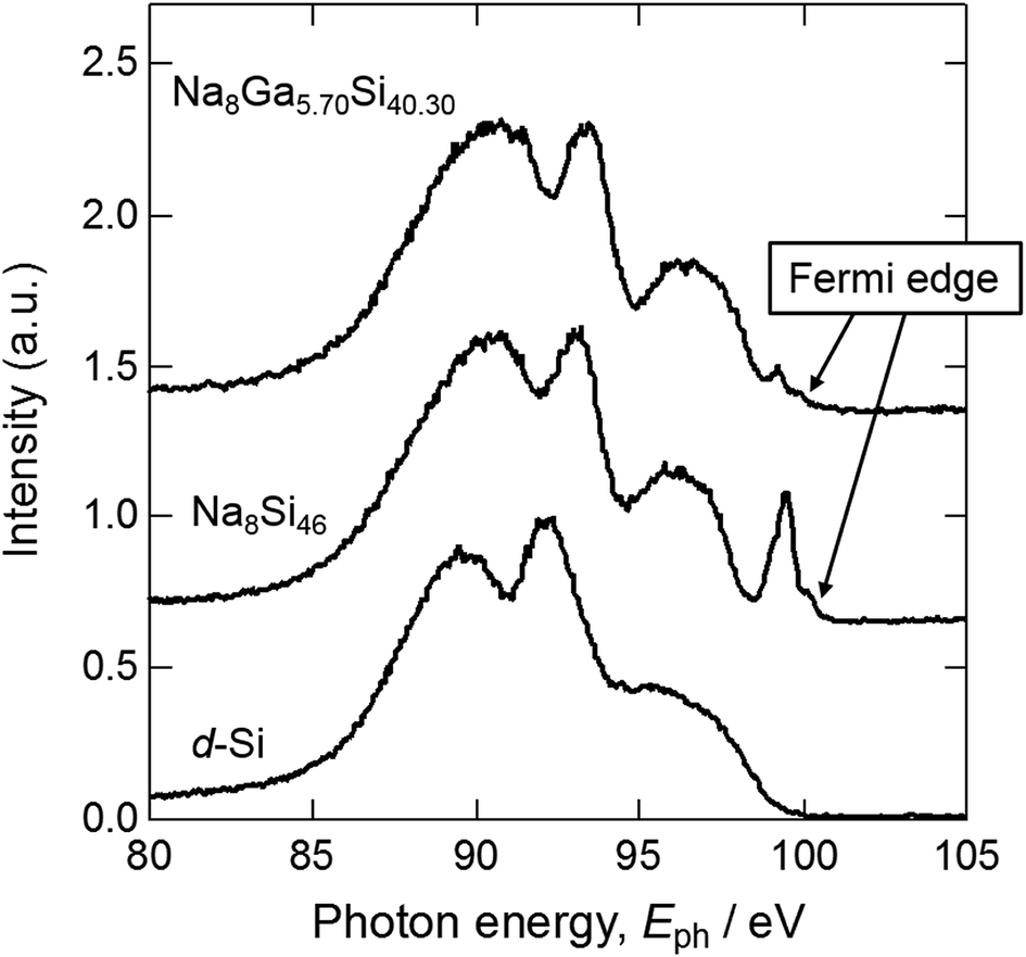 | ||
| Fig. 6 Si L2,3 SXE spectra of Na8Ga5.70Si40.30, Na8Si46, and d-Si. | ||
The peak observed around 93–94 eV in the Na8Si46 spectrum shifted higher by approximately 0.5 eV from that of the d-Si. The peak of Na8Ga5.70Si40.30 was further shifted by approximately +0.3 eV from that of Na8Si46. The Si–Si distances of d-Si and Na8Si46, and the Si/Ga–Si/Ga distance of Na8Ga5.70Si40.30 were 2.35166 Å,25 2.3286(11)–2.3941(9) Å,11 and 2.3610(10)–2.4370(4) Å (Table S3†), respectively. As the Si–Si or Si/Ga–Si/Ga distance increases, the band gap decreases. Consequently, the energy gaps between the inner shell levels and valence band increase and the spectra shift to the higher energy side.
The electrical resistivities measured for crystal 1 (Na8Ga5.70Si40.30) and crystal 5 (Na8Ga4.94Si41.06) together with the resistivity of Na8Si46 (ref. 11) are shown against the temperature in Fig. 7. These crystals showed metallic behavior. The electrical resistivity decreased as the Ga content decreased, and those of Na8Ga5.70Si40.30 and Na8Ga4.94Si41.06 at 300 K were 1.40 and 0.72 mΩ cm, respectively. These values were greater than the resistivity of Na8Si46 (0.24 mΩ cm at 300 K (ref. 11)). In the case of Na8Si46, most electrons supplied from Na to the Si cage remain in the conduction band and contribute to the metallic conduction. When a part of tetravalent Si atoms is replaced by trivalent Ga atoms, some electrons from the Na atoms are present in the valence band owing to the decrease in the valence electrons through Ga substitution.
 | ||
| Fig. 7 Temperature dependence of electrical resistivity for single crystals of Na8Ga5.70Si40.30, Na8Ga4.94Si41.06, and Na8Si46.11 | ||
A8Ga8Si38 (A = K, Rb, Cs) synthesized by Sui et al.17 are semiconductors, exhibiting a decrease in the electrical resistivities with an increase in temperature. This is attributed to the fact that the number of electrons provided by A atoms is the same as the number of valence electrons decreased through substitution of Ga for Si atoms in the cage, which fulfills the octet condition. The first-principle calculation by Imai et al.13 predicted that Na8Ga8Si38 is a semiconductor with a band gap of 0.448 eV. As the maximum Ga content x = 5.70(7) of Na8GaxSi46−x synthesized in the present study is less than 8, the surplus electrons from Na remain in the conduction band and contribute to the metallic conduction as in the case of Na8Si46. Similar metallic conduction was also reported for K8Al7Si39.26,27 Dong et al. suggested that the Al content of x would be slightly less than 8 for Na8Al8Si38, judging from the weak temperature dependence of electrical conductivity with a small activation energy.16
4. Conclusions
Single crystals of novel Na–Ga–Si ternary type-I clathrates were successfully grown by evaporating Na from a Na–Ga–Si or Na–Ga–Si–Sn melt. A single crystal of Na8Ga5.70Si40.30 of size 2.9 mm was obtained from the Na–Ga–Si melt by heating at 773 K for 21 h. The Ga content x of Na8GaxSi46−x single crystals grown from the Na–Ga–Si–Sn melt decreased from 5.52 to 4.94 with the increase in the heating temperature from 723 to 873 K. The size of a Na8Ga4.94Si41.06 single crystal grown from the Na–Ga–Si–Sn melt at 873 K was 3.7 mm. The metallic temperature dependences of the electric resistivities expected from the formula of Na8GaxSi46−x (x = 5.70, 4.94) were confirmed for the single crystals.Conflicts of interest
There are no conflicts to declare.Acknowledgements
The authors would like to thank T. Kamaya for EPMA analysis. This work was supported by JSPS KAKENHI Grant Number JP16H06123.Notes and references
- J. S. Kasper, P. Hagenmuller, M. Pouchard and C. Cros, Science, 1965, 150, 1713 CrossRef CAS PubMed.
- G. B. Adams, M. O'Keeffe, A. A. Demkov, O. F. Sankey and Y.-M. Huang, Phys. Rev. B, 1994, 49, 8048 CrossRef CAS.
- J.-A. Dolyniuk, B. Owens-Baird, J. Wang, J. V. Zaikina and K. Kovnir, Mater. Sci. Eng. R Rep., 2016, 108, 1 CrossRef.
- H. Kawaji, H. Horie, S. Yamanaka and M. Ishikawa, Phys. Rev. Lett., 1995, 74, 1427 CrossRef CAS PubMed.
- H. Morito, T. Yamada, T. Ikeda and H. Yamane, J. Alloys Compd., 2009, 480, 723 CrossRef CAS.
- C. C. M. Pouchard, C. R. Chim., 2009, 12, 1014 CrossRef.
- H. Horie, T. Kikudome, K. Teramura and S. Yamanaka, J. Solid State Chem., 2009, 182, 129 CrossRef CAS.
- M. Beekman, M. Baiitinger, H. Borrmann, W. Schnelle, K. Meier, G. S. Nolas and Y. Grin, J. Am. Chem. Soc., 2009, 131, 9642 CrossRef CAS PubMed.
- S. Stefanoski, M. Beekman, W. Woung-Ng, P. Zavalij and G. S. Nolas, Chem. Mater., 2011, 23, 1491 CrossRef CAS.
- S. Stefanoski, M. C. Blosser and G. S. Nolas, Cryst. Growth Des., 2013, 13, 195 CrossRef CAS.
- H. Morito, M. Shimoda and H. Yamane, J. Cryst. Growth, 2016, 450, 164 CrossRef CAS.
- H. Morito, M. Shimoda, H. Yamane and K. Fujiwara, Cryst. Growth Des., 2018, 18, 351 CrossRef CAS.
- Y. Imai and M. Imai, J. Alloys Compd., 2011, 509, 3924 CrossRef CAS.
- K. Nakamura, S. Yamada and T. Ohnuma, Mater. Trans., 2013, 54, 276 CrossRef CAS.
- V. Baran, A. Senyshyn, A. J. Karttunen, A. Fischer, W. Scherer, G. Raudaschl-Sieber and T. F. Fssler, Chem.–Eur. J., 2014, 20, 15077 CrossRef CAS.
- Y. Dong, P. Chai, M. Beekman, X. Zeng, T. M. Tritt and G. S. Nolas, Inorg. Chem., 2015, 54, 5316 CrossRef CAS PubMed.
- F. Sui, H. He, S. Bobev, J. Zhao, F. E. Osterloh and S. M. Kauzlarich, Chem. Mater., 2015, 27, 2812 CrossRef CAS.
- W. Westerbgays and H.-U. Schuster, Z. Naturforsch, 1977, 32b, 1365 Search PubMed.
- Bruker AXS, Instrument Service v4.2.7, APEX2, SADABS, SAINT-Plus & XPREP, Bruker AXS Inc., Madison, Wisconsin, USA, 2014 Search PubMed.
- G. M. Sheldrick, Acta Crystallogr., 2015, C71, 3 CrossRef PubMed.
- K. Momma and F. Izumi, J. Appl. Crystallogr., 2011, 44, 1272 CrossRef CAS.
- M. Terauchi, S. Koshiya, F. Satoh, H. Takahashi, N. Handa, T. Murano, M. Koike, T. Imazono, M. Koeda, T. Nagano, H. Sasai, Y. Oue, Z. Yonezawa and S. Kuramoto, Microsc. Microanal., 2014, 20, 692 CrossRef CAS PubMed.
- M. Terauchi, H. Takahashi, M. Takamura, T. Murano, M. Koike, T. Imazono, T. Nagano, H. Sasai and M. Koeda, Microsc. Microanal., 2016, 22, 414 CrossRef.
- A. Moewes, E. Z. Kurmaev, J. S. Tse, M. Geshi, M. J. Ferguson, V. A. Trofimova and Y. M. Yarmoshenko, Phys. Rev. B, 2002, 65, 153106 CrossRef.
- C. R. Hubbard, H. E. Swanson and F. A. Mauer, J. Appl. Crystallogr., 1975, 8, 45 CrossRef.
- M. Imai, S. K. Singh, M. Nishio, T. Yamada and H. Yamane, Jpn. J. Appl. Phys., 2015, 54, 07JC02 CrossRef.
- S. K. Singh, T. Mochiku, S. Ibuka, Y. Isoda, A. Hoshikawa, T. Ishigaki and M. Imai, Jpn. J. Appl. Phys., 2015, 54, 091801 CrossRef.
Footnote |
| † Electronic supplementary information (ESI) available: Experimental details, crystallographic data; Fig. S1; Tables S1–S3. CCDC 1865010–1865014. For ESI and crystallographic data in CIF or other electronic format see DOI: 10.1039/c8ra07971d |
| This journal is © The Royal Society of Chemistry 2018 |