
 Open Access Article
 This Open Access Article is licensed under a Creative Commons Attribution-Non Commercial 3.0 Unported Licence
Green-solvent-processed hybrid solar cells based on donor–acceptor conjugated polyelectrolyte†
Shiyu Yao ab,
Leijing Liub,
Shan Jiangb,
Wenkun Hanb,
Yang Liub,
Wenyue Mab,
Yi Liub,
Tian Cui*ad and
Wenjing Tian*bc
ab,
Leijing Liub,
Shan Jiangb,
Wenkun Hanb,
Yang Liub,
Wenyue Mab,
Yi Liub,
Tian Cui*ad and
Wenjing Tian*bc
aCollege of Physics, Jilin University, Changchun 130012, P. R. China. E-mail: cuitian@jlu.edu.cn; Fax: +86-0431-85168448
bState Key Laboratory of Supramolecular Structure and Materials, Jilin University, Changchun 130012, P. R. China. E-mail: wjtian@jlu.edu.cn
cKey Laboratory of Physics and Technology for Advanced Batteries, Ministry of Education, Jilin University, Changchun 130012, P. R. China
dState Key Laboratory of Superhard Materials, Jilin University, Changchun 130012, P. R. China
First published on 15th November 2018
Abstract
In this work, a quaternary ammonium side chain modified conjugated polyelectrolyte PFBTBr, with excellent solubility in nonaromatic and nonhalogenated solvents, was designed and synthesized as the donor material for the green-solvent-processed hybrid solar cells (HSCs). By introducing the donor–acceptor structure, PFBTBr shows a lower lying highest occupied molecular orbital (HOMO) level and a broad absorption from 300 to 700 nm. Incorporating the water soluble CdTe nanocrystals (NCs) as acceptor, the green-solvent-processed HSCs based on conjugated polyelectrolyte and inorganic NCs were fabricated. Through the active layer optimization, a well blended donor/acceptor active layer with continuous electron/hole transport pathway and smoother surface was achieved. As a result, a photovoltaic efficiency of 3.67% was realized. After the further interfacial modification and chloride treatment, the power conversion efficiency of the green-solvent-processed HSCs was improved to 5.03% with the maximum external quantum efficiency value of 87.01% at 400 nm under the AM 1.5 G 100 mW cm−2 illumination.
Introduction
Recently, hybrid solar cells (HSCs) based on polymers and inorganic nanocrystals (NCs) have shown great performance because of their inherited advantages both from polymers (adjustable optical property, lightweight and flexible characteristics) and inorganic NCs (the superior absorption, mobility, stability). Up to now, significant efforts have been made to improve the properties of HSCs, such as designing and synthesizing new materials, applying novel device optimization methods and investigating the photovoltaic mechanisms.1–13 Despite great progress having been achieved, most of the current processing methods still employ chlorinated aromatic solvents in the fabrication of HSCs devices, which is detrimental to the environment and human health, and casts serious doubt on their future large area fabrication and application. From an environmental point of view, introducing an environmentally friendly procedure with green solvents in the device fabrication of HSCs is of great importance and meaningful for the development of HSCs. As a result, a large number of water-soluble inorganic NCs have been explored for fabricating the green-solvent-processed solar cells. For example, Qiao et al. reported aqueous processed HSCs based on water-soluble TiO2.14 Later, Yang's group developed the water-soluble CdTe NCs for the aqueous processed HSCs to broaden the sunlight harvesting capably of the device.15Unlike inorganic NCs, which can be synthesized either in the aqueous or organic solvents deliberately, it is still challenging to get green solvent soluble conjugated polymers due to their rigid aromatic backbone and hydrophobic side chains. It is well known that the solubility of the conjugated polymers is crucial for obtaining uniform homogeneous films, which helps to determine the device photovoltaic performances. Therefore, several strategies have been developed to increase the solubility of the conjugated polymers in green solvents. For example, Yang's group developed an effective method to form conjugated polymers by spin-coating and thermal annealing the aqueous precursors.15–20 Nevertheless, this method requires a long time annealing process to realize the polymerization. And the thermally cleavable side sites limited the choice of polymer precursors in certain types of units. Another way is to fabricate aqueous conjugated polymer nanoparticles through the self-assemble process by injecting the hydrophobic polymer and amphiphilic surfactant mixture into water.21,22 However, the amphiphilic surfactants or polymer blocks are usually insulating, which is unfavorable for the charge carrier transport in the HSCs.
Conjugated polyelectrolyte, which is conjugated polymer with pendant ionic groups at the end of side chains, is another option for the green-solvent-processable polymer. Because of the ionic side groups, the conjugated polyelectrolytes possess excellent solubility in high polarity solvents such as water, alcohol and N,N-dimethylformamide (DMF).23,24 These solvents are non-aromatic, non-chlorinate and biodegradable with low toxicity, which enable the green-solvent-processed device fabrication procedure. In addition, several advantages can be achieved with the employment of conjugated polyelectrolytes. Firstly, the optical and electric properties of the conjugated polyelectrolytes can be systematic controlled by simply varying the chemical nature of the monomers used. For example, the donor–acceptor (D–A) structure could be utilized to lower the bandgap and enhance the sunlight harvest of the conjugated polyelectrolyte.25–27 Secondly, the continuous conjugated backbones ensure the high charge carrier mobility of conjugated polyelectrolytes. Thirdly, the long-time post annealing treatment is not necessary for the conjugated polyelectrolytes. Therefore, the conjugated polyelectrolytes show great potential for making high efficient HSCs in safe and environmentally friendly way. In 2006, Qiao et al. reported a water-soluble conjugated polyelectrolyte based on thiophene for HSCs.14,28 However, the incorporation of the green-solvent-processed conjugated polyelectrolytes in HSCs is still limited.
In this work, a conjugated polyelectrolyte poly[4-(4-(9,9-dihexyl-9H-fluoren-2-yl)-3-hexylcyclopenta-1,3-dienyl)-7-(3-hexylcyclopenta-1,3-dienyl)benzo[c][1,2,5]thiadiazole]-block-poly[3,3′-(2-(2-hexyl-4-(7-(3-hexylcyclopenta-1,3-dienyl)benzo[c][1,2,5]thiadiazol-4-yl)cyclopenta-1,3-dienyl)-9H-fluorene-9,9-diyl)bis(N-ethyl-N,N-dimethylpropan-1-aminium)]-dibromide (PFBTBr) with excellent solubility in DMF was designed and synthesized by introducing quaternary ammonium side chains. The alternating structure of the donor and acceptor moieties was introduced to ensure the broad absorption (300 to 700 nm) and lower lying highest occupied molecular orbital (HOMO) level of PFBTBr, which imply the potential of PFBTBr as the donor material. A high performance inorganic material, water soluble CdTe nanocrystal, was chosen and prepared as the acceptor material, which possesses a complementary absorption range from 300 to 900 nm and the properly matched energy levels after annealing. By incorporating PFBTBr and CdTe NCs, the green-solvent-processed HSCs were fabricated. Upon the active layer optimization with the D/A ratio (1![[thin space (1/6-em)]](https://www.rsc.org/images/entities/char_2009.gif) :10), active layer thickness (85 nm) and annealing condition (350 °C for 10 min), the efficiency of 3.67% was reached under the AM 1.5 G 100 mW cm−2 illumination. The atomic force microscopy (AFM) and transmission electron microscopy (TEM) images showed that PFBTBr and CdTe NCs were well mixed in the active layer and formed continuous electron/hole transport pathway with smoother surface. After the further anode interfacial modification and chloride treatment, the photovoltaic performance was increased to 5.03% with the maximum 87.01% external quantum efficiency at 400 nm. Overall, the introduction of the donor–acceptor conjugated polyelectrolyte could not only enable the green-solvent-processed device fabrication procedure, but also realize the improvement of the photovoltaic performance through the rational design of the molecular, which shows a bright future for the high-efficiency green-solvent-processed HSCs.
:10), active layer thickness (85 nm) and annealing condition (350 °C for 10 min), the efficiency of 3.67% was reached under the AM 1.5 G 100 mW cm−2 illumination. The atomic force microscopy (AFM) and transmission electron microscopy (TEM) images showed that PFBTBr and CdTe NCs were well mixed in the active layer and formed continuous electron/hole transport pathway with smoother surface. After the further anode interfacial modification and chloride treatment, the photovoltaic performance was increased to 5.03% with the maximum 87.01% external quantum efficiency at 400 nm. Overall, the introduction of the donor–acceptor conjugated polyelectrolyte could not only enable the green-solvent-processed device fabrication procedure, but also realize the improvement of the photovoltaic performance through the rational design of the molecular, which shows a bright future for the high-efficiency green-solvent-processed HSCs.
Results and discussion
Basic properties of conjugated polyelectrolyte PFBTBr
In this work, the design of conjugated polyelectrolyte was based on the D–A conjugated polymer strategy with an alternating array of donor and acceptor moieties. Fluorene was chosen as the donor units for the conjugated polyelectrolyte due to their benign charge transport property and possibility as building block for polymerization with extended conjugation and functionality.29,30 Nevertheless, the polyfluorenes can only absorb the light below 450 nm because of their large bandgap.31 To narrow the bandgap and extend the absorption, 4,7-bis(2-thienyl)-2,1,3-benzothiadiazole was used as electron acceptor units to construct the D–A conjugated polyelectrolyte. It has been reported that the introduction of benzothiadiazole based units can lower the HOMO level of the conjugated polymers, leading to a large open circuit voltage (Voc).32 The molecular structure of the new conjugated polyelectrolyte PFBTBr is depicted in Fig. 1a. As depicted in Fig. S1,† PFBTBr was synthesized by copolymerizing monomers via the Pd-catalyzed suzuki coupling reaction. Monomer 1 was obtained by coupling dibromobenzothiadiazole with two tributyl(4-hexyl-2-thienyl)stannanes and subsequently brominated with NBS. Dibromofluorenes were lithiated and then reacted with dioxaboralane to yield monomer 2 and 3. More details are summarized in the Experimental section and Fig. S1 and S2.†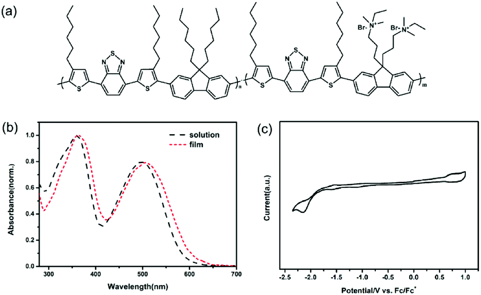 | ||
| Fig. 1 (a) Chemical structure of the conjugated polyelectrolyte PFBTBr. (b) UV-vis spectra of PFBTBr in solution and PFBTBr film. (c) CV curves of PFBTBr. | ||
As determined by Gel permeation chromatography (GPC), the weight average molecular weight (Mw) and the polydispersity index (Mw/Mn) of the corresponding neutral polymer of PFBTBr is 7.13 and 1.72, respectively. The molar ratio of the fluorene segments to the benzothiadiazole based segments is 1:1. Because the presence of the acceptor units, the absorption of PFBTBr is largely red-shifted to 700 nm compared with the polyfluorenes. As illustrated in Fig. 1b, PFBTBr in the diluted solution shows the strong UV-vis absorption from 300 to 700 nm, with two absorption peaks at 360 and 500 nm. While the absorption spectra of PFBTBr film is slightly red-shifted, corresponding to the π–π stacking of the backbones in the film. After annealed at 350 °C for 10 min, a further red-shift for the peak at 500 nm can be observed (Fig. S3†), which indicates that the thermal annealing leads to more orderly interchain face-to-face packing of the backbone rings. The red-shift absorption and the ordered stacking of PFBTBr are beneficial to the sunlight harvest and charge transport of the device.
In addition, the absorption spectrum of PFBTBr displays an absorption edge at 610 nm, corresponding to an optical band gap of 2.03 eV. The electrochemical cyclic voltammetry (CV) was performed to measure the molecular energy levels of PFBTBr by using the ferrocene/ferrocenium (Fc/Fc+) redox couple as the external standard. Based on the oxidation and reduction onset potentials shown in Fig. 1c, the HOMO and lowest unoccupied molecular orbital (LUMO) levels of PFBTBr are calculated to be −5.31 and −2.86 eV, respectively. UPS was also applied to investigate the HOMO levels of the PFBTBr film (Fig. S4†). By subtracting the onset of the low-binding-energy photoemission from the onset of the secondary electron energy cutoff and then subtracting the excitation photoenergy (21.2 eV), the HOMO level of PFBTBr is estimated to be −5.31 eV, which is in accordance with the result from the CV measurement. Therefore, PFBTBr possesses a relatively deep HOMO level compared with other reported green solvent soluble conjugated polymers, which could help to achieve larger Voc.
In the design of green solvent soluble conjugated polyelectrolytes, polymers with good solubility in green solvent is not only important to minimize the environmental impact for future industrialization, but also a key factor for the ease of material processability to achieve superior photovoltaic performance. For PFBTBr, alkylamine side chains were incorporated in the synthesis of the monomer 3. After polymerization, the neutral polymer was quaternarized to obtain a 40% quaternary ammonium group concentration, which guarantees the excellent solubility of PFBTBr in the green solvent DMF. Therefore, the extended absorption spectrum, appropriate energy levels and enhanced solubility imply that the conjugated polyelectrolyte PFBTBr is a promising donor material for HSCs.
Photovoltaic properties
Water soluble CdTe NCs were chosen as the acceptor material because of their high performance in the field of photovoltaic devices. The as-synthesized CdTe NCs are covered by mercaptoethylamine, which endow them superior water solubility and excellent film forming property. From the TEM measurement (Fig. S5a†), the as-prepared CdTe NCs are spherical with an average diameter of 2.97 nm. The CdTe NCs film also exhibits a UV-vis absorption spectrum range from 300 to 700 nm, with an absorption peak at 511 nm. After annealing, the absorption spectrum of CdTe NCs largely red-shifts to the near infrared region with the absorption peak at 824 nm (Fig. 2a), which can efficiently complement the absorption of PFBTBr. Since DMF is miscible with water, and the electrostatic repulsion between mercaptoethylamine ligands on the surface of CdTe NCs and the quaternary ammonium groups on the side chain of PFBTBr can prevent their aggregation with each other, the uniform blend between the conjugated polyelectrolyte and CdTe NCs can be realized. The annealed PFBTBr:CdTe blend film can cover a broad range of the sunlight spectrum with an enhanced absorption between 400 and 700 nm, proving the contribution of PFBTBr in the sunlight harvest (Fig. 2b).
 | ||
| Fig. 2 (a) UV-vis absorption spectra of the CdTe film with and without annealing. (b) UV-vis spectra of the CdTe film and PFBTBr:CdTe blend film. (c) Energy diagram and device structure of the PFBTBr:CdTe NCs based HSCs. (d) PL spectra of PFBTBr and PFBTBr:CdTe NCs mixed solutions. | ||
Because of the properly matched energy levels and the complementary absorption coverage (300 to 900 nm) of PFBTBr and CdTe NCs, the green-solvent-processed HSCs were fabricated by using conjugated polyelectrolyte PFBTBr as donor and CdTe NCs as acceptor. All HSCs were fabricated based on the same inverted device architecture: ITO/TiO2/CdTe/PFBTBr:CdTe/molybdenum oxide (MoO3)/Au. The CdTe/PFBTBr:CdTe n–i structure, where n refers to the acceptor and i refers to the blend of donor and acceptor, was utilized to further increase the light absorption as well as the charge separation and extraction.33 When fabricating the active layer, PFBTBr and CdTe NCs were dissolved separately in DMF and water, and then mixed as the processing solution. To ensure the compatibility of PFBTBr and CdTe NCs, PL spectra of the PFBTBr and PFBTBr:CdTe mixed solution are measured and summarized in Fig. 2d. The fluorescence of PFBTBr is significantly quenched after mixing with CdTe NCs, implying an efficient charge transfer between PFBTBr and CdTe NCs.
The device performance of the HSCs was investigated by measuring the current density versus voltage (J–V) curves of the devices under a simulated AM 1.5 spectrum. The D/A ratio are crucial for the internal build-in voltage and balance of photoinduced charge transfer and transport. The photovoltaic performance of devices with different PFBTBr:CdTe weight ratio were measured. As shown in Fig. 3a and Table S1,† when the PFBTBr:CdTe weight ratio is 1:5, the CdTe NCs may be isolated by the surrounding conjugated polyelectrolyte, which strongly hinder the formation of electron pathway, inducing the low short circuit current (Jsc) and fill factor (FF). When CdTe is excessive (PFBTBr:CdTe = 1:40), the amount of conjugated polyelectrolyte is too small to provide the hole transport pathway, which largely decrease the Voc and Jsc. When the PFBTBr:CdTe weight ratio are 1:10, the highest Voc of 0.61 V and power conversion efficiency (PCE) of 2.96% are reached. Therefore, the PFBTBr:CdTe weight ratio of 1:10 are the optimized condition and were applied in the following device fabrication. In the fabrication process, the active layer was formed by spin-coating the PFBTBr:CdTe solution on the underlying layer at 700 rpm for 1 min. To increase the thickness of the active layer, PFBTBr:CdTe solution with four gradually increased concentrations were used (Fig. 3b and Table S2†). When the solution concentration is 73.3 mg mL−1 corresponding to the thickness of 85 nm, the best efficiency of 3.3% with Voc of 0.59 V, Jsc of 15.1 mA cm−2, and FF of 36.8% is achieved. As the concentration gradually increased, the PCE decreased, which should be attributed to the presence of agglomerates in the active layer.
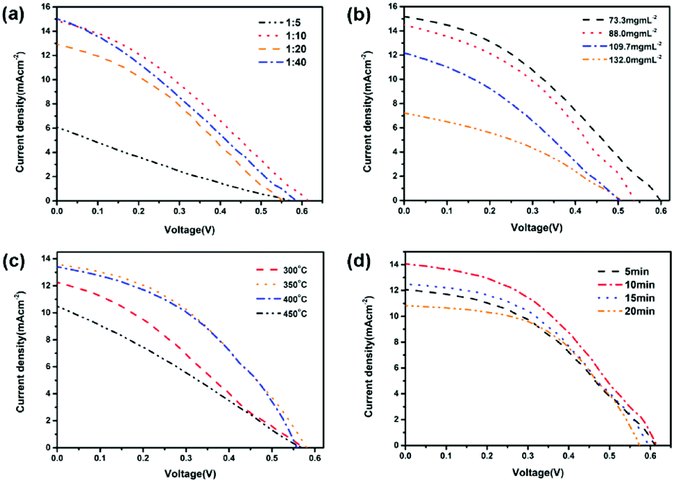 | ||
| Fig. 3 J–V curves of the PFBTBr:CdTe NCs based HSCs with different (a) D/A ratio (b) active layer solution concentration (c) annealing temperature of the active layer (d) annealing time of the active layer. | ||
Since the conjugated polyelectrolyte PFBTBr does not require the thermal annealing process, the device fabrication involving thermal annealing was performed to promote the removal of ligands and growth of the CdTe NCs. Upon annealing at different temperature, a PCE of 3.16% with Voc of 0.58 V, Jsc of 13.52 mA cm−2, FF of 40.39% was recorded under annealing at 350 °C for 5 min (Fig. 3c and Table S3†). The temperature of 350 °C ensured the elimination of the ligands as well as the growth of the CdTe NCs, which facilitated the light harvest and charge transport in the device. The dependence of the PCE on the annealing time was also investigated by varying the annealing time from 5 to 20 min (Fig. 3d and Table S4†). When the active layer was annealed for 10 min, PCE of 3.67% was reached with Voc of 0.62 V, Jsc of 13.99 mA cm−2, and FF of 42.45%. Therefore, the optimum performance was obtained through annealing the active layer at 350 °C for 10 min (Table 1).
:CdTe NCs based HSCs
| Voc (V) | Jsc (mA cm−2) | FF (%) | PCE (%) | |
|---|---|---|---|---|
| Basic | 0.62 | 13.99 | 42.45 | 3.67 |
| Optimized | 0.64 | 20.09 | 39.17 | 5.03 |
Morphology study
The morphology of the optimized PFBTBr:CdTe active layer was investigated by the AFM and TEM. The AFM phase images in tapping mode are usually utilized for distinguishing the interphase and revealing the material property differences in several systems.34–36 As shown in Fig. 4a and c, the CdTe film shows a brighter and uniform phase image, while the PFBTBr:CdTe blend film exhibits darker and larger domains belonging to the conjugated polyelectrolyte covered CdTe NCs phase, which strongly indicate the well mixing between CdTe NCs and PFBTBr. The AFM topography images also demonstrate that the PFBTBr:CdTe blend film is smoother with the RMS of 1.756 nm than the CdTe film (3.627 nm), owing to the existence of the conjugated polyelectrolyte PFBTBr (Fig. 4b and d). The TEM image of the active layer in Fig. S5b† demonstrates that PFBTBr and CdTe NCs uniformly distribute in the film with similar domain size about 10 nm, which will facilitate the formation of continuous electron/hole pathway and efficient charge transport.
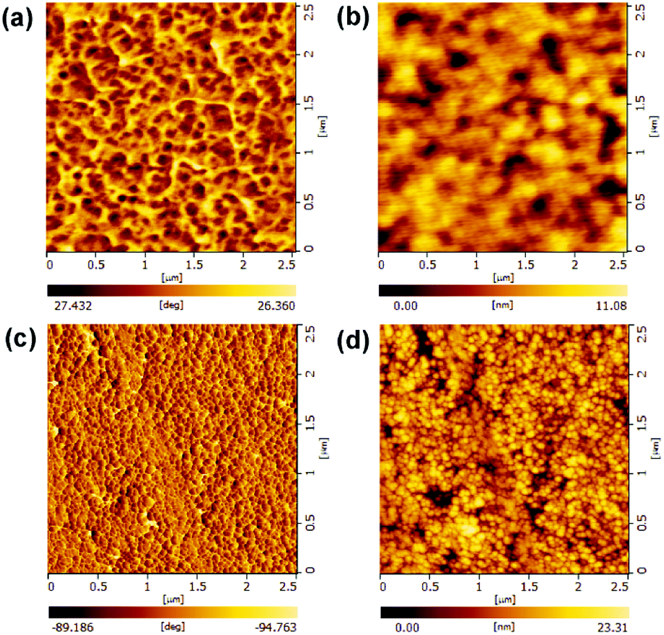 | ||
| Fig. 4 Atomic force microscopy images of the (a and b) PFBTBr:CdTe film and (c and d) CdTe film: phase (left) and topography (right) images. | ||
Device optimization
Further device optimization was performed to improve the photovoltaic performance of the PFBTBr:CdTe based HSCs. As well known, the interfacial engineering of the HSCs is crucial for the efficient charge separation and transport at the interface of the device. In this case, the MoO3 was selected as the hole transport layer material. Due to the insulating nature of MoO3, the device performance is sensitive to the thickness of the MoO3 layer. Therefore, the influence of the MoO3 layer thickness on the device performance was investigated (Fig. 5a and Table S5†). When the thickness of the MoO3 layer is 1.5 nm, the PCE is significantly improved to 4.49%, with Voc of 0.62 V, Jsc of 16.34 mA cm−2, FF of 44.29%.
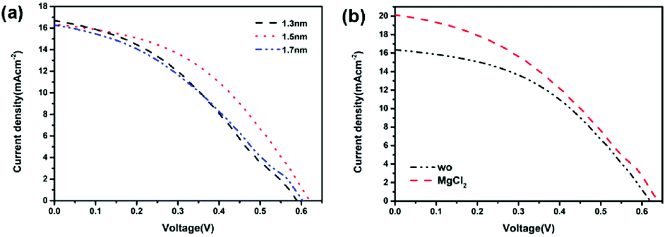 | ||
| Fig. 5 J–V curves of the PFBTBr:CdTe NCs based HSCs with (a) different MoO3 thicknesses, (b) MgCl2 treatment. | ||
It has been reported that the chloride treatment is an essential manufacturing process in the CdTe thin film solar cells to achieve high device efficiencies by passivating the grain boundaries, triggering the recrystallization and p-type doping passivation of the CdTe film etc.37–40 Therefore, the chloride treatment was introduced to investigate the influence of chloride treatment on the device performance of PFBTBr:CdTe based HSCs (Fig. 5b and Table S6†). Herein, the chloride treatment was performed by spin-coating the saturated MgCl2 methanol solution at 700 rpm on the top of the CdTe layer. After the chloride treatment, the Voc and Jsc of the devices largely increase from 0.62 to 0.64 V, 16.34 to 20.09 mA cm−2, respectively. Therefore, the maximum PCE of 5.03% is achieved for the PFBTBr:CdTe based HSCs (Table 1). The corresponding EQE curve shows that the device reaches its maximum EQE value of 87.01% at 400 nm (Fig. S6†).
Conclusions
In summary, a quaternary ammonium side chain modified conjugated polyelectrolyte PFBTBr was synthesized as the donor material for the green-solvent-processed HSCs. The incorporation of the quaternary ammonium groups ensures an excellent solubility of PFBTBr in the green solvent DMF. Moreover, by introducing the D–A strategy, PFBTBr shows a wide absorption from 300 to 700 nm and a relative deep HOMO level. To achieve the complementary sunlight harvest and properly matched energy level, the high efficient water soluble CdTe NCs were chosen and prepared as the acceptor material. By processing with the non-aromatic and halogen-free solvents DMF and water, the HSCs based on the conjugated polyelectrolyte PFBTBr and CdTe NCs were fabricated. Upon the optimum D/A ratio (1:10), active layer thickness (85 nm) and annealing condition (350 °C for 10 min), a PCE of 3.67% was obtained. With the active layer optimization, a desirable morphology of the active layer was observed by the AFM and TEM, which exhibits homogeneous D/A distribution, continuous electron/hole transport pathway and smoother surface. To further improve the performance of the HSCs, the anode interfacial modification and chloride treatment were introduced in the device optimization. And the PCE of the HSCs is enhanced to 5.03% with the maximum EQE value of 87.01% at 400 nm. Overall, the introduction of the conjugated polyelectrolyte could not only enable the green-solvent-processed device fabrication procedure, but also realize the improvement of the photovoltaic performance through the rational design of the molecular, which shows a bright future for the high-efficiency green-solvent-processed HSCs.
Experimental
Chemicals
Tellurium powder (200 mesh, 99.8%), cadmium chloride hemipentahydrate (99%) and sodium borohydride (99%) were obtained from Sinopharm Chemical Reagent Co. Ltd. 2-Mercaptoethylamine (MA; 98%), molybdenum oxide (>99%), tetrabutyl titanate (98%), sodium hydroxide (99%) and hydrochloric acid (36–38%) were obtained from Acros. All materials and solvents were used as received.Synthesis of the conjugated polyelectrolyte
5 mg of Pd(PPh3)4 and several drops of Aliquat 336 were dissolved in a mixture of toluene (6 mL) and Na2CO3 aqueous solution (2 M, 2 mL). Then 0.5 mmol M1, 2 and 3 with the ratio of 10:2:8 were added. The mixture was refluxed at 92 °C for 72 h under the nitrogen atmosphere. After cooling to room temperature, the mixture was poured into the methanol/water (10:1) solution and froze for 48 h. The obtained material was filtrated through a funnel. Then the oligomers and catalyst residues were removed by washing the obtained solid material for 12 h. After that, the neutral polymer was obtained by using chloroform and named PFBT. Following, 100 mg PFBT was dissolved in the mixture of DMSO (10 mL), bromoethane (2 mL) and THF (40 mL) and stirred at 50 °C for 120 h. Then the THF and bromoethane were evaporated, and 80 mL of ethyl acetate was added. The polymer was precipitated and collected by centrifugation. After washed with chloroform and THF, the material was dried overnight at 80 °C under vacuum. The obtained polyelectrolyte was named PFBTBr. 1H NMR (500 MHz, CDCl3, TMS): δ (ppm) 8.11–8.07 (m, Ar–H), 7.92–7.88 (m, Ar–H), 7.56–7.52 (m, Ar–H), 2.83–2.63 (m, Ar–CH2–), 2.00–1.98 (m, –(CH2)n–), 1.41–1.33 (m, –(CH2)n–), 0.91–0.79 (m, –CH3).
Synthesis of aqueous CdTe NCs
Aqueous CdTe precursors were obtained by injecting 0.28 mL NaHTe solution (1 M) to 70 mL N2 saturated MA and CdCl2 (12.5 mM) mixed solution at the pH range from 5.7–5.74, with a molar ratio of Cd2+/MPA/HSe− 1:1.5:0.2. Then, the mixed solution was refluxed at 100 °C for 60 min. After that, the CdTe NCs were obtained by centrifuging at 6000 rpm for 5 min in the presence of isopropanol. After drying in a vacuum oven at room temperature, the obtained CdTe NCs solid was weighed and dissolved in certain amount of deionized water to get CdTe NCs solution with desire concentration.
Device fabrication
The indium tin oxide (ITO) glasses were washed by sonicating in ethanol, acetone, isopropyl alcohol in turn. Then the O2 plasma was performed on ITO for 10 min. The electron transport layer TiO2 was obtained by spincoating the tetrabutyltitanate solution on the ITO glass with a speed of 2000 rpm and then annealed at 350 °C for 15 min. The CdTe NCs solution was then dropped onto the TiO2 layer and spin-coated at 700 rpm for 40 s in the air. The CdTe layer went through an annealing process in N2 at 350 °C for 2 min. Then, the PFBTBr:CdTe NCs mixture solution was spin-coated at 700 rpm for 40 s and annealed at 350 °C for 10 min in N2. The chloride treatment was applied by spincoating the chloride saturated methanol solution onto the CdTe layer and annealed in N2 at 350 °C for 2 min. Finally, the hole transport layer MoO3 (1.5 nm) and anode Au (80 nm) were vacuum evaporated on the active layer at a pressure below 10−5 torr, with a 5 mm2 active area.
Characterization
Gel permeation chromatography (GPC) analysis was carried out with a Waters 410 instrument using tetrahydrofuran as the eluent flow rate of 1 mL min−1, at 35 °C and polystyrene as the standard. 1H NMR and 13C NMR spectra were measured using a Bruker AVANCE-500 NMR spectrometer and a Varian Mercury-300 NMR, respectively. UV-vis absorption spectra were measured by a Lambda 800 UV-vis spectrophotometer. A a JEM-2100F electron microscope was used to conduct TEM. The Bruker Dimension Icon was used to perform the AFM measurements. An integrated ultrahigh-vacuum system equipped with a multitechnique surface analysis system (VG Scienta R3000) for ultraviolet photoelectron spectroscopy (UPS) was used to obtain the energy band values. The electrochemical cyclic voltammetry (CV) was conducted on a Bioanalytical Systems BAS 100 B/W electrochemical workstation. The photoluminescence (PL) spectra were implemented with a Shimadzu RF-5301 PC spectrophotometer. Under the AM 1.5 G 100 mW cm−2 illumination, a computer-controlled Keithley 2400 sourcemeter system was used to measure the current density versus voltage (J–V) characteristics. A Crowntech QTest Station 1000AD was used to measure the external quantum efficiency (EQE).Conflicts of interest
There are no conflicts to declare.Acknowledgements
This work was supported by National Natural Science Foundation of China (No. 51803070, No. 21875086), the China Postdoctoral Science Foundation (Grant No. 2017M611312), the National Key Research and Development Program of China (No. 2016YFB0401701), JLU Science and Technology Innovative Research Team (2017TD-06) and the Special Project from MOST of China.References
- A. J. Maclachlan, T. Rath, U. B. Cappel, S. A. Dowland, H. Amenitsch, A. Knall, C. Buchmaier, G. Trimmel, J. Nelson and S. A. Haque, Adv. Funct. Mater., 2015, 25, 409–420 CrossRef CAS PubMed.
- L. Whittaker-Brooks, J. Gao, A. K. Hailey, C. R. Thomas, N. Yao and Y. Loo, J. Mater. Chem. C, 2015, 3, 2686–2692 RSC.
- J. Yuan, A. Gallagher, Z. Liu, Y. Sun and W. Ma, J. Mater. Chem. A, 2015, 3, 2572–2579 RSC.
- Y. Sun, Z. Liu, J. Yuan, J. Chen, Y. Zhou, X. Huang and W. Ma, Org. Electron., 2015, 24, 263–271 CrossRef CAS.
- E. Zimmermann, T. Pfadler, J. Kalb, J. A. Dorman, D. Sommer, G. Hahn, J. Weickert and L. Schmidt-Mende, Adv. Sci., 2015, 2, 1500059 CrossRef PubMed.
- C. Giansante, R. Mastria, G. Lerario, L. Moretti, I. Kriegel, F. Scotognella, G. Lanzani, S. Carallo, M. Esposito, M. Biasiucci, A. Rizzo and G. Gigli, Adv. Funct. Mater., 2015, 25, 111–119 CrossRef CAS.
- J. P. Thomas, S. Srivastava, L. Zhao, M. Abd-Ellah, D. McGillivray, J. S. Kang, M. A. Rahman, N. Moghimi, N. F. Heinig and K. T. Leung, ACS Appl. Mater. Interfaces, 2015, 7, 7466–7470 CrossRef CAS PubMed.
- H. Lu, J. Joy, R. L. Gasper, S. E. Bradforth and R. L. Brutchey, Chem. Mater., 2016, 28, 1897–1906 CrossRef CAS.
- A. Lefrancois, B. Luszczynska, B. Pepin-Donat, C. Lombard, B. Bouthinon, J. Verilhac, M. Gromova, J. Faure-Vincent, S. Pouget, F. Chandezon, S. Sadki and P. Reiss, Sci. Rep., 2015, 5, 7768 CrossRef CAS PubMed.
- R. Mastria, A. Rizzo, C. Giansante, D. Ballarini, L. Dominici, O. Inganas and G. Gigli, J. Phys. Chem. C, 2015, 119, 14972–14979 CrossRef CAS.
- W. Guo, J. Yuan, H. Yuan, F. Jin, L. Han, C. Sheng, W. Ma and H. Zhao, Adv. Funct. Mater., 2016, 26, 713–721 CrossRef CAS.
- F. S. F. Morgenstern, M. L. Bohm, R. J. P. Kist, A. Sadhanala, S. Gelinas, A. Rao and N. C. Greenham, J. Phys. Chem. C, 2016, 120, 19064–19069 CrossRef CAS.
- Q. Zeng, X. Zhang, X. Feng, S. Lu, Z. Chen, X. Yong, S. Redfern, H. Wei, H. Wang, H. Shen, W. Zhang, W. Zheng, H. Zhang, J. Tse and B. Yang, Adv. Mater., 2018, 30, 1705393 CrossRef PubMed.
- Q. Qiao, L. Su, J. Beck and J. T. McLeskey, J. Appl. Phys., 2005, 98, 094906 CrossRef.
- W. Yu, H. Zhang, Z. Fan, J. Zhang, H. Wei, D. Zhou, B. Xu, F. Li, W. Tian and B. Yang, Energy Environ. Sci., 2011, 4, 2831–2834 RSC.
- G. Jin, N. Chen, Q. Zeng, F. Liu, W. Yuan, S. Xiang, T. Feng, X. Du, T. Ji, L. Wang, H. Sun, H. Sun and B. Yang, Adv. Energy Mater., 2018, 8, 1701966 CrossRef.
- Z. Chen, X. Du, Q. Zeng and B. Yang, Mater. Chem. Front., 2017, 1, 1502–1513 RSC.
- X. Du, Q. Zeng, G. Jin, F. Liu, T. Ji, Y. Yue, Y. Yang, H. Zhang and B. Yang, Small, 2017, 13, 1603771 CrossRef PubMed.
- Q. Zeng, Z. Chen, F. Liu, G. Jin, X. Du, T. Ji, Y. Zhao, Y. Yue, H. Wang, D. Meng, T. Xie, H. Zhang and B. Yang, Sol. RRL, 2017, 1, 1600020 CrossRef.
- Z. Chen, H. Zhang, W. Yu, Z. Li, J. Hou, H. Wei, X. Du and B. Yang, Adv. Energy Mater., 2013, 3, 433–437 CrossRef CAS.
- S. Yao, Z. Chen, F. Li, B. Xu, J. Song, L. Yan, G. Jin, S. Wen, C. Wang, B. Yang and W. Tian, ACS Appl. Mater. Interfaces, 2015, 7, 7146–7152 CrossRef CAS PubMed.
- J. Li, Y. Li, J. Xu and C. K. Luscombe, ACS Appl. Mater. Interfaces, 2017, 9, 17942–17948 CrossRef CAS PubMed.
- S. Oh, S. Na, J. Jo, B. Lim, D. Vak and D. Kim, Adv. Funct. Mater., 2010, 20, 1977–1983 CrossRef CAS.
- T. Yang, M. Wang, C. Duan, X. Hu, L. Huang, J. Peng, F. Huang and X. Gong, Energy Environ. Sci., 2012, 5, 8208–8214 RSC.
- E. E. Havinga, W. T. Hoeve and H. Wynberg, Synth. Met., 1993, 55, 299–306 CrossRef CAS.
- H. Zhou, L. Yang, S. Stoneking and W. You, ACS Appl. Mater. Interfaces, 2010, 2, 1377–1383 CrossRef CAS PubMed.
- H. Zhou, L. Yang and W. You, Macromolecules, 2012, 45, 607–632 CrossRef CAS.
- G. K. V. V. Thalluri, J. Bolsee, A. Gadisa, M. Parchine, T. Boonen, J. D'Haen, A. E. Boyukbayram, J. Vandenbergh, T. J. Cleij, L. Lutsen, D. Vanderzande and J. Manca, Sol. Energy Mater. Sol. Cells, 2011, 95, 3262–3268 CrossRef CAS.
- X. Wang, E. Perzon, F. Oswald, F. Langa, S. Admassie, M. R. Andersson and O. Inganas, Adv. Funct. Mater., 2005, 15, 1665–1670 CrossRef CAS.
- M. Chen, J. Hou, Z. Hong, G. Yang, S. Sista, L. Chen and Y. Yang, Adv. Mater., 2009, 21, 4238–4242 CrossRef CAS.
- M. Bernius, M. Inbasekaran, E. Woo, W. Wu and L. J. Wujkowski, J. Mater. Sci.: Mater. Electron., 2000, 11, 111–116 CrossRef CAS.
- M. Svensson, F. Zhang, S. C. Veenstra, W. J. H. Verhees, J. Hummelen, J. M. Kroon and O. Inganas, Adv. Mater., 2003, 15, 988–991 CrossRef CAS.
- M. Hiramoto, H. Fujiwara and M. Yokoyama, Appl. Phys. Lett., 1991, 58, 1062–1064 CrossRef CAS.
- X. Zhang, B. Sun and R. H. Friend, Nano Lett., 2006, 6, 651–655 CrossRef CAS PubMed.
- I. Schmitz, M. Schreiner, G. Friedbacher and M. Grasserbauer, Appl. Surf. Sci., 1997, 115, 190–198 CrossRef CAS.
- Z. Guo, T. Pereira, O. Choi, Y. Wang and H. T. Hahn, J. Mater. Chem., 2006, 16, 2800–2808 RSC.
- J. D. Major, R. E. Treharne, L. J. Phillips and K. Durose, Nature, 2014, 511, 334–337 CrossRef CAS PubMed.
- J. D. Major, M. A. Turkestani, L. Bowen, M. Brossard, C. Li, P. Lagoudakis, S. J. Pennycook, L. J. Phillips, R. E. Treharne and K. Durose, Nat. Commun., 2016, 7, 13231 CrossRef CAS PubMed.
- B. Ghosh, D. Ghosh, S. Hussain, G. Amarendra, B. R. Chakraborty, M. K. Dalai, G. Sehgal, R. Bhar and A. K. Pal, Mater. Sci. Semicond. Process., 2014, 24, 74–82 CrossRef CAS.
- Y. F. Yan, M. M. Al-Jassim and K. M. Jones, J. Appl. Phys., 2004, 96, 320–326 CrossRef CAS.
Footnote |
| † Electronic supplementary information (ESI) available. See DOI: 10.1039/c8ra07884j |
| This journal is © The Royal Society of Chemistry 2018 |