
 Open Access Article
 This Open Access Article is licensed under a Creative Commons Attribution-Non Commercial 3.0 Unported Licence
Hydrogenated derivatives of hexacoordinated metallic Cu2Si monolayer†‡
E. Unsal *a,
F. Iyikanata,
H. Sahinbc and
R. T. Sengerac
*a,
F. Iyikanata,
H. Sahinbc and
R. T. Sengerac
aDepartment of Physics, Izmir Institute of Technology, 35430, Izmir, Turkey. E-mail: elifunsal@iyte.edu.tr
bDepartment of Photonics, Izmir Institute of Technology, 35430, Izmir, Turkey
cICTP-ECAR Eurasian Center for Advanced Research, Izmir Institute of Technology, 35430, Izmir, Turkey
First published on 30th November 2018
Abstract
Herein, we carried out first-principles calculations based on density functional theory to investigate the effects of surface functionalization with hydrogen atoms on structural, dynamical and electronic properties of Cu2Si monolayer. Pristine Cu2Si, a metallic monolayer, has a planar hexacoordinate structure. Calculations revealed that the most favorable position of a single H atom on the Cu2Si monolayer is at the top of a Si site. Derivatives of Cu2Si monolayer with various H concentrations were investigated, and by performing phonon calculations, it was found that there are three stable hydrogenated structures. Specific heat of these monolayers was found to increase with the hydrogen concentration at temperatures higher than 100 K. Electronically, the hydrogenated derivatives of Cu2Si monolayer preserve the metallic character.
I. Introduction
Following the successful isolation of graphene,1 the family of two-dimensional (2D) materials has attracted great attention. This family has a large variety of members including mono-atomic honeycomb structures (silicene,2 germanene3), transition metal dichalcogenides (MoS2,4 WS2,5 ReS2 (ref. 6)) and group III–V compounds (h-BN,7 h-AlN8,9). Recently, Yang et al. proposed a new class of highly stable planar hypercoordinated materials, such as hexacoordinated Ni2Ge,10 Cu2Ge,11 Cu2As,12 Au13 and Cu,14 which open up a new branch for the 2D materials. Those materials have attracted attention due to their structural and mechanical properties such as strong chemical bonding and in-plane stiffness.One of these novel materials is the monolayer Cu2Si15 with planar hexacoordinated Cu and Si motifs. It is a nonmagnetic metal with high stability stemming from the superposition of 4c–2e σ bonds extended within the 2D sheet. The metallicity of Cu2Si has been known, Feng et al. verified Dirac nodal line fermions in Cu2Si monolayer by using angle-resolved photoemission spectroscopy and first-principles calculations.16 Nodal line semimetals,17,18 a type of topological semimetals, have symmetry-protected linear-band crossing points near the Fermi level and they have been intensively studied previously.19 These materials are suitable candidates for the realization of high-speed, low-dissipation devices.16
Chemical functionalization of 2D materials is one of the most common methods to tune the structural,20 electronic21 and magnetic22 properties of a material. For instance, H and F atoms are commonly used for the surface functionalization of the 2D materials. Following the theoretical prediction of hydrogenated graphene (graphene),23 Elias et al. achieved the synthesis of the graphene and showed that the reversible hydrogenation process changes graphene into an insulator.24 Moreover, Nair et al. achieved to synthesize fluorinated graphene (fluorographene) which possesses completely different electronic properties than that of graphene.25 Although graphene is a highly conductive semimetal, fluorographene is an insulator with an optical gap of 3 eV. Recently, we reported that when the charge density wave (CDW) phase of single-layer TiSe2 is fully hydrogenated, the structure transforms to a distorted T-phase (Td).26 In the mean time, hydrogenation is also used for the passivation of interfaces and contacts.27,28 For instance, electrical conductivity of metals can be changed through various manipulations such as binding foreign molecules or adatoms.29 During experiments, the presence of the environmental interactions is inevitable; therefore, the passivation of such materials plays important role in achieving a stable electrical behavior. When the material is hydrogenated, the hydrogen layer acts as a protective layer against the external influences while preserving the electronic properties of the structure.
Even though there are several analyses on structural, chemical and electronic properties of the Cu2Si, the effect of hydrogenation has not been studied thoroughly. Herein, we present an investigation of the feasibility of the hydrogenation of the Cu2Si monolayer based on density-functional theory. Starting from single atom adsorption, structural, electronic and vibrational properties of Cu2Si covered with various concentrations of hydrogen are investigated. Three possible structures of hydrogenated Cu2Si are found to be dynamically stable. As well as the pristine structure, hydrogenated derivatives of Cu2Si monolayer exhibit metallic behavior. Moreover, it is found that the hydrogenation of Cu2Si monolayer leads to an increase in its specific heat at temperatures higher than 100 K and it reduces the surface activity of the material against other foreign agents without effecting its metallic character and planar geometry.
The paper is organized as follows: detailed information about computational methodology is given in Sec. II. The structural, vibrational and electronic properties of pristine Cu2Si, and also the adsorption and diffusion of a hydrogen atom on Cu2Si are discussed in Sec. III. In Sec. IV, we present the structural, vibrational and electronic properties of the hydrogenated derivatives of Cu2Si monolayer. Lastly, Sec. V is allocated for the conclusions.
II. Computational methods
In order to investigate surface functionalization of Cu2Si monolayer, density functional theory (DFT)-based calculations were performed by using the Vienna ab initio Simulation Package (VASP).30,31 In order to describe the exchange and correlation energies, Perdew–Burke–Ernzerhof (PBE) form of the generalized gradient approximation (GGA) functional was adopted.32 DFT-D2 method of Grimme was used for the van der Waals (vdW) correction to the GGA functional.33 Bader technique was used in order to determine the charge transfers in the structure.35,36Energy cutoff of the plane-wave basis set was chosen to be 500 eV. For the convergence criterion, the energy difference between successive electronic steps was taken to be 10−5 eV and the Hellmann–Feynman forces on each atom were reduced to a value of less than 10−4 eV Å−1. A vacuum space of 12 Å was incorporated in order to avoid the interactions between the adjacent layers. 18 × 18 × 1 Γ-centered mesh was used for the Brillouin Zone (BZ) integration of the unit cell and the mesh is scaled accordingly for larger supercells.
Cohesive energy per atom (Ecoh) was calculated for each structure, by using the following formula,
 | (1) |
III. Adsorption and diffusion of hydrogen on Cu2Si
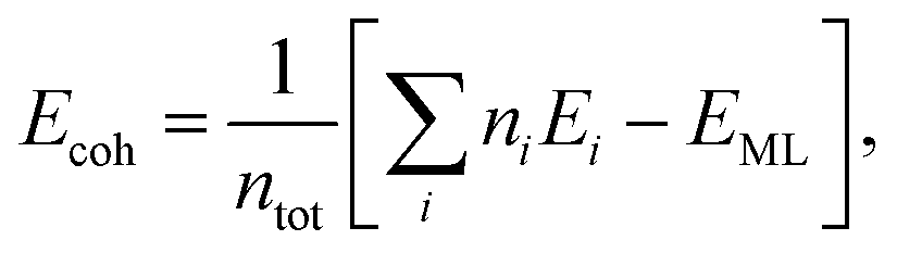
Cu2Si monolayer has a planar structure that consists of a hexagonal sublattice of Cu atoms and a trigonal sublattice of Si atoms. The primitive unit cell of the structure includes two Cu atoms and one Si atom as seen from its optimized structure shown in Fig. 1(a). The calculated structural parameters are given in Table 1. It is found that the lattice constant of the Cu2Si monolayer is 4.10 Å each Cu coordinates with three Si and three Cu atoms while each Si coordinates only with six Cu atoms. It is calculated that Cu–Si and Cu–Cu bond lengths are equal and 2.37 Å. Lattice parameter and bond length calculations are consistent with the values reported by Yang et al. (a = b = 4.123 Å, dCu–Si = dCu–Cu = 2.38 Å).15 According to Bader charge analysis, each Si atom donates 0.2e to Cu atoms indicating the covalent character of Cu–Si bonds.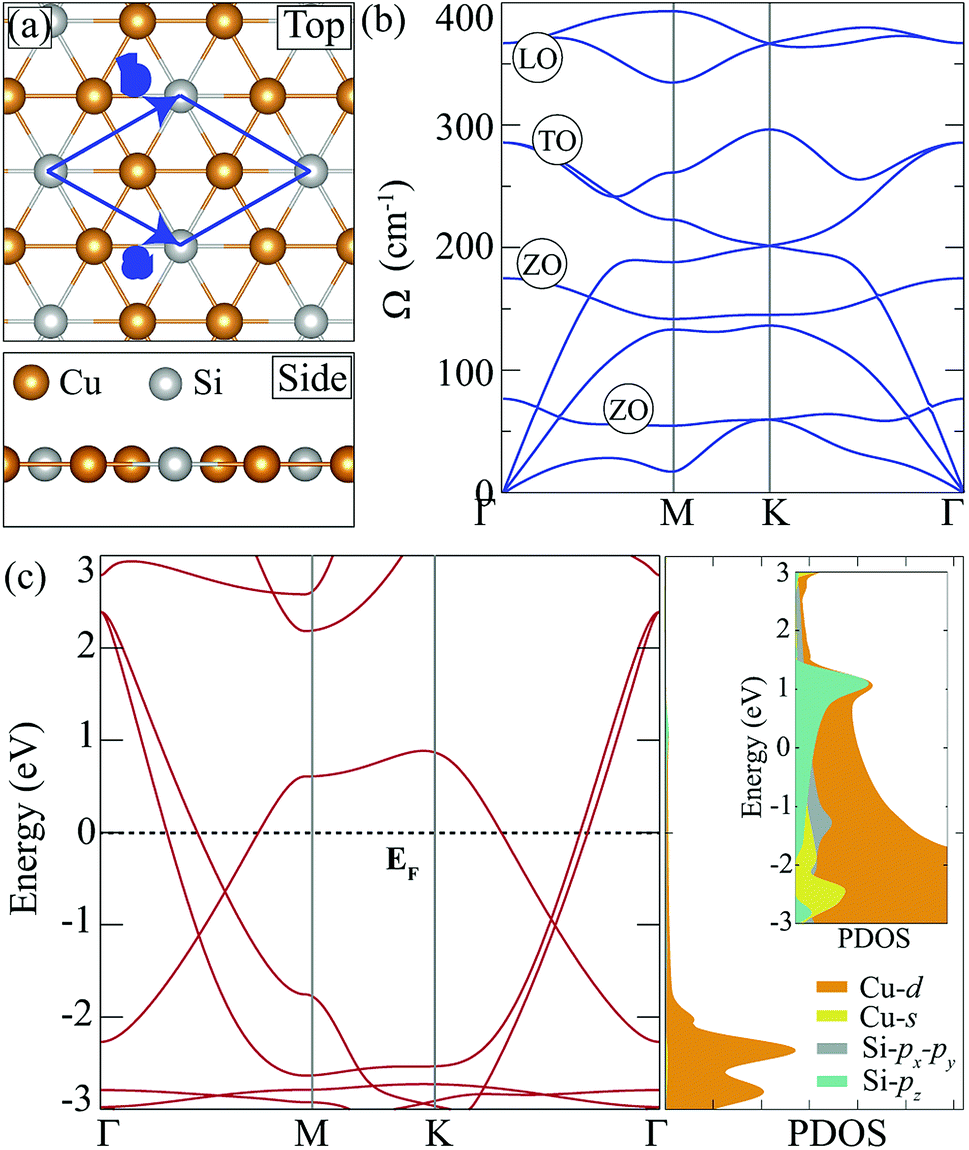 | ||
| Fig. 1 (a) Top and side views of the pristine Cu2Si monolayer. The blue rhombus represents the unit cell. (b) The phonon band dispersion of 5 × 5 × 1 supercell of Cu2Si monolayer is displayed through the irreducible Brillouin zone. (c) The electronic band dispersion and partial density of states (PDOS) for the primitive unit cell of Cu2Si monolayer. Fermi level (EF) is set to zero. | ||
| a (Å) | b (Å) | γ (°) | dCu–Si (Å) | dCu–Cu (Å) | Δρ (e) | Ecoh (eV per atom) | |
|---|---|---|---|---|---|---|---|
| Cu2Si | 4.10 | 4.10 | 60.0 | 2.37 | 2.37 | 0.2 | 3.55 |
| LowH-d | 8.09 | 8.09 | 58.4 | 2.33–2.44 | 2.34–2.46 | 0.4 | 3.57 |
| HighH-s | 4.12 | 4.12 | 60.0 | 2.41 | 2.38 | 0.6 | 3.59 |
| HighH-d | 8.21 | 8.27 | 59.7 | 2.41–2.42 | 2.38 | 0.6 | 3.59 |
In order to investigate dynamical stability, phonon band dispersion of the Cu2Si monolayer is calculated and is shown in Fig. 1(b). A 5 × 5 × 1 supercell is used for the phonon band structure calculations and it is found that the Cu2Si monolayer is dynamically stable. As seen in the figure, the signature of a Kohn-type soft phonon mode appears at the M point in the BZ.38 The highest-frequency modes, longitudinal optical (LO) modes, are mainly composed of the in-plane motions of Si atoms. The transverse optical (TO) modes that represent the out of phase vibrations of Cu atoms, have lower frequencies than that of the LO modes. Fig. 1(b) shows that Cu2Si monolayer has 2 optical flexural (ZO) modes. While the low-frequency mode is composed of out-of-plane motions of Cu atoms in opposite direction, the other mode consists of counter-phase motions of Cu and Si atoms in the out-of-plane direction. Compared to the typical 2D materials such as graphene (∼1500 cm−1),39 h-BN (∼1600 cm−1)40 and MoS2 (∼480 cm−1),41 phonon modes of the Cu2Si monolayer reside at lower energies.
Fig. 1(c) illustrates the electronic band dispersion and the partial density of states (PDOS) of the Cu2Si monolayer. As can be seen in the figure, the Cu2Si monolayer is a metal and exhibits nodal lines around the Γ point. Extensive discussion of nodal loops in Cu2Si monolayer can be found in a previous study by Feng et al.16 Moreover PDOS of Cu2Si monolayer reveals that the major contribution to the states around the Fermi level originates from Cu-d and Si-p orbitals. Analysis on the various ground state magnetic orders reveals that the ground state of the pristine monolayer of Cu2Si is nonmagnetic as previously reported by Yang et al.15
The investigation of adsorption of a single H atom on Cu2Si monolayer is essential for understanding the possible hydrogenation scenarios of the material. In order to simulate an isolated H adatom, the size of the supercell is chosen to be 3 × 3 × 1. While having the same electronegativity of 1.90 (in Pauling scale) provides isotropic Si–Si and Cu–Cu bonds, the difference in their electron affinities (Cu: 118.4 and Si: 133.6 kJ mol−1) causes a difference in their hydrogen adsorption process. It is expected that the Si atom provides a stronger attraction on H atom than the Cu atom. For the adsorption process of a single H atom, there are five different high-symmetry lattice sites: Si, Cu, hollow, bridge site between Cu and Si atoms (BCu–Si) and bridge site between the two Cu atoms (BCu–Cu) which are shown in Fig. 2(a). H atoms placed at the BCu–Cu and the Cu sites, settle at those sites with binding energies of −2.18 and −1.72 eV, respectively. However, when the H atom is located on the BCu–Su and the hollow sites, it moves towards Si site and settles. When a single H atom is placed directly on top of Si atom, it settles at this site with a binding energy of −2.80 eV. Therefore, Si is the most favorable lattice site for the H adatom with a calculated Si–H bond length of 1.51 Å. This value is close to the reported experimental Si–H bond length in silane (1.46 Å)42 and the calculated bond length from the summation of the covalent radii of Si and H atoms (rSi + rH = 1.42 Å). According to Bader charge analysis, Si atom transfers 0.6e charge to the H atom which gives a partial ionic character to the Si–H bond.
 | ||
| Fig. 2 (a) For a single H adatom, the energy variation between the high symmetry points of the hexagonal structure is demonstrated. The binding energy at Si site is set to zero. (b) Energy landscape for single H adatom adsorbed on Cu2Si monolayer. Blue and red colors represent the Si and Cu sites, respectively. EQ = 0.72 eV is the lowest energy barrier through the migration path shown with green dashed arrow. The energy values on the scale are in units of eV. (c) Folded electronic band structure of 3 × 3 × 1 Cu2Si monolayer in which single H adsorbed on Si site. Fermi level, EF, is set to zero. | ||
In order to find the migration path of H atom on Cu2Si monolayer, variation of its total energy on different lattice points is also analyzed. The energy barriers that the adsorbed H atom encounters are demonstrated in Fig. 2(a) and (b), respectively. For the calculation of the energy landscape, the position of the H adatom relative to the surface is fixed while its movement along the perpendicular direction is allowed. The paths considered are shown with black dashed lines in the inset of Fig. 2(a). The results show that the lowest energy barrier is 0.72 eV which occurs when the H atom moves from one Si site to another through the BCu–Cu. The migration path of Si–H–BCu–Cu–H–Si is presented with the green dashed arrow in Fig. 2(b). Diffusion over the Cu site has the highest energy barrier which is calculated to be 1.09 eV.
The contribution of a single H adatom to the electronic band structure of Cu2Si monolayer is also investigated. Folded electronic band dispersion of 3 × 3 × 1 monolayer of a single H atom adsorbed Cu2Si is shown in Fig. 2(c). It is seen that adsorbed H atom does not change the metallic character of Cu2Si monolayer. Moreover, the nonmagnetic ground state of the material is not affected by the adsorption of the H atom.
For the hydrogenation process, it is essential to understand the interaction between the H adatoms. We investigate 3 × 3 × 1 monolayer of Cu2Si in which two H adatoms are bonded to the Si sites from (i) one side (single-sided) and (ii) both sides (double-sided) of the monolayer. Since the separation of the two nearest Si sites is equal to 4.10 Å, the coupling between two H adatoms is negligible. The binding energies of single-sided and double-sided structures are calculated to be −2.68 and −2.66 eV, respectively. The bond strength between the Si and H atoms in the H-adsorbed Cu2Si is weaker than the one between two H atoms in the H2 molecule (−4.54 eV). Thus, for the hydrogenation of the pristine monolayer, an extra energy is required to dissociate the hydrogen atoms of the H2 molecule. In order to validate this discussion, adsorption of a H2 molecule on Cu2Si is also investigated and it is found that H2 molecule is physisorbed ∼4 Å above the pristine monolayer of Cu2Si with a weak vdW interaction of −0.20 eV. For this reason the hydrogenation of Cu2Si monolayer is only possible with the atomic hydrogen (which can be produced by hot wire chemical vapor deposition43,44). Feasibility of the hydrogenation is possible with the atomic hydrogen processes by doing plasma hydrogenation; in particular, plasma hydrogenation is used in synthesis of graphene.45
IV. Hydrogenated derivatives of Cu2Si
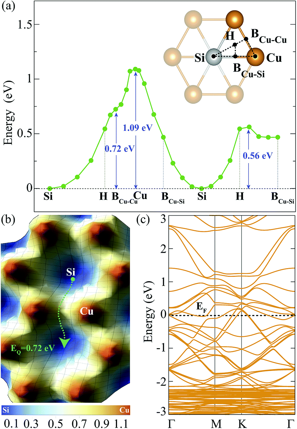
In this section, we investigate the structural, vibrational and electronic properties of hydrogenated derivatives of Cu2Si monolayer. We predict structures with various H coverage and analyze their stability by examining the vibrational spectra. Consistent with single atom adsorption calculations, surface coverage calculations show that H atoms do not prefer to bind on top of Cu atoms. It is found that the structures containing Cu–H bond are unable to generate the required restoring force against the atomic motions (see ref. 48). Here, we investigate three of the dynamically stable hydrogenated derivatives of Cu2Si monolayer with the highest hydrogen concentration. For convenience, we label these structures according to their percentage of hydrogen coverage and their hydrogenated surfaces. Structure with a stoichiometry of Cu4Si2H, which is hydrogenated from double sides and has a hydrogenation atomic ratio of 16.7%, is labeled as lowH-d. For other two structures, the hydrogen concentration is 33.3% and stoichiometry is Cu2SiH, but they differ in terms of the hydrogenated surfaces. Single-sided and double-sided Cu2SiH structures are labeled as highH-s and highH-d, respectively. Various other hydrogenation scenarios were also considered but they all led to instabilities in the vibrational spectra.A. Structural properties
Among the three hydrogenated derivatives, the monolayer lowH-d has the lowest amount of hydrogen. It has a unit cell containing 14 atoms and only the half of the Si atoms in the unit cell are hydrogenated. The hydrogenation leads to a 1.3% contraction of in-plane lattice constant of the Cu2Si monolayer. Although the a and b lattice parameters are found to be equal, its lattice structure is not a perfect hexagon since the angle between them is 58.4°. The bond lengths of Cu–Cu and Cu–Si are no longer equal to each other as is in the pristine structure and they vary from 2.33 to 2.46 Å. The bond distance between Si and H atoms is 1.51 Å. Bader charge analysis reveals that the average value of the total electron donation of each Si in lowH-d increases by 0.2e compared to the pristine monolayer.For the monolayers highH-s and highH-d, the H concentration is doubled. The monolayers of highH-s and highH-d contain 4 and 16 atoms in their unit cells, respectively. Compared to the pristine monolayer, the lattice constants for both of the structures are found to increase less than 1%. Although the monolayer of highH-s preserves its perfect hexagonal lattice structure, it is found that the monolayer of highH-d is slightly distorted. Calculated bond lengths of Si–H for the monolayers of highH-s and highH-d, are 1.51 Å and 1.52 Å, respectively. For highH-s and highH-d structures, the average electron donation of Si atom to H atom is calculated to be same with a value of 0.6e.
B. Vibrational properties
Here, we discuss how the vibrational properties of Cu2Si monolayer change with surface hydrogenation. The calculated phonon spectra of the hydrogenated derivatives of Cu2Si monolayer are demonstrated in Fig. 3(a)–(c). The vibrational analyses reveal that the monolayers of lowH-d, highH-s and highH-d have positive phonon branches through the whole BZ indicating the dynamical stability of the structures at T = 0 K. | ||
| Fig. 3 Top and side views, and phonon band structures of the hydrogenated monolayers: (a) lowH-d, (b) highH-s, and (c) highH-d. | ||
Since the unit cells of the pristine Cu2Si and highH-s are similar, their phonon band diagrams can be directly compared. Although there is a resemblance between their phonon band diagrams, LO and TO modes of pristine structure soften in the hydrogenated structure. Since Si atoms donate electron to the H atoms, the in-plane bonds of Si with Cu weaken and this leads to a decrease in the mode frequencies. On the other hand, ZO modes dominated by the Cu motions harden (which is discussed in Sec. IV C).
Furthermore, it is seen from the Fig. 3(a)–(c), the soft phonon mode previously seen at the M point of the phonon band diagram of Cu2Si monolayer disappears when the material is hydrogenated. Differing from the pristine Cu2Si, hydrogenated derivatives have high-frequency modes between 2000-2100 cm−1 (see Fig. 3) indicating the formation of strong Si–H bonds. H atoms are relatively much lighter than the Si and Cu atoms and thus, it is expected that the phonon modes that correspond to the Si–H bonds have much higher frequencies. These high-frequency modes have out-of plane character and include out-of-phase motions of Si and H atoms in all cases.
The effect of the hydrogenation on the constant-volume specific heat of the material is also investigated. The specific heat of structures as a function of phonon frequency, w, is calculated as follows,46
 | (2) |
Atom-projected partial phonon DOS of pristine and hydrogenated derivatives of Cu2Si monolayer are presented in Fig. 4(a). At the low frequencies (i.e. < 300 cm−1), it is seen that the main contribution to the DOS comes from the Cu atoms, whereas the DOS of Si atoms dominate at relatively high frequencies (from 300 to 430 cm−1) as expected from the masses of these atoms. In the highest frequency region (i.e. > 500 cm−1) contribution of the H atoms are dominant. The contribution of the Si atom in this region to the phonon DOS reveals the interaction of Si and H atoms.
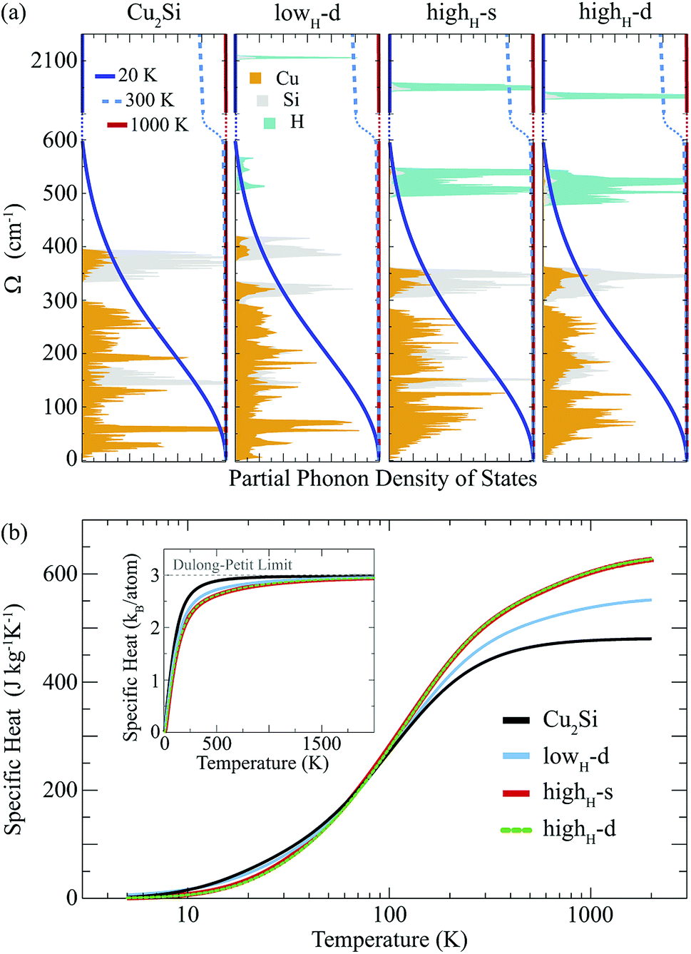 | ||
| Fig. 4 (a) Phonon partial density of states and derivative of the phonon occupation functions of the Cu2Si monolayer and its hydrogenated derivatives at various temperatures. Red, light and dark blue lines represent the functions calculated at 1000, 300, and 20 K. (b) For the Cu2Si monolayer and its hydrogenated derivatives, constant volume specific heat per mass is demonstrated as a function of temperature in logarithmic scale. | ||
Temperature dependent variation of the derivative of the phonon occupation functions are also illustrated in Fig. 4(a). These functions determine the contribution of vibrational modes to the specific heat of a material. It is evident that the hydrogen modes, which have very high frequency values, contribute more to the specific heat of the material at high temperatures. As a result of this, as the amount of hydrogenation increases, the higher temperature specific heat of the material also increases (see Fig. 4(b)). Moreover, it is well known that the hydrogenation of a material leads to decrease in its mass density which gives rise to an increase in its specific heat at high temperatures. As the temperature is lowered, the specific heat values of all these structures get close to each other, and at temperatures around 100 K, they merge to the same value. As the temperature is further lowered (around 20 K), the specific heat of pristine Cu2Si becomes higher than those of the hydrogenated derivatives. A similar crossover in the specific heat values is also reported for graphite and diamond structures.47 At room temperature specific heat values of Cu2Si, lowH-d, highH-s and highH-d are calculated to be 438, 470, 507 and 508 J kg−1 K−1, respectively. Moreover, in the inset of Fig. 4(b) the specific heat per atom of all the structures are also presented. As seen from the figure the pristine structure approaches the Dulong–Petit limit at much lower temperatures than the hydrogenated derivatives. Debye temperature values are calculated to be 429, 867, 1102, and 1078 K, for Cu2Si, lowH-d, highH-s and highH-d, respectively.
C. Electronic properties
Hydrogenation of a material is a common method to tune its electronic properties. It has been reported that while pristine graphene is a conductor, fully hydrogenated graphene is a semiconductor and half-hydrogenated graphene is a ferromagnetic, small band-gap material.24,37 In this section, hydrogen coverage dependency of the electronic structure of Cu2Si monolayer is investigated.As already mentioned in Sec. III, pristine Cu2Si is a metal and possesses nodal lines in its electronic structure. Electronic band dispersion and PDOS of hydrogenated derivatives of Cu2Si are shown in Fig. 5. For the sake of comparison, the band structure of the pristine Cu2Si is also added. As seen in the figure all of the hydrogenated derivatives preserve the metallic character as the pristine one. Although Cu2Si monolayer possesses robust metallic character against hydrogenation, some deviations appear in the electronic structure as the hydrogen concentration increases. It is clearly seen that while the two nodal lines of pristine Cu2Si reside between Γ and M points at 0.6 and 1.1 eV below the Fermi level, as the amount of hydrogen coverage increases, these nodal lines appear closer to the Fermi level (EF) and at higher energies for lowH-d and highH-d, respectively. As seen in Fig. 5 (b) and (c), an energy gap occurs between the nodal lines which reside between Γ and M points.
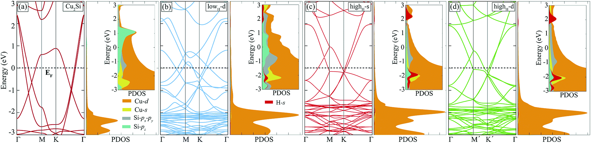 | ||
| Fig. 5 Electronic band structure and PDOS are demonstrated for monolayers of (a) Cu2Si, (b) lowH-d, (c) highH-s, and (d) highH-d. Fermi level, EF, is set to zero. Inset figures of PDOS are rescaled with respect to the number of atoms per unit cell. | ||
To better understand the effect of H atoms on the electronic structure of Cu2Si, we also analyze PDOS of the hydrogenated derivatives. As previously mentioned in Sec. III, the main contribution to the electronic structure around the Fermi level of the material originates from the Cu-d and Si-p orbitals. As seen in the Fig. 5 with increasing amount of hydrogen, the contribution from Si-pz near the Fermi level decreases, and the hybridization between the orbitals of Si-pz and Cu-d decreases. It is clearly seen from the PDOS diagrams of hydrogenated derivatives of the material peak positions and the shapes of the H-s and Si-pz are overlapped which indicate the strong hybridization of these orbitals. As a result, the Si-pz peak in PDOS of the pristine crystal dissolves and moves to lower energies when the structure is hydrogenated. Bonding states of Si–H reside about 2 eV below the EF whereas the anti-bonding states of H-s are 2 eV above the EF. The saturation of the dangling bonds of Si-pz leads reduction of the surface activity of the Cu2Si monolayer. In addition, the calculations reveal that hydrogenated derivatives of the material do not exhibit any net magnetic moment.
V. Conclusions
In this study, we investigated structures of hydrogenated derivatives of Cu2Si monolayer by performing density functional theory-based calculations. The pristine monolayer of Cu2Si composed of coplanar sublattices of hexagonal Cu and trigonal Si was found to be dynamically stable. Electronic structure calculations revealed that the monolayer Cu2Si is a metal with a nonmagnetic ground state.Adsorption of a single H atom on Cu2Si monolayer was examined and the total energy calculations revealed that the most favorable adsorption site of H atom is Si site with a binding energy of −2.80 eV. Diffusion energy barrier and possible migration paths of a single H adsorbed on the structure were determined. Structural optimizations and phonon calculations revealed that there exists three dynamically stable hydrogenated monolayers of Cu2Si. It was found that the planar geometry and the metallic electronic character of the material were not affected by different amounts of hydrogenation and the specific heat of the material at room temperature increases as the amount of hydrogenation increases. Cu2Si monolayer with a planar geometry and robust electronic structure offers a new platform for nanoscale applications.
Conflicts of interest
There are no conflicts to declare.Acknowledgements
Computational resources were provided by TÜBITAK ULAKBİM, High Performance and Grid Computing Center (TR-Grid e-Infrastructure). E. U. and R. T. S. acknowledge financial support from the TÜBITAK through the project 117F131. H. S. acknowledges financial support from the TÜBITAK through the project 117F095.References
- K. S. Novoselov, A. K. Geim, S. V. Morozov, D. Jiang, M. I. Katsnelson, I. V. Grigorieva, S. V. Dubonos and A. A. Firsov, Science, 2004, 306(5696), 666–669 CrossRef CAS PubMed.
- A. Kara, H. Enriquez, A. P. Seitsonen, L. C. L. Y. Voon, S. Vizzini, B. Aufray and H. Oughaddou, Surf. Sci. Rep., 2012, 67(1), 1–18 CrossRef CAS.
- S. Cahangirov, M. Topsakal, E. Akturk, H. Sahin and S. Ciraci, Phys. Rev. Lett., 2009, 102(23), 236804 CrossRef CAS PubMed.
- K. F. Mak, C. Lee, J. Hone, J. Shan and T. F. Heinz, Phys. Rev. Lett., 2010, 105(13), 136805 CrossRef PubMed.
- R. A. Gordon, D. Yang, E. D. Crozier, D. T. Jiang and R. F. Frindt, Phys. Rev. B: Condens. Matter Mater. Phys., 2002, 65(12), 125407 CrossRef.
- S. Tongay, H. Sahin, C. Ko, A. Luce, W. Fan, K. Liu, J. Zhou, Y. S. Huang, C. H. Ho, J. Yan, D. F. Ogletree, S. Aloni, J. Ji, S. Li, J. Li, F. M. Peeters and J. Wu, Nat. Commun., 2014, 5, 3252 CrossRef PubMed.
- K. K. Kim, A. Hsu, X. Jia, S. M. Kim, Y. Shi, M. Hofmann, D. Nezich, J. F. Rodriguez-Nieva, M. Dresselhaus, T. Palacios and J. Kong, Nano Lett., 2012, 12(1), 161–166 CrossRef PubMed.
- H. Sahin, S. Cahangirov, M. Topsakal, E. Bekaroglu, E. Akturk, R. T. Senger and S. Ciraci, Phys. Rev. B: Condens. Matter Mater. Phys., 2009, 80(15), 155453 CrossRef.
- P. Tsipas, S. Kassavetis, D. Tsoutsou, E. Xenogiannopoulou, E. Golias, S. A. Giamini, C. Grazianetti, D. Chiappe, A. Molle, M. Fanciulli and A. Dimoulas, Appl. Phys. Lett., 2013, 103, 251605 CrossRef.
- L.-M. Yang, I. A. Popov, T. Frauenheim, A. I. Boldyrev, T. Heine, V. Bacic and E. Ganz, Phys. Chem. Chem. Phys., 2015, 17(39), 26043–26048 RSC.
- L.-M. Yang, I. A. Popov, A. I. Boldyrev, T. Heine, T. Frauenheim and E. Ganz, Phys. Chem. Chem. Phys., 2015, 17(27), 17545–17551 RSC.
- L.-M. Yang and E. Ganz, Phys. Chem. Chem. Phys., 2016, 18(26), 17586–17591 RSC.
- L.-M. Yang, M. Dornfeld, T. Frauenheim and E. Ganz, Phys. Chem. Chem. Phys., 2015, 17(39), 26036–26042 RSC.
- L.-M. Yang, T. Frauenheim and E. Ganz, J. Nanomater., 2016, 2016, 8429510 Search PubMed.
- L.-M. Yang, V. Bačić, I. A. Popov, A. I. Boldyrev, T. Heine, T. Frauenheim and E. Ganz, J. Am. Chem. Soc., 2015, 137(7), 2757–2762 CrossRef CAS PubMed.
- B. Feng, B. Fu, S. Kasamatsu, S. Ito, P. Cheng, C.-C. Liu, Y. Feng, S. Wu, S. K. Mahatha, P. Sheverdyaeva, P. Moras, M. Arita, O. Sugino, T.-C. Chiang, K. Shimada, K. Miyamoto, T. Okuda, K. Wu, L. Chen, Y. Yao and I. Matsuda, Nat. Commun., 2017, 8(1), 1007 CrossRef PubMed.
- A. A. Burkov, M. D. Hook and L. Balents, Phys. Rev. B: Condens. Matter Mater. Phys., 2011, 84(23), 235126 CrossRef.
- K. Mullen, B. Uchoa and D. T. Glatzhofer, Phys. Rev. Lett., 2015, 115(2), 026403 CrossRef PubMed.
- S.-Y. Yang, H. Yang, E. Derunova, S. S. P. Parkin, B. Yan and M. N. Ali, Adv. Phys.: X, 2018, 3(1), 1414631 Search PubMed.
- M. Yagmurcukardes, C. Bacaksiz, R. T. Senger and H. Sahin, 2D Mater., 2017, 4(3), 035013 CrossRef.
- H. Pan, J. Phys. Chem. C, 2014, 118(24), 13248–13253 CrossRef CAS.
- S. Radhakrishnan, D. Das, A. Samanta, C. A. de los Reyes, L. Deng, L. B. Alemany, T. K. Weldeghiorghis, V. N. Khabashesku, V. Kochat, Z. Jin, P. M. Sudeep, A. A. Martí, C.-W. Chu, A. Roy, C. S. Tiwary, A. K. Singh and P. M. Ajayan, Sci. Adv., 2017, 3(7), e1700842 CrossRef PubMed.
- J. O. Sofo, A. S. Chaudhari and G. D. Barber, Phys. Rev. B: Condens. Matter Mater. Phys., 2007, 75(15), 153401 CrossRef.
- D. C. Elias, R. R. Nair, T. M. Mohiuddin, S. V. Morozov, P. Blake, M. P. Halsall, A. C. Ferrari, D. W. Boukhvalov, M. I. Katsnelson, A. K. Geim and K. S. Novoselov, Science, 2009, 323(5914), 610–613 CrossRef CAS PubMed.
- R. R. Nair, W. Ren, R. Jalil, I. Riaz, V. G. Kravets, L. Britnell, P. Blake, F. Schedin, A. S. Mayorov, S. Yuan, M. I. Katsnelson, H. M. Cheng, W. Strupinski, L. G. Bulusheva, A. V. Okotrub, I. V. Grigorieva, A. N. Grigorenko, K. S. Novoselov and A. K. Geim, Small, 2010, 6(24), 2877–2884 CrossRef CAS PubMed.
- F. Iyikanat, A. Kandemir, H. D. Ozaydin, R. T. Senger and H. Sahin, Nanotechnology, 2017, 28(49), 495709 CrossRef CAS PubMed.
- B. Nemeth, S. P. Harvey, J. V. Li, D. L. Young, A. Upadhyaya, V. LaSalvia, B. G. Lee, M. R. Page and P. Stradins, Energy Procedia, 2017, 124, 295–301 CrossRef CAS.
- J. I. Pankove, in Semiconductors and Semimetals, ed. J. I. Pankove and N. M. Johnson, Elsevier, 1991, vol. 34, 3, pp. 35–47 Search PubMed.
- J. Song, L. Wang, A. Zibart and C. Koch, Metals, 2012, 2(4), 450–477 CrossRef CAS.
- G. Kresse and J. Hafner, Phys. Rev. B: Condens. Matter Mater. Phys., 1993, 47(1), 558–561 CrossRef CAS.
- G. Kresse and J. Hafner, Phys. Rev. B: Condens. Matter Mater. Phys., 1994, 49(20), 14251 CrossRef CAS.
- J. P. Perdew, K. Burke and M. Ernzerhof, Phys. Rev. Lett., 1996, 77(18), 3865 CrossRef CAS PubMed.
- S. Grimme, J. Comput. Chem., 2006, 27(15), 1787–1799 CrossRef CAS PubMed.
- D. Alfe, Comput. Phys. Commun., 2009, 180(12), 2622–2633 CrossRef CAS.
- G. Henkelman, A. Arnaldsson and H. Jónsson, Comput. Mater. Sci., 2006, 36(3), 354–360 CrossRef.
- R. F. W. Bader, Atoms in Molecules A Quantum Theory, Oxford University Press, Oxford, U.K., 1990 Search PubMed.
- J. Zhou, Q. Wang, Q. Sun, X. S. Chen, Y. Kawazoe and P. Jena, Nano Lett., 2009, 9(11), 3867–3870 CrossRef CAS PubMed.
- W. Kohn, Phys. Rev. Lett., 1959, 2(9), 393–394 CrossRef CAS.
- D. L. Nika and A. A. Balandin, J. Phys.: Condens. Matter, 2012, 24(23), 233203 CrossRef PubMed.
- V. N. Popov, Phys. Rev. B: Condens. Matter Mater. Phys., 2003, 67(8), 085408 CrossRef.
- A. Molina-Sánchez and L. Wirtz, Phys. Rev. B: Condens. Matter Mater. Phys., 2011, 84(15), 155413 CrossRef.
- R. A. Ballinger and N. H. March, Nature, 1954, 174, 179 CrossRef CAS.
- A. H. Mahan, J. Carapella, B. Nelson, R. Crandall and I. Balberg, J. Appl. Phys., 1991, 69, 6728 CrossRef CAS.
- R. E. I. Schropp, Thin Solid Films, 2015, 595, 272–283 CrossRef CAS.
- A. Felten, D. McManus, C. Rice, L. Nittler, J.-J. Pireaux and C. Casiraghi, Appl. Phys. Lett., 2014, 105, 183104 CrossRef.
- C. Kittel, Introduction to Solid State Physics, Wiley, New York, 1996 Search PubMed.
- T. Tohei, A. Kuwabara, F. Oba and I. Tanaka, Phys. Rev. B: Condens. Matter Mater. Phys., 2006, 73(6), 064304 CrossRef.
- See ESI‡ for the phonon spectra of dynamically unstable hydrogenated derivatives of Cu2Si.
Footnotes |
| † PACS numbers: 71.15.Mb, 61.72.Ww, 63.20.Dj, 63.20.dk, 65.40.Ba, 73.22.-f. |
| ‡ Electronic supplementary information (ESI) available. See DOI: 10.1039/c8ra07824f |
| This journal is © The Royal Society of Chemistry 2018 |