
 Open Access Article
 This Open Access Article is licensed under a Creative Commons Attribution-Non Commercial 3.0 Unported Licence
Rapid fabrication of porous silicon/carbon microtube composites as anode materials for lithium-ion batteries
Shuxian Wang a,
Chunlai Huangab,
Lei Wang*a,
Wei Sunc and
Deren Yanga
a,
Chunlai Huangab,
Lei Wang*a,
Wei Sunc and
Deren Yanga
aState Key Laboratory of Silicon Materials, School of Materials Science and Engineering, Zhejiang University, Hangzhou 310027, P. R. China. E-mail: phy_wangl@zju.edu.cn
bJiangsu Key Lab of Silicon Based Electronic Materials, Jiangsu GCL Silicon Material Technology Development Co., Ltd., Xuzhou, 221000, P. R. China
cBengbu Institute of Product Quality Supervision and Inspection Research, Bengbu, Anhui 233000, P. R. China
First published on 7th December 2018
Abstract
Herein, we present a simple and rapid method to synthesize porous silicon/carbon microtube composites (PoSi/CMTs) by adopting a unique configuration of acid etching solution. The CMTs can act as both conductive agent and buffer for Si volume change during the charge and discharge process. The highly reversible capacity and excellent rate capability can be ascribed to the structure, where porous silicon powders are wrapped by a network of interwoven carbon microtubes. The composites show specific capacities of more than 1712 mA h g−1 at a current density of 100 mA g−1, 1566 mA h g−1 at 200 mA g−1, 1407 mA h g−1 at 400 mA g−1, 1177 mA h g−1 at 800 mA g−1, 1107 mA h g−1 at 1000 mA g−1, 798 mA hg−1 at 2000 mA g−1, and 581 mA h g−1 at 3000 mA g−1 and maintain a value of 1127 mA h g−1 after 100 cycles at a current density of 200 mA g−1. Electrochemical impedance spectroscopy (EIS) measurements prove that charge transfer resistance of PoSi/CMT composites is smaller than that of pure PoSi. In this study, we propose a quick, economical and feasible method to prepare silicon-based anode materials for lithium-ion batteries.
Introduction
Lithium-ion batteries have attracted increasing attention due to their prospective industrial applications. At present, lithium-ion batteries occupy significant market shares of mobile phones, notebook computers, new energy vehicles, energy storage power stations, etc.1,2 The current commercial lithium anode material is graphite, and its theoretical capacity is only 372 mA h g−1,3 which cannot meet the requirement of high energy density. To improve the energy density of weight and volume,4,5 various electrochemical active materials with high capacity have been investigated to replace graphite as anode materials of lithium-ion batteries.According to different reaction mechanisms, the anode materials of lithium-ion batteries can be divided into three types: alloy reactive type, embedded type and structural transformation type.6 Among the alloy reactive materials, lithium–silicon alloy shows the greatest utilization potential, because the theoretical discharge capacity of Li4.4Si alloy is as high as 4200 mA h g−1.7 Besides, it has the advantages of low discharge voltage and rich reserves in natural resources. However, in the process of charging, the insertion of lithium ions causes volume expansion of silicon, which can reach 3.2 times that of the original volume. Huge volume expansion/constriction can cause great stress, which results in crushing and cracking of silicon materials; they instantly lose their effective electronic conduction, and this leads to rapid attenuation of the capacity. Moreover, the diffusion coefficient of lithium in a lithium–silicon alloy is small; therefore, the conductivity of silicon is poor.
To solve the problem of poor conductivity of silicon, different carbon materials such as carbon nanotubes8–11 and graphene12–14 are often introduced into silicon anodes. Aiming to solve the problem of capacity instability caused by volume expansion of silicon, various methods such as carbon encapsulation and the preparation of nano silicon and porous silicon have been investigated. Besides, to promote electrical or thermal stability, porous Si materials have been designed to combine with conducting polymer and transition metal oxides.15–19 Among these methods, the de-alloying method is a useful way for preparing porous silicon with high electrochemical performance. Recently, Al–Si alloy has attracted much attention due to its low cost. Jiang et al.20 used an acidic etching solution to remove aluminium from aluminium–silicon (Al–Si) alloys, leaving behind the silicon framework, which was porous silicon. Jinkui Feng et al.21 reacted Al–Si alloys with HCl in a graphene oxide solution, and the graphene oxide was reduced to graphene in a hydrogen atmosphere after filtration. Therefore, porous silicon/graphene composites were prepared, and their capacity remained at 2000 mA h g−1 after 100 cycles. Takeshi Wada et al.22 synthesized nano porous silicon using dealloying in a metallic melt, which is a top-down process. When immersing Mg2Si precursor in a Bi melt, Mg can selectively dissolved from Mg2Si into the Bi melt, by the principle that Mg and Bi were solid solution to each other and Si and Bi were not solid solution to each other. Park et al.23 synthesized porous silicon by chemical etching of melt-spun Si/Al–Cu–Fe alloy nanocomposites followed by carbonization using a pitch. The composite material still exhibited a capacity of 1000 mA h g−1 or more after 100 cycles. The above study shows some advantages of the de-alloying method to obtain porous Si anode materials. However, it is still a challenge for the de-alloying process of Al–Si alloy to rapidly remove Al from Si alloy by easy chemical etching to attain a stable porous Si structure.
In this paper, we proposed a unique configuration of acid etching solution to resolve the problem of very long preparation time and incomplete removal of aluminium from Al–Si alloys; we design a simple and easy method to synthesize PoSi/CMTs, which is of great help in industrial applications because of reduction in time. In addition, the spherical Al–Si alloys were employed to avoid the problem of easy collapse of the bulk porous silicon structure. This method is simple and feasible, which can be used to prepare PoSi/CMTs with high stability and good conductivity as anode materials for lithium-ion batteries.
Experimental
Synthesis of porous silicon/carbon microtube composites
The schematic process of experiments is shown in Fig. 1. A certain amount of Al–Si alloy powders (consisting of 80% Al, 20% Si, National Drug Chemical Reagents Co., Ltd) was added into 4.8 mol L−1 HCl (AR), and a proper amount of CuCl2·2H2O (AR, Aldrich) was added along with constant magnetic stirring. After aluminium was removed (about 2 h), the composites were washed with deionized water for three times. After that, a mixture of porous silicon and copper particles was obtained by filtering and drying the sample in a vacuum oven at 80 °C. Then, the sample was placed in a tube furnace on a crucible and heat-treated at 750 °C for 3 hours with the mix gas (Ar![[thin space (1/6-em)]](https://www.rsc.org/images/entities/char_2009.gif) :C2H2 = 10:1; the heating rate of the furnace is 8 °C min−1). Finally, the copper was removed from the product by 8.5 mol L−1 HNO3 (AR).
:C2H2 = 10:1; the heating rate of the furnace is 8 °C min−1). Finally, the copper was removed from the product by 8.5 mol L−1 HNO3 (AR).
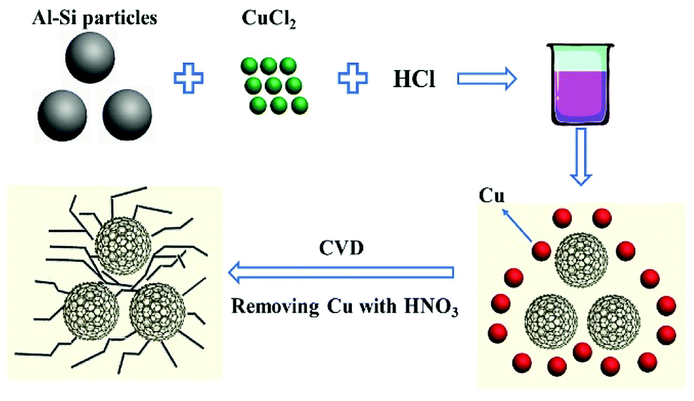 | ||
| Fig. 1 Schematic illustration for the synthesis of PoSi/CMT particles. | ||
Characterization and electrochemical measurement
The morphology of the samples was characterized by a field emission scanning electron microscope (FESEM, HITACHI S4800, the operating voltage is 5 kV) and a field emission transmission electron microscope (FEI TECNAI G2 F20, the operating voltage is 200 kV). X-ray diffraction (XRD) was performed on a Rigaku D/max-ga X-ray diffractometer with graphite monochromatized Cu Kα radiation (λ = 1.54178 Å). The Raman analysis was conducted by a Jobin-Yvon's Lab Raman HR-800 UV laser Raman spectrometer. The argon source used for the test was 10 mW with a wavelength of 514.5 nm. Brunauer–Emmett–Teller (BET) specific surface area and pore diameter distribution were determined from the results of N2 adsorption/desorption measurements using a Beckman Coulter Omnisorp 100cx. Thermogravimetric analysis (TGA) was conducted with SDT Q600 V8.2 Build 100. Active materials (PoSi/CMTs), sodium carboxymethyl cellulose (CMC) and conductive agent (SP) were mixed at a mass ratio of 7:2:1 and stirred for 12 hours with deionized water. About 2 mg of active material was coated on the copper foam. The electrode was placed in an argon-filled glovebox (Mbraun, Labstar, Germany) and assembled into a coin cell (2025-type) using a lithium foil as a counter electrode. The electrolyte was 1 M LiPF6 in the mixture of dimethyl carbonate (DMC) and ethylene carbonate (EC) (1:1 at volume ratio); 5 vol% fluoroethylene carbonate was added to improve the cycling stability. All cells were cycled between 0.01 and 1.5 V. The charge and discharge tests were performed in a Land battery test system (CT2001A of Wuhan Lanhe Electronics Co., Ltd.). The test system was equipped with a thermostat and a constant temperature of 35 °C. For cyclic voltammetry, we used the LK2006A electrochemical workstation from Tianjin Lanli Chemical Electronic High Technology Co., Ltd.
Results and discussion
There are many reports about the de-alloying of Al–Si alloy by acid etching.20,21,24 The key point is how to remove aluminum efficiently and to the utmost extent. It is difficult to quickly and completely remove Al from Al–Si alloy with individual acid by traditional methods. Moreover, the porous structure of silicon after de-alloying can be destroyed by continuous stirring for a long time during the acid reaction. In this paper, we proposed to add CuCl2 as an etching promoter in the etchant HCl (the molar ratios of Al and CuCl2 are 12:1, 6:1, 3:1 and 1.5:1). Copper ions have weak oxidizing properties and can enter the Al–Si alloy to make the reaction more complete. More importantly, the addition of CuCl2 can reduce the reaction time from more than 24 hours to 2 hours. The reduction of time is very important for industrial applications. Additionally, the porous silicon prepared by the CuCl2-assisted process has better chemical properties, which will be discussed below. XRD patterns of Al–Si alloys after etching with different proportions of CuCl2 in the etchant HCl are shown in Fig. 2a. It can be seen that not only Cu, but also Cu2O is obtained, whereas only Cu is effective for the next-step process to produce CMTs. Furthermore, more Cu and less Cu2O are obtained when the molar ratio of Al and CuCl2 is 6:1. We can speculate that the following reactions occur during etching of the Al–Si alloy:| Al + HCl → AlCl3 + H2 | (1) |
| Al + CuCl2 → AlCl3 + Cu | (2) |
| Cu + O2 → CuO | (3) |
| Cu + CuO → Cu2O | (4) |
| CuO + HCl → CuCl2 + H2O | (5) |
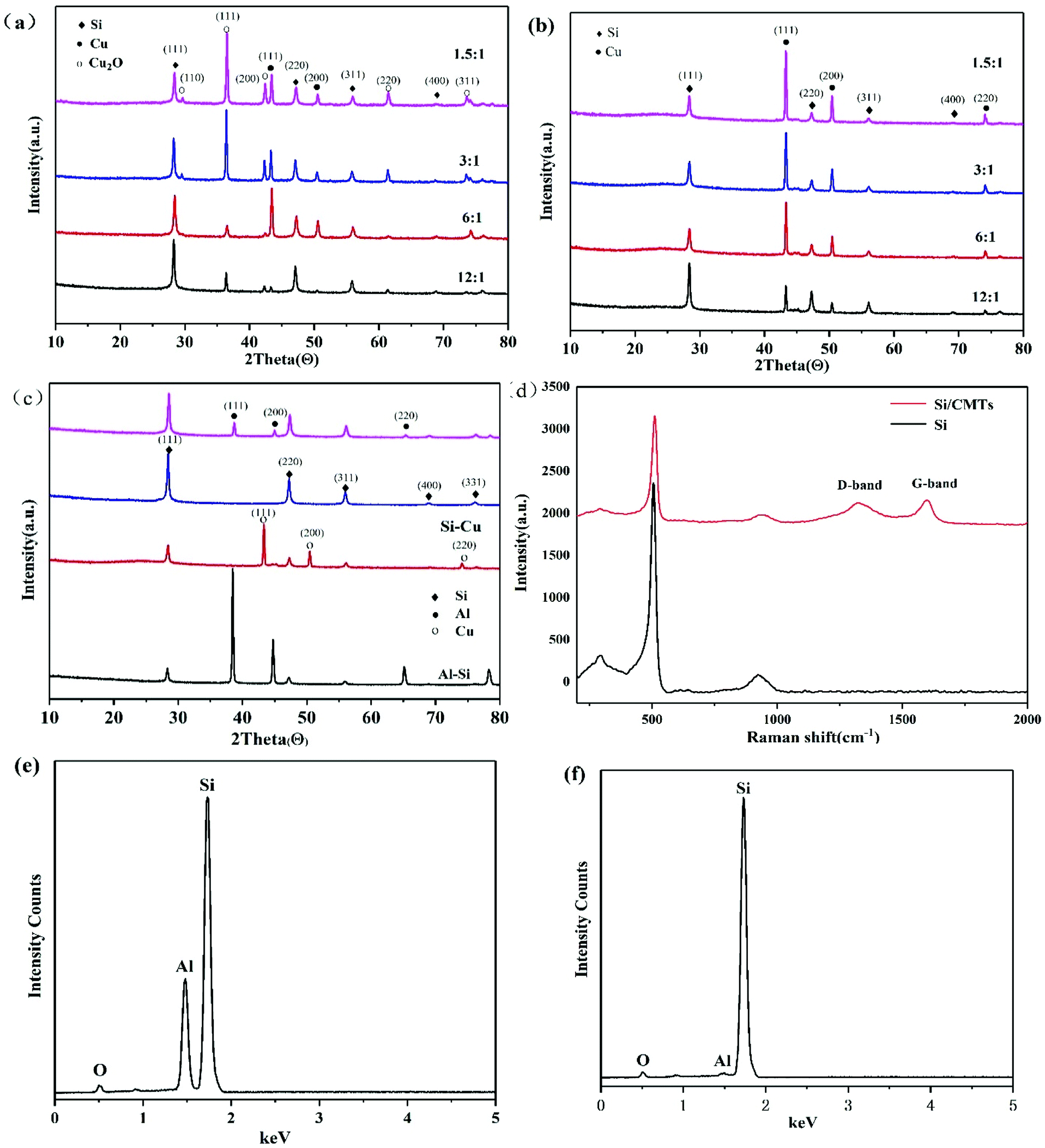 | ||
| Fig. 2 XRD patterns of (a) Al–Si alloys after etching with different proportions of CuCl2 in the etchant HCl; (b) samples after chemical vapor deposition; (c) Al–Si alloys that have undergone different processing steps. (d) Raman spectra of Si and PoSi/CMTs. EDX patterns of (e) Al–Si alloys after etching with HCl for 2 h; (f) Al–Si alloys after etching with CuCl2 and HCl for 2 h (the molar ratio of Al and CuCl2 is 6:1). | ||
Copper ions are weakly oxidizing and can oxidize aluminium to aluminium ions; thus, copper ions can be reduced to copper. CuO formed during the reaction is etched by HCl to form CuCl2 again, as shown in eqn (5). This process continues until aluminium is eliminated. Residual copper in the form of an elementary substance or Cu2O can be easily removed by acid, which is removed after chemical vapour deposition because copper can be used as a catalyst for CMT formation. XRD patterns of samples after chemical vapour deposition in mixed gas are shown in Fig. 2b, which shows that Cu2O species in the samples are reduced to Cu by C2H2. Fig. 2c shows the XRD pattern of Al–Si alloys that have undergone different processing steps. The first curve in Fig. 2c corresponds to the experiment in which only HCl is used to remove Al for 2 hours, and the second curve corresponds to the experiment in which both HCl and CuCl2 are used to remove Al for 2 hours. Combined with the EDX patterns in Fig. 2e and f, it can be seen that the peak of aluminium can hardly be detected with the addition of CuCl2, indicating that aluminium is removed with the addition of CuCl2. After chemical vapour deposition, Cu is removed by nitric acid. Compared with the observation in the third curve in Fig. 2c, there is no copper peak in the second curve, indicating that Cu has also been removed. Fig. 2d shows the Raman spectra of Si and PoSi/CMT composites. For the PoSi/CMT composites, the curve has a highest peak at 511 cm−1, which is consistent with the characteristic peak of pure silicon.25 The peaks at around 1340 cm−1 and 1590 cm−1 (ref. 26) correspond to the disordered carbon or defect band (D band) and graphitic carbon band (G band). The D band is related to disorder-allowed phonon modes, which becomes Raman active as a result of lack of long-range order in amorphous graphitic materials; the G band is associated with the allowed E2g optical modes of the Brillouin zone centre of crystalline graphite.27 It is generally accepted that the integrated intensity ratio of the D band and G band, i.e., ID/IG depends on the structural characteristics of carbon.28 In the experiment, the ID/IG ratio of PoSi/CMTs is calculated to be 2.1, suggesting high disorder of CMT materials.
The morphology and detailed microstructure of Al–Si, porous Si, CMT, and PoSi/CMT samples were investigated by FE-SEM and FE-TEM. As indicated in Fig. 3a, the as-received Al–Si alloy particles are spherical with diameters of several micrometres. Fig. 3b shows a mixture of porous silicon, Cu and Cu2O after the dealloying process. As seen from the figure, most of the porous silicon particles maintain a spherical structure; only a few of the spheres are broken, which is caused by tension produced by hydrogen gas released during dealloying. The morphology of porous silicon depends on the distribution of silicon in Al–Si alloys, most of which exhibit a network-like silicon structure. The angular and cubic particles that are agglomerated in the figure are Cu and Cu2O.29,30 After chemical vapor deposition, a large number of tubes (about 1 μm in diameter) are produced and interlaced between the network-like silicon frameworks, as shown in Fig. 3c and d. Combined with the Raman analysis, we can infer that the generated tubes are carbon microtubes. From the XRD results, Cu particles are formed after etching, resulting in the formation of carbon microtubes in the CVD process.31 However, since the crystalline peaks of carbon are not apparent in the XRD pattern, it is speculated that the carbon microtubes are amorphous. TEM images of the bent, coiled carbon microtubes are shown in Fig. 3e, the diameter of which is about 0.5–1 μm. Fig. 3f shows the three-dimensional structure of Si/CMT composite in which carbon microtubes are coiled on the surface of silicon particles. Selected area electron diffraction (SAED) modes for microtubes are presented in Fig. 3g; the diffuse pattern shows that the CMTs have typical amorphous features.
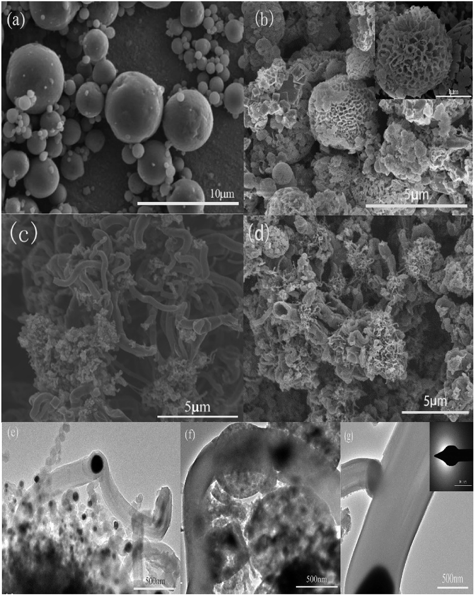 | ||
| Fig. 3 SEM images of Al–Si alloy particles (a), porous silicon/Cu/Cu2O after etching (b) and PoSi/CMTs (c and d); TEM images of bent, coiled CMTs (e), PoSi/CMTs (f), and a CMT with the selected area electron diffraction (SAED) pattern in the inset (g). | ||
Fig. 4a–d show the TGA profiles of PoSi/CMTs fabricated with different proportions of CuCl2. There are two peaks in the TGA profiles, corresponding to a two-step decomposition of carbon material. The antioxidant capacity of the substance is related to the molecular structure of these carbon materials. CMTs and amorphous carbon are composed of sp2 carbon and sp3 carbon.32,33 The bond energy of sp2 carbon is higher than that of sp3 carbon; thus, sp2 carbon is thermodynamically more stable.34 Therefore, we speculate that 400–480 °C may mostly correspond to sp3 carbon, and 480–650 °C may mostly correspond to sp2 carbon. Except the mass ratios for the first group of samples, the mass ratios of CMTs and amorphous carbon are higher than 30%. This has a slight negative effect on the capacity of PoSi/CMT composites but greatly increases the stability of capacity. Nitrogen adsorption–desorption measurements at 77 K are performed, as shown in Fig. 4e. The specific surface area of porous silicon is about 97 m2 g−1. The pore size distribution curve (Fig. 4f) shows that most of the pores have diameters of less than 100 nm, and pore diameter of 20 nm is especially common. In the process of deintercalation/intercalation of lithium, a large number of nanopores not only increase the specific surface area of the material, which can allow the active material to contact the electrolyte quickly and easily, but also effectively relieve the stress caused by the volume expansion and contraction. In addition, the nanoscale pores can effectively shorten the lithium-ion diffusion distance and improve the material's rate performance; therefore, they exhibit more excellent performance.
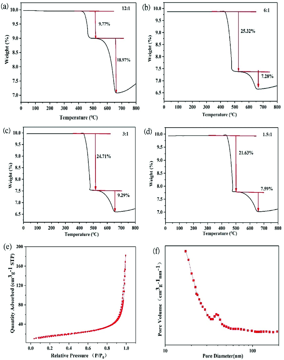 | ||
| Fig. 4 Thermal stability curves (under compressed air gas) of (a) PoSi/CMTs when the molar ratio of Al and CuCl2 is 12:1; (b) PoSi/CMTs when the molar ratio of Al and CuCl2 is 6:1; (c) PoSi/CMTs when the molar ratio of Al and CuCl2 is 3:1; (d) PoSi/CMTs when the molar ratio of Al and CuCl2 is 1.5:1. (e) Typical nitrogen adsorption–desorption curve of porous silicon. (f) Pore size distribution plot of porous silicon. | ||
Galvanostatic charge and discharge measurements were performed to evaluate the capacity and cycling life of PoSi/CMTs and Si at a current density of 200 mA g−1 between 0.01 and 1.5 V. For comparison, part of charge–discharge voltage curves of PoSi/CMTs and Si is shown in Fig. 5a and b. From Fig. 5a, we can see lower and longer plateaus in the first discharge cycle due to the lithium alloying behaviour of crystalline silicon. Since silicon becomes amorphous after the first charge–discharge cycle, the shape of the curve will change and most of the curves overlap later in the cycle. The PoSi/CMT electrode demonstrates first reversible capacity of 2344 mA h g−1 with the first coulomb efficiency of 66%. As a comparison, the initial reversible capacity of blank Si is 2315 mA h g−1 and the first coulombic efficiency is 62%. Clearly, PoSi/CMTs possess better specific capacity retention than blank Si because visible porous structures and CMTs can buffer the volume change. The low first coulomb efficiency can be due to the formation of the solid electrolyte interphase on the surface of the electrode35 and the irreversible loss of lithium at the first lithiation process such as electrolyte decomposition on carbon.36 Cycle performances of PoSi/CMTs and Si at a current density of 200 mA g−1 are displayed in Fig. 5c; all electrodes are cycled between 0.01 and 1.5 V at a current density of 200 mA g−1 for 100 cycles. For PoSi/CMTs, the first specific capacity is 2344 mA h g−1, and the second specific capacity is 1545 mA g−1. The reversible capacity of PoSi/CMT electrode remains at 1127 mA h g−1 after 100 cycles (73% capacity retention). However, only a capacity of 283 mA h g−1 remains after 100 cycles for the blank silicon electrode. This is mainly due to the following reasons: (1) the porous structure buffers the volume expansion during the charge and discharge process. (2) The amorphous carbon layer on the porous silicon surface can reduce direct contact between the electrolyte and silicon, thus reducing irreversible lithium loss. (3) Carbon microtubes and amorphous carbon layers not only improve the conductivity but also provide some mitigation of volume expansion.37
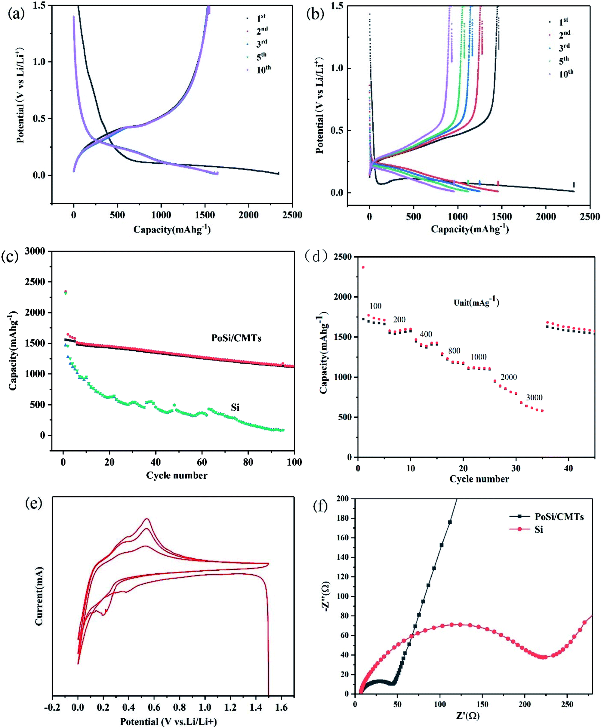 | ||
| Fig. 5 Part of charge–discharge voltage curves of (a) PoSi/CMTs; (b) Si at 200 mA g−1 from 0.01 to 1.5 V. (c) Cycle performances of the PoSi/CMTs and Si at a current density of 200 mA g−1. (d) Rate performance of PoSi/CMTs and Si at current densities of 100, 200, 400, 800, 1000, 2000 and 3000 mA g−1. (e) Cyclic voltammograms of PoSi/CMTs in a scanning range of 0.01–1.5 V and at a scanning rate of 0.1 mV s−1. (f) Electrochemical impedance spectroscopy of PoSi/CMTs and Si. | ||
In addition to good capacity retention, PoSi/CMT electrodes also demonstrate excellent rate capability, as shown in Fig. 5d. When the current density increases from 100 mA g−1 to 200, 400, 800, 1000, 2000, and 3000 mA g−1, the reversible capacities of PoSi/CMTs correspond to 1712 mA h g−1, 1566 mA h g−1, 1407 mA h g−1, 1177 mA h g−1, 1107 mA h g−1, 798 mA h g−1, and 581 mA h g−1. The superior rate performances of the PoSi/CMT electrodes are due to the porous structure of silicon and higher electrical conductivity of CMTs, which greatly reduce not only the internal resistance of electrode but also the fracture of electrode active materials. Cyclic voltammograms of PoSi/CMTs in a scanning range of 0.01–1.5 V and at a scanning rate of 0.1 mV s−1 are shown in Fig. 5e. It is shown from the first negative scan that the irreversible peak of electrolyte decomposition ranging from 0.5 to 1.1 V barely appears, which indicates that the electrolyte decomposition on the surface is inhibited by the amorphous carbon coating on silicon.38 Cycle peak increases below 0.3 V and corresponds to the cathodic lithiation of crystalline Si to form LixSi. In the positive scan, both the anodic peaks at 0.3 V and 0.5 V correspond to the delithiation of LixSi back to Si. The cathodic peak appearing between 0.3 V and 0.1 V in the second cycle is mainly caused by the intercalation of amorphous carbon and amorphous silicon. The peaks at 0.3 V and 0.5 V and the peak between 0.3 V and 0.1 V become broader and stronger gradually after the initial cycle owing to the gradual activation of Si and degradation of Si crystallinity. To better comprehend the superior electrochemical performance of PoSi/CMTs compared with that of blank Si, EIS at the open-circuit voltage is performed (Fig. 5f). The high-frequency semicircle is in accordance with the charge-transfer resistance (Rct) and double-layer capacitance at the interface between the electrolyte and electrode. The angle of the inclined line corresponds to the rate of lithium-ion diffusion process.39,40 The semicircle diameter of PoSi/CMTs is smaller than that of blank silicon, indicating that PoSi/CMTs have smaller charge transfer resistance. These experimental results demonstrate that CMTs and amorphous carbon layers can increase the rate of electron transport, thus increasing the rate of intercalation and deintercalation of lithium ions. Therefore, PoSi/CMTs display excellent electrochemical performance with stable cycle performance and superior rate performance.
In addition, we also compared the cyclic properties of porous silicon materials prepared by conventional etching processes and those of porous silicon materials prepared by CuCl2-assisted process, as shown in Fig. 6. For the porous silicon materials prepared by CuCl2-assisted process, the first specific capacity is 2963 mA h g−1, and the second specific capacity is 1880 mA g−1. The reversible capacity drops to 945 mA h g−1 after 50 cycles (50% capacity retention). Compared with the capacity retention ratio of 73% of PoSi/CMTs, it is indicated that CMTs and amorphous carbon do contribute to the increase in the stability of the porous silicon. However, for porous silicon prepared by a conventional etching process, the first specific capacity is 2173 mA h g−1, and the second specific capacity is 1351 mA g−1. The reversible capacity drops to 393 mA h g−1 after 50 cycles. The reason for the low capacity of porous silicon prepared by the conventional process is that the aluminium removal is incomplete.
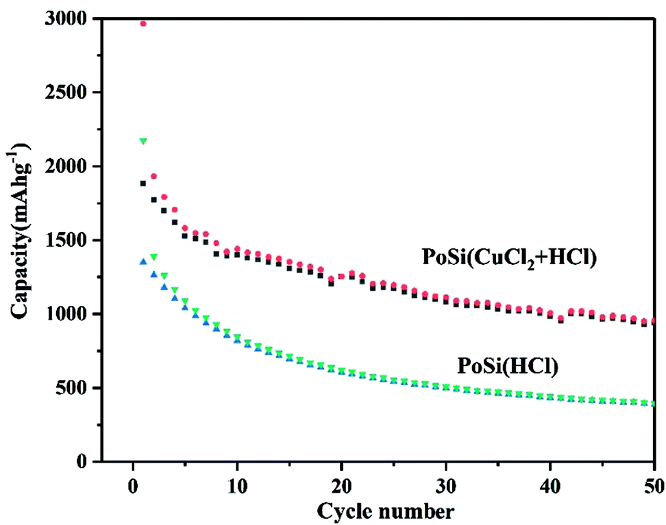 | ||
| Fig. 6 Cycle performances of the porous silicon prepared by different processes at a current density of 200 mA g−1. | ||
Conclusion
A simple and rapid method to synthesize PoSi/CMTs from Al–Si alloy powders is proposed including three main steps: HCl and CuCl2 solution etching, CVD treatment by Ar and C2H2 mix gas and HNO3 cleaning. The products have a stable porous structure and negligible metal residues. CMTs can act as both conductive agent and buffer for Si volume change during the charge and discharge process. The prototype battery device shows high reversible capacity and excellent rate capability, which can be ascribed to the structure, where porous silicon powders are wrapped by a network of interwoven carbon microtubes and amorphous carbon layers.Conflicts of interest
There are no conflicts to declare.Acknowledgements
This work was supported by the National Science Foundation of China (No. 51532007, 61721005), the Fundamental Research Funds for the Central Universities (No. 2017FZA4005) and Key Project of Zhejiang Province (No. 2018C01034).Notes and references
- B. Scrosati, J. Hassoun and Y.-K. Sun, Energy Environ. Sci., 2011, 4, 3287–3295 RSC.
- Y. Hu and X. Sun, J. Mater. Chem. A, 2014, 2, 10712–10738 RSC.
- X. Zuo, J. Zhu, P. Müller-Buschbaum and Y.-J. Cheng, Nano Energy, 2017, 31, 113–143 CrossRef CAS.
- Y.-S. He, P. Gao, J. Chen, X. Yang, X.-Z. Liao, J. Yang and Z.-F. Ma, RSC Adv., 2011, 1, 958–960 RSC.
- M. Ge, X. Fang, J. Rong and C. Zhou, Nanotechnology, 2013, 24, 422001 CrossRef CAS PubMed.
- M. R. Palacin, Chem. Soc. Rev., 2009, 38, 2565–2575 RSC.
- D. Molina Piper, T. Evans, S. Xu, S. C. Kim, S. S. Han, K. L. Liu, K. H. Oh, R. Yang and S. H. Lee, Adv. Mater., 2016, 28, 188–193 CrossRef CAS PubMed.
- H. Wu, G. Zheng, N. Liu, T. J. Carney, Y. Yang and Y. Cui, Nano Lett., 2012, 12, 904–909 CrossRef CAS PubMed.
- W. Weng, H. Lin, X. Chen, J. Ren, Z. Zhang, L. Qiu, G. Guan and H. Peng, J. Mater. Chem. A, 2014, 2, 9306 RSC.
- Y. Li, M. Li, M. Pang, S. Feng, J. Zhang and C. Zhang, J. Mater. Chem. C, 2015, 3, 5573–5579 RSC.
- C. Zhai, N. Du, H. Zhang, J. Yu, P. Wu, C. Xiao and D. Yang, Nanoscale, 2011, 3, 1798–1801 RSC.
- X. Zhao, C. M. Hayner, M. C. Kung and H. H. Kung, Adv. Energy Mater., 2011, 1, 1079–1084 CrossRef CAS.
- N. Lin, J. Zhou, Y. Zhu and Y. Qian, J. Mater. Chem. A, 2014, 2, 19604–19608 RSC.
- L. Shi and T. Zhao, J. Mater. Chem. A, 2017, 5, 3735–3758 RSC.
- J.-G. Kim, G. Jeong, M.-S. Park, M. Seo, S. M. Hwang, Y.-U. Kim, Y.-J. Kim, J. H. Kim and S. X. Dou, ACS Nano, 2014, 8, 2977–2985 CrossRef PubMed.
- H. Y. Eunjun Park, J. Lee, M.-S. Park, Y.-J. Kim and H. Kim, ACS Nano, 2015, 9, 7690–7696 CrossRef PubMed.
- E. Park, J. Kim, D. J. Chung, M. S. Park, H. Kim and J. H. Kim, ChemSusChem, 2016, 9, 2754–2758 CrossRef CAS PubMed.
- J. Kim, J. H. Kim and K. Ariga, Joule, 2017, 1, 739–768 CrossRef CAS.
- H. Jung, Y.-U. Kim, M.-S. Sung, Y. Hwa, G. Jeong, G.-B. Kim and H.-J. Sohn, J. Mater. Chem., 2011, 21, 11213–11216 RSC.
- Z. Jiang, C. Li, S. Hao, K. Zhu and P. Zhang, Electrochim. Acta, 2014, 115, 393–398 CrossRef CAS.
- J. Feng, Z. Zhang, L. Ci, W. Zhai, Q. Ai and S. Xiong, J. Power Sources, 2015, 287, 177–183 CrossRef CAS.
- T. Wada, T. Ichitsubo, K. Yubuta, H. Segawa, H. Yoshida and H. Kato, Nano Lett., 2014, 14, 4505–4510 CrossRef CAS PubMed.
- H. I. Park, M. Sohn, D. S. Kim, C. Park, J. H. Choi and H. Kim, ChemSusChem, 2016, 9, 834–840 CrossRef CAS PubMed.
- W. Zhai, Q. Ai, L. Chen, S. Wei, D. Li, L. Zhang, P. Si, J. Feng and L. Ci, Nano Res., 2017, 10, 4274–4283 CrossRef CAS.
- J. Bonse, K. W. Brzezinka and A. J. Meixner, Appl. Surf. Sci., 2004, 221, 215–230 CrossRef CAS.
- M. Yoshikawa, G. Katagiri, H. Ishida, A. Ishitani and T. Akamatsu, Appl. Phys. Lett., 1988, 52, 1639–1641 CrossRef CAS.
- H. S. Zhu, J. T. Jiu, F. Qiang, W. Hao and C. B. Cao, J. Mater. Sci., 2003, 38, 141–145 CrossRef CAS.
- J. Kastner, T. Pichler, H. Kuzmany, S. Curran, W. Blau, D. N. Weldon, M. Delamesiere, S. Draper and H. Zandbergen, Chem. Phys. Lett., 1994, 221, 53–58 CrossRef CAS.
- F. Fievet, F. Fievet-Vincen, J.-P. Lagier, B. Dumont and M. Figlarz, J. Mater. Chem., 1998, 3, 627–632 RSC.
- R. Bakthavatsalam and J. Kundu, CrystEngComm, 2017, 19, 1669–1679 RSC.
- Y. Han, J. Zhou, J. Dong and K. Yoshiyuki, Phys. Chem. Chem. Phys., 2013, 15, 17171–17178 RSC.
- X. Wang, X. Liu, L. Lai, S. Li, J. Weng, Z. Zhou, Q. Cui, X. Chen, M. Cao and Q. Zhang, Adv. Funct. Mater., 2008, 18, 1809–1823 CrossRef CAS.
- K. Sato, M. Noguchi and A. Demachi, Science, 1994, 264(5158), 556–558 CrossRef CAS PubMed.
- G. Dearnaley, Phys. Bull., 1980, 31, 359 CrossRef.
- M. N. Obrovac and V. L. Chevrier, Chem. Rev., 2014, 114, 11444–11502 CrossRef CAS PubMed.
- S. H. Ng, J. Wang, D. Wexler, K. Konstantinov, Z. P. Guo and H. K. Liu, Angew. Chem., Int. Ed. Engl., 2006, 45, 6896–6899 CrossRef CAS PubMed.
- L. Shen, Z. Wang and L. Chen, RSC Adv., 2014, 4, 15314–15318 RSC.
- M. Yoshio, H. Y. Wang, K. Fukuda, T. Umeno, N. Dimov and Z. Ogumi, J. Electrochem. Soc., 2002, 149, A1598–A1603 CrossRef CAS.
- F. Maroni, R. Raccichini, A. Birrozzi, G. Carbonari, R. Tossici, F. Croce, R. Marassi and F. Nobili, J. Power Sources, 2014, 269, 873–882 CrossRef CAS.
- S. A. Klankowski, G. P. Pandey, B. A. Cruden, J. Liu, J. Wu, R. A. Rojeski and J. Li, J. Power Sources, 2015, 276, 73–79 CrossRef CAS.
| This journal is © The Royal Society of Chemistry 2018 |