DOI:
10.1039/C8RA07343K
(Paper)
RSC Adv., 2018,
8, 41587-41593
Modifying spin current filtering and magnetoresistance in a molecular spintronic device†
Received
3rd September 2018
, Accepted 28th November 2018
First published on 12th December 2018
Abstract
The zigzag edged graphene nanoribbon (ZGNR) is excellent for spintronics devices, and many efforts have been made to investigate its properties such as spin filtering, rectification and magnetoresistance. Here we propose a molecular spintronic transport device based on two ZGNR electrodes connected with a dibenzo[a,c]dibenzo[5,6:7,8]quinoxalino[2,3-i]phenazine (DDQP) molecule. By performing first-principles electron transport computations, we found an enhanced spin polarized current–voltage curve, giant spin filter efficiency, magnetoresistance and rectification ratio properties of the device compared to its all-carbon molecular analogue. Our systematic investigation suggests the vital role played in spin polarized electron transport by nitrogen atoms in DDQP, the ZGNR probe's width and terminal geometry, especially the increased spin filter efficiency with higher ZGNR width.
Introduction
Size minimization of low-dimensional electronic devices has been improved by employing the top-down and bottom-up fabrication methods. Ultimately, we need to precisely confine atoms in the molecular component for a junction's electronic properties. So far such devices could be made by break-junction experiments1 or self-assembling monolayers of molecules in polymeric micro- and nanoporous materials.2,3 To restrain the possible electrode contact fluctuation, carbon-based materials such as carbon nanotubes (CNTs) or graphene, may be qualified as better electrodes than normal metals.4 Many successful experiments and theoretical works have been reported for molecular electronic devices with CNT5–7 or graphene8–10 electrodes. Since Novoselov and Geim11 successfully exfoliated graphene from graphite, its excellent electronic, optical, mechanic, magnetic properties were discovered.12 For instance, graphene oxides could be used for highly sensitive gas and optical sensing,13,14 and the zigzag edged graphene nanoribbon (ZGNR) was theoretically shown to change from an antiferromagnetic to ferromagnetic state, becoming half-metallic under an external electric field, a magnetic field,15,16 or chemical functionalization.17 These effects are likely to provide us a foundation for high-performance spintronics devices in the future nanoelectronic industry.
To investigate integrated ZGNR in a spintronics device,18,19 here we focus on the electronic transport properties and the effect of the width and terminal geometries of the ZGNR electrodes. Recently, Liu et al.20,21 experimentally produced crystalline 2D-conjugated aromatic polymer (CAP) and 1D-CAP with the precursor 2,7,13,18-tetrabromodibenzo[a,c]dibenzo[5,6:7,8]quinoxalino-[2,3-i]phenazine (2-TBQP). The synthesized 2D-CAP could be applied in the areas of energy storage,20 molecular sieves,22 and mixed matrix membrane.23 This demonstration of flexible chemical synthesis techniques of the “Holy grails in chemistry”24 allows us to create novel structures for the spintronics. We are interested in the smallest building block of the 1D/2D-CAP which is the so-called dibenzo[a,c]dibenzo[5,6:7,8]quinoxalino[2,3-i]phenazine (DDQP), i.e. non-brominated analogue of 2-TBQP. It is interesting to note that the nitrogen atoms in these structures would introduce extra electrons effectively into the system. Nitrogen doping has been often studied but rarely with consideration of spin.25–27 In our specific DDQP structures here, two pairs of nitrogen atoms integrate into a stable molecule. Such molecule has a much higher nitrogen doping concentration and may play a vital role in the electronic transport. In the present work, we have designed a molecular device by inserting DDQP as a central part between two ZGNR electrodes. Since for nano-structures, transport features are sensitive to the atomic detail of the system, especially for the bottom-up synthesized molecular electronic devices. Experimental28,29 and theoretical30 works have been done for rough edge ZGRs, and it was even shown that imperfect ZGNR with asymmetry edge condition would lead to a nonvanishing spin conductance and spin injection.31–33 Thus spin magnetic configurations should be considered carefully for the edges of ZGNR. The width and terminal geometries of ZGNR are also systematically investigated here. And we found the nitrogen atoms in DDQP molecule, width and terminal geometries of ZGNR all have interesting effects on the spin transportation properties of the device.
Computational details
The structure relaxations were performed using the Perdew–Burke–Ernzerhof (PBE) exchange–correlation functional,34 and the projector augmented wave (PAW)35 potentials as implemented in the VASP density functional theory (DFT) code.36,37 Wavefunctions were represented in a plane-wave basis with an energy cutoff of 500 eV, and a 1 × 1 × 2 gamma centered grid was used for k-points. All the atomic configurations were fully relaxed at a convergence condition when the forces on each ions was less than 5 meV Å−1. The illustrations of atomic structures were drawn by using the VESTA38 package. To investigate the quantum transport properties, we used the state-of-the-art transport calculation technique combining a real space self-consistent field (SCF) theory with the Keldysh non-equilibrium Green's function formalism (NEGF), which is implemented in Nanodcal package.39,40 This package allows us to study the quantum transport of two-probe open systems such as a molecular junction. In the NEGF-DFT calculations, we used exchange and correlation potentials within the local density approximations (LDA),41 and the double-ζ plus polarization (DZP) orbitals basis set to describe the valence electronic orbitals, with the core orbitals described by standard non-local pseudopotentials.42 Based on the Landauer–Büttiker formalism, the Hamiltonian of scattering region can be calculated using a self-consistent field method. And the influence of the infinite number of free electrons in the device electrodes is accounted for by a self-energy term added to the Hamiltonian of the scattering region. The retarded Green's function is obtained by the following formula:43| |  | (1) |
where H and S are the Hamiltonian matrix and overlap matrix for the scattering region of the device, respectively. ∑rL and ∑rR represent the self energies of the left and right electrodes. Once the retarded and advanced Green's functions GRA are obtained, one can get the lesser function G< by the Keldysh equation:| |  | (2) |
where fα is the Fermi function of lead α, Γα the linewidth function of the left and right leads ΓL/R, given by:| |  | (3) |
Then we get the real space charge density, which is the diagonal elements of the density matrix, and iteratively calculate physical quantities until the self-consistency is reached. After convergence, the transmission coefficients versus energy E and bias voltage Vb are calculated by
| |  | (4) |
The spin polarized charge current for the two-probe system is given by the following formula:
| | 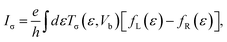 | (5) |
where
e is the electron charge,
h the Plank's constant, and
fL/R(
ε) is the distribution functions of the electrons in the left (right) electrode. Thus the current under bias was obtained by integrating over the bias window between the electrochemical potential of the left/right electrode.
44
Results and discussion
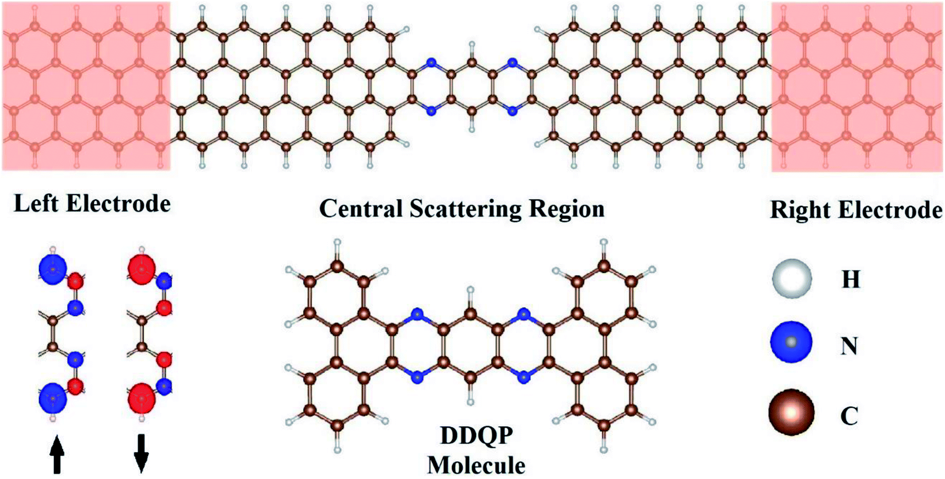
We designed our transport junction as shown in Fig. 1. The DDQP molecule is sandwiched in between two 4-ZGNR electrodes with ideal contacts, named ‘4D’. The number ‘4’ is the width of the ZGNR with four zigzag carbon chains according to the convention in the literature.45 We checked carefully the carbon–carbon bond lengths to be ranged 1.40–1.44 Å, slightly shorter at the edges and longer in the middle of the ZGNR. The carbon–nitrogen bond length is 1.36 Å near the DDQP center and 1.33 Å near the ZGNR electrodes. Sufficient periods of ZGNR are added into the central scattering region as buffer layers.
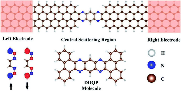 |
| | Fig. 1 A schematic illustration of the two-probe molecular device consisting dibenzo[a,c]dibenzo[5,6:7,8]quinoxalino[2,3-i]phenazine (DDQP) and two semi-infinite zigzag edged graphene nanoribbon (ZGNR) electrodes. The brown, blue, and gray spheres are carbon, nitrogen, and hydrogen, respectively. The spin density isosurfaces (0.002 e bohr −3) are shown for the ZGNR electrodes corresponding to different predefined magnetic configurations, in which blue and red colors represent density differences between up and down spin electrons. | |
As we know, different states of edge magnetic configuration15,16,45,46 may exist in the ZGNR, we specifically considered the ferromagnetic state across upper and lower edges of the electrodes, as shown in Fig. 1. These spin-polarized ZGNRs are known to be conductive, and we can set up two cases for the magnetic moments across the left and right electrodes, namely parallel (P) and anti-parallel (AP) configurations with equal and opposite magnetizations respectively.
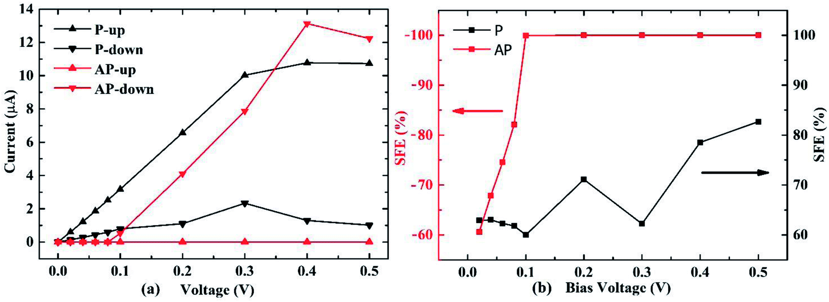
The spin resolved current (I) as a function of applied bias voltage (V) was calculated in the bias range from 0 V to 0.5 V, as shown in Fig. 2(a). In the P configuration, both up and down spin I–V curves show very good linear characteristics under small voltage. The I–V curves of P and AP configurations allow us to calculate the spin filter efficiency (SFE) which is defined as:
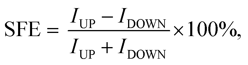
| | 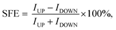 | (6) |
where
IUP and
IDOWN represent the current values of up and down spin electrons. The P case which has parallel spin configurations at both edges, gives SFE reaching 80% at 0.5 V. This giant value is much higher and more stable than that of
n-acene–graphene device.
47 For the AP case in which left and right electrodes have the antiparallel spins on both edges, a 100% SFE can be achieved such that the junction allows only one spin current passes through one direction, and the other spin through the opposite direction. These AP symmetry configurations of ZGNRs could result in extreme values of magnetoresistance ratio (MR) and highly spin-polarized currents.
16,48 However we note that the absolute values of the SFE and spin current of P are higher than AP configuration under low bias voltage.
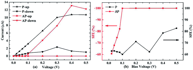 |
| | Fig. 2 (a) Spin-resolved current–voltage curves of the DDQP molecular spintronic device with 4-ZGNR electrodes for P and AP configurations; (b) spin filter efficiency (SFE) of P and AP magnetic configurations. Note that the down-spin current is larger in the AP system, and thus the SFE of AP has inverse sign in comparison with the P case. | |
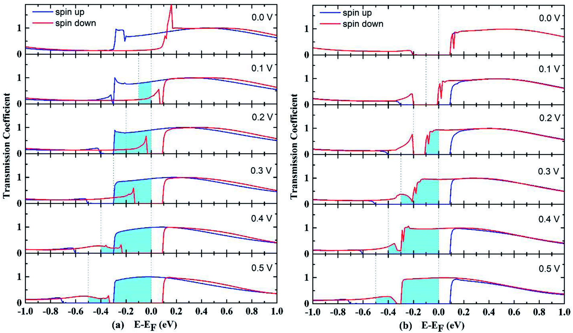
The transmission spectrum with bias window for P and AP spin configurations are shown in Fig. 3. The integrated area of light blue region equals the spin polarized electric current. In the P case as shown in Fig. 3(a), a gap-opening of the down spin transmission appears upon the bias voltage applied, and the transmission spectrum below Fermi level shifts to more negative energy range by the bias voltage. For AP configuration shown in Fig. 3(b), the transmissions at zero voltage for up and down spins both have a gap at Fermi level, and are almost overlapping each other. But with the increase of bias voltage, they show different behaviors so that the gap of up spin becomes larger while the gap of down spin closes up, resulting the domination of down spin in the whole bias window. In other words, the AP junction only allows one type of spin transport. The evolution of spin-resolved transmission spectra within the bias window is fully consistent with our results of SFE in Fig. 2(b) (spin resolved local density of states (LDOS) can be found at Fig. S1†).
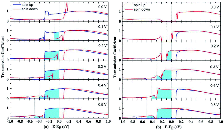 |
| | Fig. 3 Transmission coefficients under different bias voltages for (a) P and (b) AP spin configurations of the DDQP junction. The integration windows for obtaining I–V curves are shown by vertical lines and shaded areas in the transmission spectra. | |
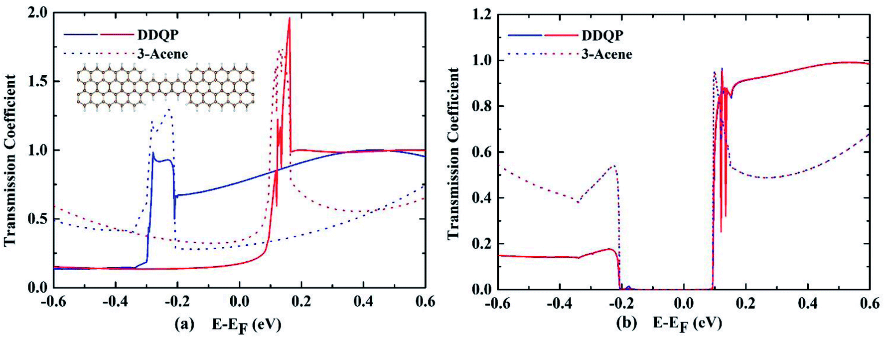
A deeper understanding of the origin of the high SFE is important to guide us to design devices with better performance. The transmission coefficients are shown in the Fig. 4, for comparison of a 3-acene and a DDQP molecule with P and AP spin configurations. It turns out that in the P configuration, two devices considered here are both metallic, whereas they both have a semiconducting band gap for the AP configuration. It is very interesting to see around the Fermi level that the 3-acene has up and down spin transmission of similar amplitudes, but for the DDQP the majority up spin electron's transmission coefficient is much higher than the minority down spin. This could explain the much higher SFE of DDQP device compared to the n-acene device.47 In Fig. 4(b), both devices show the same band gap due to the ZGNR,16 and the transmission spectra show spin degeneracy in the whole energy region. Scattering states wavefunctions are shown in Fig. 5. It is clear that the minority spin scattering state is being almost totally reflected, while only up spin scattering state tunnels through. As for the 3-acene device, the transmission of down spin and up spin transmission could hardly be distinguished at the Fermi energy. This phenomena confirms the enhanced SFE of the DDQP device.
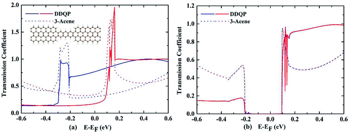 |
| | Fig. 4 Transmission coefficients at zero bias voltage for (a) the P configuration and (b) the AP configuration. The dashed lines represent the junction of 3-acene molecule (i.e. DDQP with nitrogen atoms substituted by hydrogenated carbon atoms) as shown in the inset of (a), and the solid lines are for the DDQP device. Blue and red colors denote up and down spin electron transmissions. | |
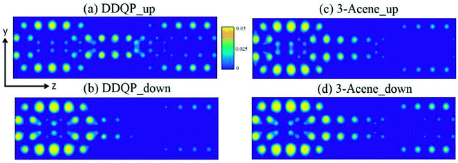 |
| | Fig. 5 Module square of real space scattering states of the DDQP device and 3-acene device at the Fermi energy EF and P spin configuration. (a) Up spin, (b) down spin of device with DDQP molecule; (c) up spin, (d) down spin of device based on 3-acene molecule. | |
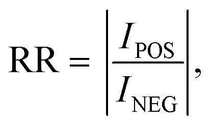
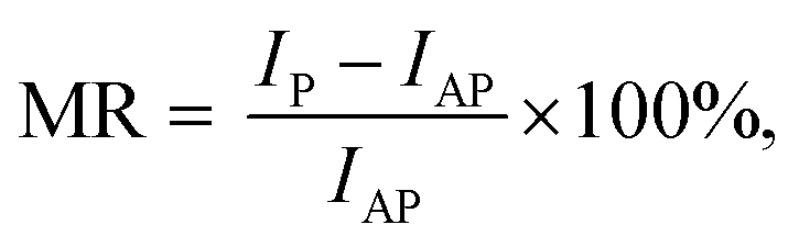
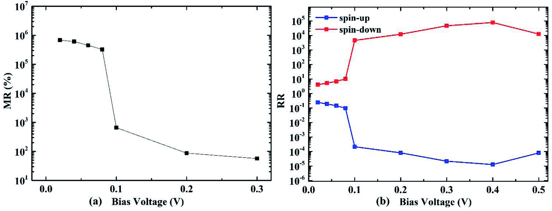
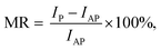
Rectifying ratio (RR) of the AP spin configuration is investigated as shown in Fig. 6(b). It is defined as:
| |  | (7) |
where
IPOS or
INEG is the current value of the transportation when the device is under positive (from lead 1 to lead 2) or negative (from lead 2 to lead 1) bias voltage. The RR curve shows a linear trend below 0.09 V, but boosts three orders of magnitude once the bias voltage reaches 0.1 V, then steadily goes up to 0.5 V. This linear change at low bias and the giant sudden change of the rectifying ratio may be useful for the spintronics application. Magnetoresistance ratio (MR) is shown in
Fig. 6(a), which is defined as:
| |  | (8) |
where
IP and
IAP correspond to the current value of P and AP configurations when they are under bias voltage. The MR of hydrogenated ZGNR electrode could be as high as to a magnitude of 10
6 at low bias voltage, then decrease rapidly as the bias voltage increases to 0.1 V. It's worth mentioning that the MR could reach a negative value when the bias voltage is further strengthened to 0.4 V or 0.5 V.
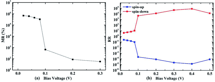 |
| | Fig. 6 (a) Magnetoresistance ratio (MR) and (b) rectifying ratio (RR) of the molecular transport device with 4-ZGNR electrodes, as functions of the bias voltage. | |
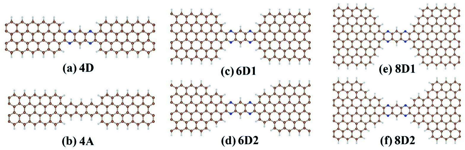
We considered DDQP device with 4/6/8-ZGNR electrode of different terminal geometry under P configuration as their center scattering region as shown in Fig. 7(a)–(f). Taken “6D1” as an example, the first number “6” means that this junction is linked by 6-ZGNR at both ends as electrodes; “D” and “A” distinguish whether the central part is DDQP or 3-acene; the number “1” or “2” is for DDQP junctions having the same width of electrode but different particular edge geometries.
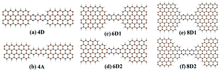 |
| | Fig. 7 Classification of all the structures calculated with different ZGNR-DDQP connection geometries, and ZGNR width of 4 for (a) and (b), 6 for (c) and (d), 8 for (e) and (f). | |
I–V characteristic and SFE of the above mentioned structures are all shown in Fig. 8. For all the ZGNR electrodes with different width, their total current curves show good linearity, which is different from normal double edge N-doped ZGNR.49 For the P spin configuration which is simpler than AP, the SFE seems hard to be lifted through general method of prolonging the center molecule.47 But in DDQP devices, it's clear according to Fig. 8(b) that SFE could be increased up to near 100% just with the ZGNR width extending from 4 to 8, while we note differences between 6D1 and 6D2, 8D1 and 8D2 are not negligible(see details at Fig. S2 and S3†). We can see that the narrow ZGNR electrodes lead to higher total conductance, and lower SFE; compared with smooth edged device like 6D1 or 8D1, carbon atom vacancies located at the transition region between electrode and scattering region will increase both the total conductance and SFE. The lower current value of devices with wider ZGNR electrodes is due to the longer tunnelling length of electrons between center molecule and edges of ZGNR, as the main channel of transporting electrons. And the higher conductance and SFE of 6D2 than 6D1, 8D2 than 8D1 relate closely to the declining zigzag edges which block electrons with non-parallel momentum, since fragmented edges with narrower potential barrier width will enhance the tunnelling (see details at Fig. S4†).
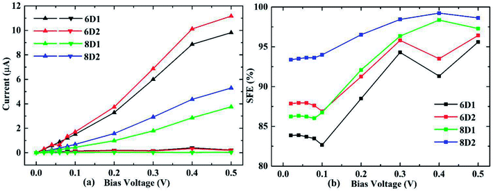 |
| | Fig. 8 (a) Current–voltage curves for different structures discussed in the text under P spin configuration, the up pointed triangles correspond to up spin I–V curves, and the downward ones to down spin; (b) SFE of different electrode width and terminal structure configurations. | |
Conclusions
In summary, electron transport computation was performed for molecular spintronic devices based on a single DDQP molecule with ZGNR electrodes, by combining real space self-consistent density functional theory and the Keldysh non-equilibrium Green's function formalism. We investigated the spin polarized current–voltage characteristics, giant spin filter efficiency, magnetoresistance and rectification ratio. Significant enhancement of performance was obtained when comparing with the analogue 3-acene molecule device. Good controls of such polycyclic aromatic molecules with different structures in mesoscopic devices are becoming feasible with the experimental synthesis advancements.50,51 To better design and understand molecular spintronic device, we studied the effect of ZGNR electrode width dependence and molecule–electrode connection geometries, which could help us further improve the SFE toward 100% under low bias voltage and simple parallel spin configuration. Similar methodology can also be applied to investigate the effects of non-planar configuration52 or ZGNR edge modification (for example, see Fig. S5†). We expect that this work will be beneficial for basic electron transport researches on precise atomistic control and spin injection in molecular spintronics.
Conflicts of interest
There are no conflicts to declare.
Acknowledgements
This research was supported by the National Key Basic Research Program of China (Grant No. 2015CB921600), the National Natural Science Foundation of China (Grant No. 51861145315, No. 11547011, and No. 51672171), and the Eastern Scholar Program from the Shanghai Municipal Education Commission. The Special Program for Applied Research on Super Computation of the NSFC–Guangdong Joint Fund (the second phase) under Grant No. U1501501, the fund of the State Key Laboratory of Solidification Processing in NWPU (Grant No. SKLSP201703), the supercomputing services from AM-HPC, and Fok Ying Tung education foundation are also acknowledged. J. H. Z. acknowledges the NSF from Science and Technology Department of Guizhou Province (no. QKJC [2016]1113, QHPT [2017]5790-02). G. D. Z. thank, Lufeng Ruan, Junjun Li and Wenze Xie for their useful discussions on the use of Nanodcal software.
Notes and references
- X. Cui, A. Primak, X. Zarate, J. Tomfohr, O. Sankey, A. Moore, T. Moore, D. Gust, G. Harris and S. Lindsay, Science, 2001, 294, 571–574 CrossRef CAS PubMed.
- H. B. Akkerman, P. W. Blom, D. M. De Leeuw and B. De Boer, Nature, 2006, 441, 69 CrossRef CAS PubMed.
- J. Lee, H. Chang, S. Kim, G. S. Bang and H. Lee, Angew. Chem., 2009, 121, 8653–8656 CrossRef.
- E. Lortscher, Nat. Nanotechnol., 2013, 8, 381–384 CrossRef PubMed.
- X. Guo, J. P. Small, J. E. Klare, Y. Wang, M. S. Purewal, I. W. Tam, B. H. Hong, R. Caldwell, L. Huang and S. O'brien, Science, 2006, 311, 356–359 CrossRef CAS PubMed.
- C. W. Marquardt, S. Grunder, A. Baszczyk, S. Dehm, F. Hennrich, H. v. Löhneysen, M. Mayor and R. Krupke, Nat. Nanotechnol., 2010, 5, 863–867 CrossRef CAS PubMed.
- W. Ren, J. R. Reimers, N. S. Hush, Y. Zhu, J. Wang and H. Guo, J. Phys. Chem. C, 2007, 111, 3700–3704 CrossRef CAS.
- F. Prins, A. Barreiro, J. W. Ruitenberg, J. S. Seldenthuis, N. Aliaga-Alcalde, L. M. Vandersypen and H. S. van der Zant, Nano Lett., 2011, 11, 4607–4611 CrossRef CAS PubMed.
- Y. Cao, S. Dong, S. Liu, Z. Liu and X. Guo, Angew. Chem., Int. Ed., 2013, 52, 3906–3910 CrossRef CAS PubMed.
- Q. Xu, G. Scuri, C. Mathewson, P. Kim, C. Nuckolls and D. Bouilly, Nano Lett., 2017, 17, 5335–5341 CrossRef CAS PubMed.
- K. S. Novoselov, A. K. Geim, S. V. Morozov, D. Jiang, Y. Zhang, S. V. Dubonos, I. V. Grigorieva and A. A. Firsov, Science, 2004, 306, 666–669 CrossRef CAS PubMed.
- M. J. Allen, V. C. Tung and R. B. Kaner, Chem. Rev., 2009, 110, 132–145 CrossRef PubMed.
- F. Perrozzi, S. Prezioso and L. Ottaviano, J. Phys.: Condens. Matter, 2015, 27, 013002 CrossRef CAS PubMed.
- S. Prezioso, F. Perrozzi, L. Giancaterini, C. Cantalini, E. Treossi, V. Palermo, M. Nardone, S. Santucci and L. Ottaviano, J. Phys. Chem. C, 2013, 117, 10683–10690 CrossRef CAS.
- Y. W. Son, M. L. Cohen and S. G. Louie, Nature, 2006, 444, 347–349 CrossRef CAS PubMed.
- W. Y. Kim and K. S. Kim, Nat. Nanotechnol., 2008, 3, 408–412 CrossRef CAS PubMed.
- M. Slota, A. Keerthi, W. K. Myers, E. Tretyakov, M. Baumgarten, A. Ardavan, H. Sadeghi, C. J. Lambert, A. Narita and K. Müllen, Nature, 2018, 557, 691 CrossRef CAS PubMed.
- H. Wan, B. Zhou, W. Liao and G. Zhou, J. Chem. Phys., 2013, 138, 034705 CrossRef PubMed.
- H. Wan, B. Zhou, X. Chen, C. Q. Sun and G. Zhou, J. Phys. Chem. C, 2012, 116, 2570–2574 CrossRef CAS.
- W. Liu, X. Luo, Y. Bao, Y. P. Liu, G. H. Ning, I. Abdelwahab, L. Li, C. T. Nai, Z. G. Hu, D. Zhao, B. Liu, S. Y. Quek and K. P. Loh, Nat. Chem., 2017, 9, 563–570 CrossRef CAS PubMed.
- W. Liu and K. P. Loh, Acc. Chem. Res., 2017, 50, 522–526 CrossRef CAS PubMed.
- S. Niimura, T. Fujimori, D. Minami, Y. Hattori, L. Abrams, D. Corbin, K. Hata and K. Kaneko, J. Am. Chem. Soc., 2012, 134, 18483–18486 CrossRef CAS PubMed.
- X. Zhu, C. Tian, C. L. Do-Thanh and S. Dai, ChemSusChem, 2017, 10, 3304–3316 CrossRef CAS PubMed.
- C. J. Burrows, Acc. Chem. Res., 2017, 50, 445 CrossRef CAS PubMed.
- B. Biel, X. Blase, F. Triozon and S. Roche, Phys. Rev. Lett., 2009, 102, 096803 CrossRef PubMed.
- S. Yu, W. Zheng, Q. Wen and Q. Jiang, Carbon, 2008, 46, 537–543 CrossRef CAS.
- S. Dutta, A. K. Manna and S. K. Pati, Phys. Rev. Lett., 2009, 102, 096601 CrossRef PubMed.
- Z. Chen, Y.-M. Lin, M. J. Rooks and P. Avouris, Phys. E, 2007, 40, 228–232 CrossRef CAS.
- M. Y. Han, B. Özyilmaz, Y. Zhang and P. Kim, Phys. Rev. Lett., 2007, 98, 206805 CrossRef PubMed.
- F. Sols, F. Guinea and A. H. C. Neto, Phys. Rev. Lett., 2007, 99, 166803 CrossRef CAS PubMed.
- M. Wimmer, I. Adagideli, S. Berber, D. Tomanek and K. Richter, Phys. Rev. Lett., 2008, 100, 177207 CrossRef PubMed.
- A. Saraiva-Souza, M. Smeu, H. Terrones, A. G. Souza Filho and M. A. Ratner, J. Phys. Chem. C, 2013, 117, 21178–21185 CrossRef CAS.
- Z. Li, H. Qian, J. Wu, B. L. Gu and W. Duan, Phys. Rev. Lett., 2008, 100, 206802 CrossRef PubMed.
- J. P. Perdew, K. Burke and M. Ernzerhof, Phys. Rev. Lett., 1996, 77, 3865 CrossRef CAS PubMed.
- P. E. Blöchl, Phys. Rev. B, 1994, 50, 17953 CrossRef PubMed.
- G. Kresse and J. Furthmüller, Phys. Rev. B, 1996, 54, 11169 CrossRef CAS PubMed.
- G. Kresse and D. Joubert, Phys. Rev. B, 1999, 59, 1758 CrossRef CAS.
- K. Momma and F. Izumi, J. Appl. Crystallogr., 2011, 44, 1272–1276 CrossRef CAS.
- J. Taylor, H. Guo and J. Wang, Phys. Rev. B, 2001, 63, 245407 CrossRef.
- D. Waldron, P. Haney, B. Larade, A. MacDonald and H. Guo, Phys. Rev. Lett., 2006, 96, 166804 CrossRef PubMed.
- J. P. Perdew and A. Zunger, Phys. Rev. B, 1981, 23, 5048 CrossRef CAS.
- D. Hamann, M. Schlüter and C. Chiang, Phys. Rev. Lett., 1979, 43, 1494 CrossRef CAS.
- W. Ren and J. Wang, Phys. Rev. B, 2004, 69, 033306 CrossRef.
- B. Wang, Y. Zhu, W. Ren, J. Wang and H. Guo, Phys. Rev. B, 2007, 75, 235415 CrossRef.
- Y. W. Son, M. L. Cohen and S. G. Louie, Phys. Rev. Lett., 2006, 97, 216803 CrossRef PubMed.
- M. Fujita, K. Wakabayashi, K. Nakada and K. Kusakabe, J. Phys. Soc. Jpn., 1996, 65, 1920–1923 CrossRef CAS.
- D. Zou, B. Cui, X. Kong, W. Zhao, J. Zhao and D. Liu, Phys. Chem. Chem. Phys., 2015, 17, 11292–11300 RSC.
- R. Qin, J. Lu, L. Lai, J. Zhou, H. Li, Q. Liu, G. Luo, L. Zhao, Z. Gao, W. N. Mei and G. Li, Phys. Rev. B, 2010, 81, 233403 CrossRef.
- L. Liu, X.-F. Li, Q. Yan, Q.-K. Li, X.-H. Zhang, M. Deng, Q. Qiu and Y. Luo, Phys. Chem. Chem. Phys., 2017, 19, 44–48 RSC.
- W. Lu and C. M. Lieber, Nat. Mater., 2007, 6, 841 CrossRef CAS PubMed.
- D. Xiang, X. Wang, C. Jia, T. Lee and X. Guo, Chem. Rev., 2016, 116, 4318–4440 CrossRef CAS PubMed.
- J. Li, L. Ruan, Z. Wu, G. Zhang and Y. Wang, Phys. Chem. Chem. Phys., 2018, 20, 7167–7172 RSC.
Footnote |
| † Electronic supplementary information (ESI) available. See DOI: 10.1039/c8ra07343k |
|
| This journal is © The Royal Society of Chemistry 2018 |
Click here to see how this site uses Cookies. View our privacy policy here. 
 Open Access Article
 This Open Access Article is licensed under a Creative Commons Attribution-Non Commercial 3.0 Unported Licence
 ab,
Li-Meng
Li
ab,
Yin
Wang
ab,
Li-Meng
Li
ab,
Yin
Wang