
 Open Access Article
 This Open Access Article is licensed under a Creative Commons Attribution-Non Commercial 3.0 Unported Licence
Direct laser-patterned ultra-wideband antennae with carbon nanotubes
Haochuan Qiuab,
Houfang Liu*ab,
Xiufeng Jiaab,
Xiao Liuab,
Yuxing Liab,
Jiafeng Fengc,
Hongxiang Weic,
Yi Yangab and
Tian-ling Ren *ab
*ab
aInstitute of Microelectronics, Tsinghua University, Beijing 100084, China. E-mail: hfliu@tsinghua.edu.cn; RenTL@tsinghua.edu.cn
bTsinghua National Laboratory for Information Science and Technology, Tsinghua University, Beijing 100084, China
cBeijing National Laboratory of Condensed Matter Physics, Institute of Physics, University of Chinese Academy of Science, Chinese Academy of Sciences, Beijing 100190, China
First published on 5th September 2018
Abstract
Ultra-wideband (UWB), a radio transmission technology with wide bandwidth exceeding the minimum of 500 MHz or at least 20% of the center frequency, is a revolutionary approach for short-range high-bandwidth wireless communication. In this study, carbon nanotube (CNT) UWB antennas by direct laser-patterning technology have been successfully designed, fabricated and characterized. In contrast with traditional fabrication methods, the direct laser-patterning technology offers an exceptional potential for custom-designed, high-complexity and accuracy device fabrication. The “engraving” process on CNTs exposed to laser can be attributed to the bond breaking of C–C, evaporation of carbon atoms, and oxidation of CNTs by the oxygen molecules. Numerical analysis and experimental studies provide characteristics of CNT slot antennas with a wide impedance bandwidth (from 3.4 GHz to 14 GHz for S11 ≤ −10 dB), high average radiation efficiency (76%) and fractional bandwidth (121%) with small size of 30 × 30 mm2. The results indicate the advantages of laser-patterned UWB antennas based on carbon nanotubes, which paves the way for industrial applications, particularly in the world of consumer electronics.
Introduction
The next-generation of portable, flexible, and wearable electronics devices, especially in the growing Internet of Things (IoT), demands wireless data transmission with lower power consumption and higher data propagation speed.1–4 The use of ultra-wideband (UWB),5 which can occupy an extremely wide bandwidth exceeding the minimum of 500 MHz or at least 20% of the center frequency and very short pulses, has been considered as a revolutionary solution to employ low transmission power, avoid multipath fading and provide a high data transfer rate. Therefore, high performance UWB antennas for communication systems are the focus of science and technology nowadays. Since their discovery in 1991, carbon nanotubes (CNTs) have been considered as promising materials for CMOS field-effect transistors,6 nonvolatile random access memory,7 thin-film transistors for OLEDs8 and RF antennas,9 due to their good biocompatibility, high stability, and excellent electrical and mechanical properties.In recent years, numerous methods have been proposed for CNT antennas, such as printing,10 cutting operation11 and injecting CNT ink into slots.12 As reported in ref. 13, CNTs were printed on both sides of the substrate and then cut by milling machine to obtain a multiband antenna. The CNT material had to be hardened by resin infiltration before processed on the milling machine.13 However, this approach was complex and expensive. Recently, a CNT sheet patch antenna was reported with the CNT sheet laminated on the Teflon substrate or transferred to Kapton tape.14 Nevertheless, these methods are not very suitable for cost-effective and high-accuracy micro-scale fabrication of UWB slot antennas, which require smaller size and more stable performance. Utilizing CNT as conductor for antennas in microwave region is still challenging due to the limited fabrication technology. In this paper, a custom-designed, transfer-free, high-accuracy method for the fabrication of UWB antenna based on CNTs will be demonstrated, which is electrically characterized and simulated by Vector Network Spectrum Analyzer (VNA), Advanced Design System (ADS) and Ansoft HFSS (High-frequency Simulation Structure), respectively. The proposed antennas are fabricated by one-step laser-patterned method on quartz substrate with ξr = 3.78 and thickness d = 1.5 mm and fed by CPW lines. The validated excellent performance of the prototype UWB antennas operating from 3.4 to 14 GHz indicates that the one-step laser-patterned CNTs antennas present a novel pathway towards customized IoT communication technology.
Experimental section
Sample preparation
The CNT films on quartz substrate were prepared by the droplets of metallic CNT water solution with diameters of 1.2–1.7 nm and length varies from 300 nm to 5 μm (Nanjing XFNANO Materials TECH Co., Ltd in China.). And then, the samples were dried at 80 °C for 15 min. Finally, the samples with CNT film were fabricated on the homemade automatic patterning platform with different laser power, such as 0.5 W, 1 W, 1.5 W and 2 W. The laser-patterning platform composes of one laser with wavelength of 450 nm, and a controlling PC. Using the homemade design software, the designed structure was transferred to the CNT film by the laser-induced oxidation of CNT film.Characterization
The SEM (scanning electron microscope) image of CNT film was observed using Raith e-line plus SEM. The Raman spectroscopy was obtained using Horiba Jobin Yvon LabRAM HR-Evolution. The return loss was measured with an Agilent PNA-X series N5242A network analyzer, and the radiation patterns were obtained in an anechoic chamber. The real-time temperature of the CNT film exposed to the laser was measured using an infrared thermal imager (FLUKE, TI 200).Results and discussions
CNTs have emerged as good candidates for lightweight, durable UWB antennas, due to their unique physical and electrical properties, such as corrosion resistance, weight savings, reliability and enhanced electrical characteristics. Although CNTs can be manufactured using several printing and transferring techniques,15–17 continuous improvements of fabrication process in unique design, scalability and high-accuracy are required to realize their advantages. Fig. 1a illustrates the laser-patterning process for CNT-based UWB antennas on quartz substrates. (The detailed process is described in the Experimental Section.) The laser-patterning process can selectively engrave the CNTs where not desired to leave a pattern. The series of patterning laser power have been optimized such as 0.5 W, 1 W, 1.5 W and 2 W, as shown in Fig. 1b. In case of lower laser power, 0.5 W, 1 W and 1.5 W for example, there are still some remaining of CNTs in the engraved area. When the laser power is up to 2 W, there is no remaining left. Considering the remaining of the CNTs may introduce parasitic parameters and degrade the performance the antenna, we chose the laser power of 2 W. Fig. 1c shows the Raman spectra of the CNTs on the quartz substrate. The three dominant Raman features are clearly investigated, the radial breathing mode (RBM) at low frequencies, the disorder-induced D band and the tangential G band multi-feature at higher frequencies, which are in agreement with previous works.18–20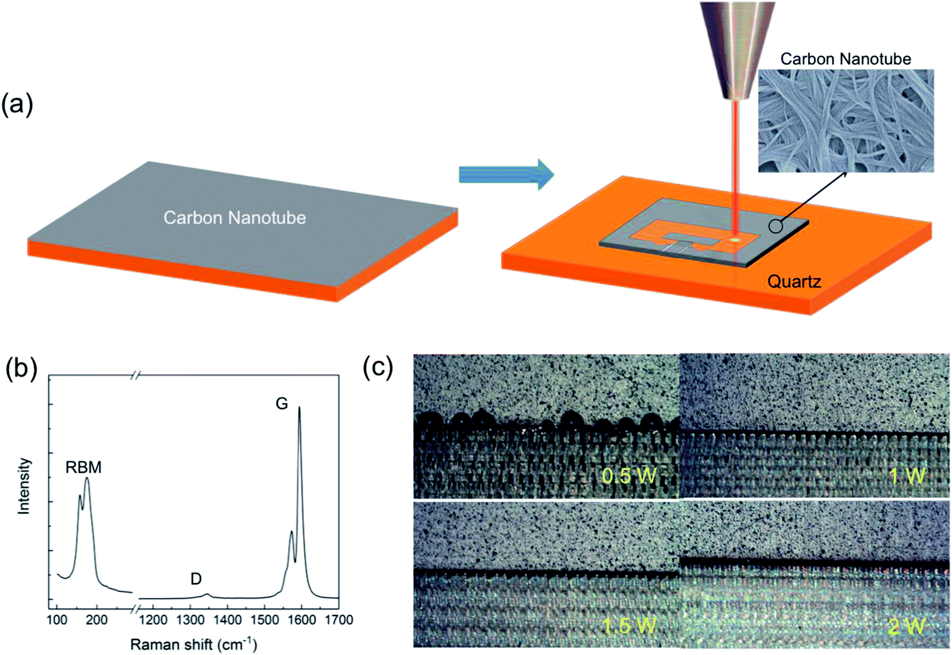 | ||
| Fig. 1 (a) Schematic of the laser pattering processes, the inset shows the SEM images of the CNTs. (b) Raman spectra of the CNTs. The characteristic peaks, RBM, G, and D, are clearly visible. (c) Optimized fabrication process on CNT films by the homemade automatic patterning platform with different laser power, such as 0.5 W, 1 W, 1.5 W and 2 W. | ||
To study the oxidation process of CNT engraved by the laser, a simulation model was established using multi-physical field and finite element analyzing method. As an important parameter of laser patterning process, the overlapping rate (Of) is defined as 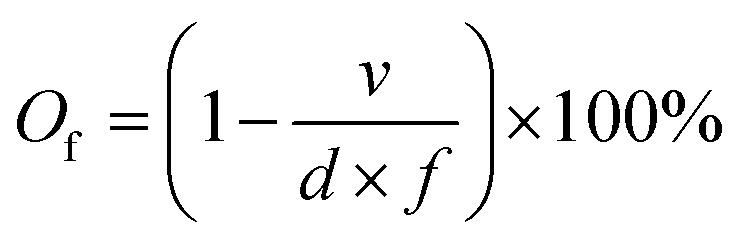 , where d is the focused beam diameter, v is the laser scanning speed, and f is the laser repetition rate.21,22 A 5 μm-thick CNT slice is placed on the quartz substrate. The laser absorption of the CNT is simplified, ignoring the optical enhance by the complex structure of CNT. The laser moves upon the CNTs at a constant speed v with Gaussian power distribution:23
 | (1) |
 | (2) |
![[thin space (1/6-em)]](https://www.rsc.org/images/entities/char_2009.gif) J (kg K)−1, kCNT = 40 W (m K)−1 and kQuartz = 1.4 W (m K)−1. The simulation results under different laser power are shown in Fig. 2a. The temperature distribution consists of a group of eccentric circles during the movement of the laser, where the central bright area represents the irradiated region. The sharp temperature distribution can be attributed to the strong heating effect and heat dissipation among CNTs, substrate and air. Note that the temperature distribution generated by the moving laser irradiation on CNTs has a “tailed” phenomenon including two blended areas: an irradiation area and scanning-induced area as a result of the moving laser beam. This tail effect also reflects the thermal conductivity and the material surface area. The brightness, size and the contrast variations of the irradiated spots in the infrared images confirm the increase of the laser-generated temperatures as the laser power increases. It is evident that the higher laser power results in the higher generated temperature. The maximum temperature of the CNTs at laser power of 2 W can reach up to 557 °C. The higher irradiation temperature can not only induce the bond breaking of C–C and evaporation of carbon atoms, but also cause the oxidation of CNTs from microstructures by the oxygen molecules in the air. These simulated results agree well with the experimental results, as shown in Fig. 2b. The real-time surface temperature of the CNT films was recorded by an infrared thermal imager (FLUKE, TI 200).
J (kg K)−1, kCNT = 40 W (m K)−1 and kQuartz = 1.4 W (m K)−1. The simulation results under different laser power are shown in Fig. 2a. The temperature distribution consists of a group of eccentric circles during the movement of the laser, where the central bright area represents the irradiated region. The sharp temperature distribution can be attributed to the strong heating effect and heat dissipation among CNTs, substrate and air. Note that the temperature distribution generated by the moving laser irradiation on CNTs has a “tailed” phenomenon including two blended areas: an irradiation area and scanning-induced area as a result of the moving laser beam. This tail effect also reflects the thermal conductivity and the material surface area. The brightness, size and the contrast variations of the irradiated spots in the infrared images confirm the increase of the laser-generated temperatures as the laser power increases. It is evident that the higher laser power results in the higher generated temperature. The maximum temperature of the CNTs at laser power of 2 W can reach up to 557 °C. The higher irradiation temperature can not only induce the bond breaking of C–C and evaporation of carbon atoms, but also cause the oxidation of CNTs from microstructures by the oxygen molecules in the air. These simulated results agree well with the experimental results, as shown in Fig. 2b. The real-time surface temperature of the CNT films was recorded by an infrared thermal imager (FLUKE, TI 200).
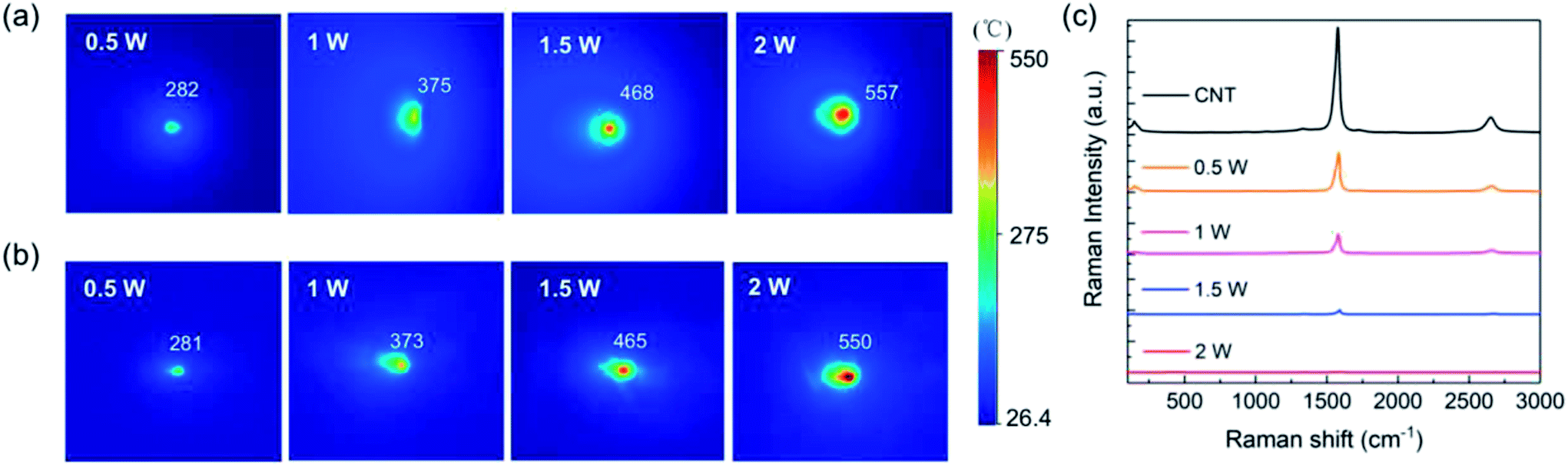 | ||
| Fig. 2 (a) Simulated and (b) experimental infrared images of the CNT films during engraving process with different laser powers of 0.5 W, 1 W, 1.5 W and 2 W, respectively. (c) Raman spectra of the CNT films exposed to the laser with different laser powers of 0 W, 0.5 W, 1 W, 1.5 W and 2 W, respectively. | ||
In general, the intensity of G-band peak around 1580 cm−1, which is associated to C–C stretching vibrations, can be used to reflect the amount of probed material and the efficiency of the Raman scattering process, including morphological constraints.25 The Raman spectra of the CNT films are shown in Fig. 2c, which are exposed to the laser with different power of 0 W, 0.5 W, 1 W, 1.5 W and 2 W, respectively. The density of G-band peak decreases with the increment of the laser power. As the laser power is up to 2 W, the density almost falls to zero, indicating that the CNT film is completely removed from the substrate.
For UWB antenna, the microstrip slot design is recommended as its relative small size, cost-effective, and easier to be integrated which are important in UWB applications.26,27 Therefore, considering the relative higher resistivity compared with metal, by properly choosing the dimension parameters of the wide slot and radiating patch, we propose a geometry structure of the slot antenna. Fig. 3a and b show the optical image and concrete parameters of the rectangular slot antenna, which consists of corners beveled patch and a ground plane etched with two semicircle slots with radius of 1 mm. The CPW feed line has a center strip width of 3.5 mm and a gap distance of gap = 0.6 mm between the signal strip and the finite coplanar rectangular ground plane.
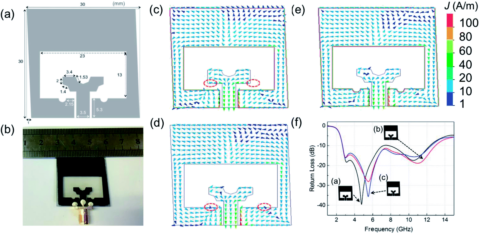 | ||
| Fig. 3 Geometry (a) and photo (b) of the proposed slot antenna (unit: millimeters). (c) Surface current distributions at 5 GHz of three designed UWB slot antennas with simple Y shaped patch, (d) beveled Y shaped patch, and (e) beveled rectangular patch and two semicircle slots in the ground plane; (f) simulated return losses |S11| of these three designed antennas. | ||
ADS and Ansoft HFSS, which are based on the finite element method, are used to design and optimize the design structure of slot antennas. In simulations, the conductivity of the CNT is provided as σ = 1/(tRsquare) = 5 × 10⁴ s m−1, where t = 5 μm is the thickness of the CNT films measured with SEM, Rsquare = 4 Ω is the surface resistance measured by four probe method. For better low-frequency impedance matching specified by the electrical length of current, the rectangular slot in the ground plane providing a long current path is designed. To obtain good impedance characteristics at middle frequency, two octagon notches which can create balance between the vertical and horizontal electrical currents are also applied to both sides of the Y shaped radiating patch, hence additional resonances have been realized and finally the total bandwidth of the antenna broadened. Finally, two semicircle slots with a radius of 1 mm are etched at the both sides of the CPW feedline on the ground plane to further improve the performance at middle frequency. Better coupling between the lower edges of the radiating patch and the ground plane can be obtained by suitably choosing the radius and position of the semicircle slots. Fig. 3c–f shows the surface current distribution at 5.4 GHz of three designed UWB slot antennas with (a) simple Y shaped patch, (b) beveled Y shaped patch, and (c) beveled rectangular patch and two semicircle slots at the ground plane. The discontinuity and irregular of surface currents appear at both corners and the ground plane's edges opposite to the lower edge of the radiating patch, as marked with red circles in Fig. 3c and d, respectively. After these parts removed by laser patterning, the additional resonances and better impedance matching are obtained.
As an important aspect of antenna characterization, the return loss |S11| indicates the input power acceptance level of the antenna.28 The simulated return losses (|S11|) of the antenna are shown in Fig. 3f. Compared with the design structures (a) and (b), there is wider bandwidth and better impedance matching in wider frequency range for the design structure (c) with beveling the corners of the Y shaped radiating patch and inserting semi-circles on both sides of the ground plan. The simulated and measured return losses (|S11|) of the slot antenna with structure (c) are shown in Fig. 4b, where a reasonable agreement between simulation and measurement is observed. Importantly, the frequency band for |S11| > 10 dB is from 3.4 GHz to 14 GHz, which is well matched within the UWB bandwidth from 3.1 to 10.6 GHz, that is, |S11| > 10 dB, indicating that more than 90% input power is transmitted in this band.29–31
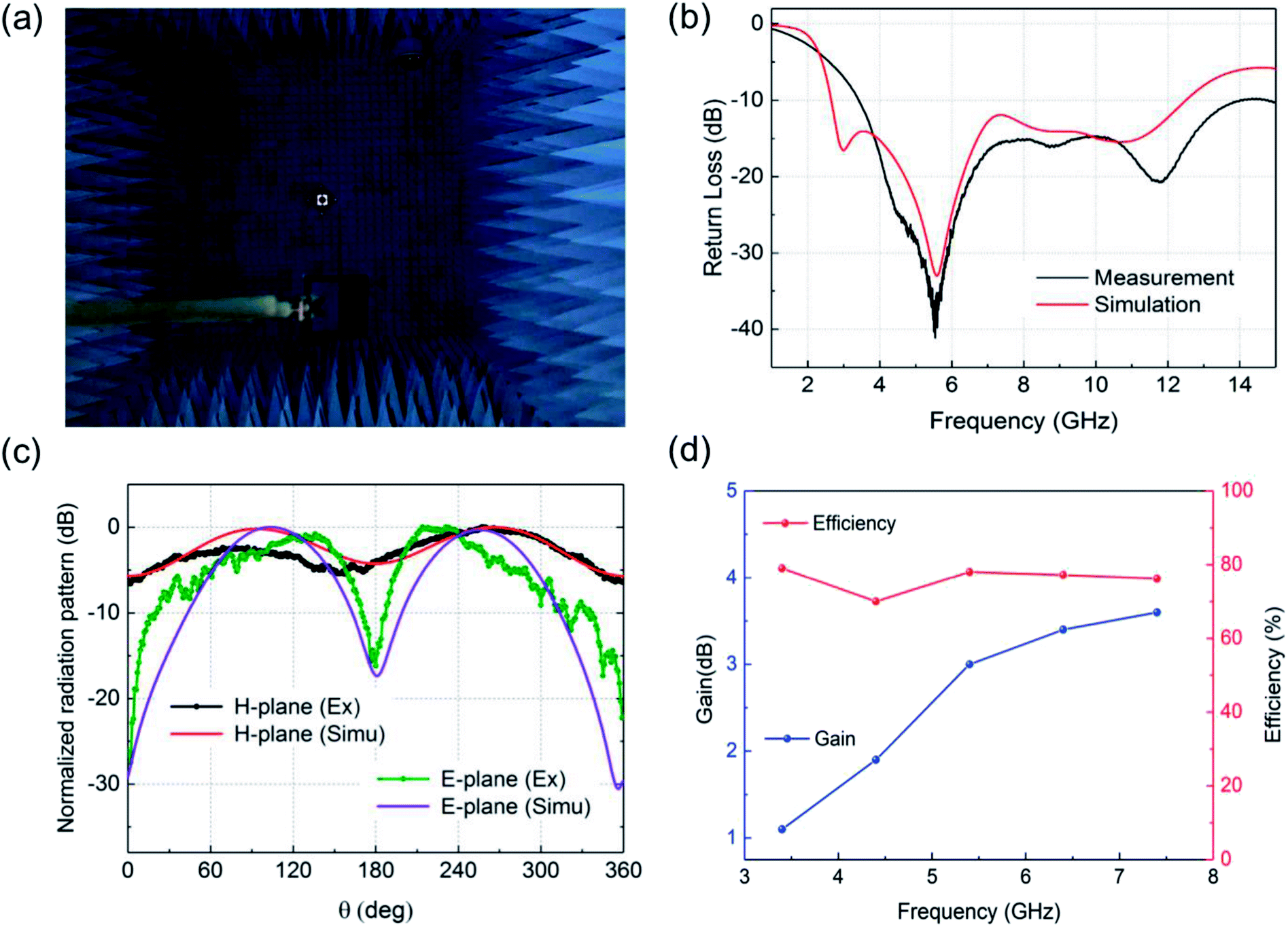 | ||
| Fig. 4 (a) Image of radiation pattern measurements in anechoic chamber. (b) Simulated and measured return losses |S11| of the slot antenna with beveled rectangular patch and two semicircle slots in the ground plane, and (c) the normalized radiation pattern in both E-(xz) and H-(yz) planes. (d) Measured gain and efficiency of the antenna as a function of frequency. | ||
To further verify the radiation, the normalized radiation pattern of the CNT antennas in both E-(xz) and H-(yz) planes were measured as shown in Fig. 4c. The CNT antenna under test and the reference-radiating antenna are connected with the VNA. The CNT antenna is placed on the turn table as a receiver and the standard reference antenna is fastened on the stand as a radiator. The data were recorded for every 1° rotation.32 For brevity, the normalized radiation patterns at 6.4 GHz are reported and there is good agreement between simulation and measurements. It is observed that the CNT UWB antenna shows a stable radiation pattern over the frequency range. The radiation pattern is found to be almost omnidirectional in the H-plane, which is of most interest for wireless communication systems, and nearly monopole-like radiation pattern in the E-plane as expected.
To further investigate the performance of the antenna, the fractional bandwidth (FBW) of the antenna can be defined as, which is also expressed as percent bandwidth:33
| FBW = (f2 − f1)/f0 = 2(f2 − f1)/(f2 + f1) | (3) |
| Reference | Fabrication | Dimension (mm2) | FBW (%) |
|---|---|---|---|
| Ref. 10 | Printing | 48 × 33 | 96% |
| Ref. 11 | MA | 50 × 50 | 34% |
| Ref. 12 | Injection | 20 × 18 | 12% |
| Ref. 34 | Transferring | 36 × 50 | 19% |
| Ref. 35 | MA | — | 11% |
| Ref. 36 | MA | 20 × 20 | 25% |
| Ref. 37 | Printing | 58 × 58 | 50% |
| Ref. 38 | Transferring | 30 × 30 | 4.5% |
| This work | Laser-patterning | 30 × 30 | 121% |
As a significant performance parameter of antennas, the radiation gain was measured in the anechoic chamber, as shown in Fig. 4a. The radiation efficiency (η) is the ratio of the total power radiated by the antenna to the power delivered to the input terminals. With maximum radiation as reference, the radiation efficiency can be calculated as η = gain/directivity, which indicates the conductor and dielectric losses due to the antenna materials.39 In Fig. 4d, the measured efficiency η has an averaged value of 76% over band range from 3.5 GHz to 7.5 GHz, which is one of the highest reported values for CNT antennas in the UWB applications up to date. The achievement of 76% efficiency is probably due to the good impedance matching and low ohmic loss of the CNTs antenna. These results also suggest that the antenna based on CNTs can achieve satisfactory performance with ultra-wide band, due to the high quality of CNT sheets, antenna design and one-step accurate laser-patterned method.
Conclusion
In summary, a custom-designed, mask-less, and high-accuracy fabrication method for robust and conductive CNT film using direct laser-patterning technology has been demonstrated for application in UWB microwave antenna design. The simulated and measured results show that the proposed CNT slot antenna possesses excellent performance with an ultrawide bandwidth performance between 3.4 GHz and 14 GHz, high average radiation efficiency of 76% and FBW as high as 121% with small size of 30 × 30 mm2. This work suggests that the laser-patterned CNT antennas hold the potential for high-volume applications in the microwave region.Conflicts of interest
The authors declare no competing financial interest.Acknowledgements
This work was supported by National Natural Science Foundation (61574083, 61434001, 11674373), National Key R&D Program (2016YFA0200400), National Basic Research Program (2015CB352101), Special Fund for Agroscientific Research in the Public Interest (201303107) of China, and Research Fund from Beijing Innovation Center for Future Chip. The authors are also thankful for the support of Open Research Fund Program of the State Key Laboratory of Low-Dimensional Quantum Physics (KF201715) and Independent Research Program (2014Z01006) of Tsinghua University. J. F. acknowledges Youth Innovation Promotion Association of Chinese Academy of Sciences (2017010).References
- I. F. Akyildiz and J. M. Jornet, IEEE Wirel. Commun., 2010, 17, 58–63 Search PubMed.
- L. Lizzi, F. Ferrero, P. Monin, C. Danchesi and S. Boudaud, IEEE 6th International Conference on Communications and Electronics (ICCE), 2016 Search PubMed.
- H. L. Zhu, B. Baby Narakathu, Z. Q. Fang, A. T. Aijazi, M. Joyce, M. Atashbarb and L. B. Hu, Nanoscale, 2014, 6, 9110 RSC.
- J. Kang, Y. Matsumoto, X. Li, J. K. Jiang, X. J. Xie, K. Kawamoto, M. Kenmoku, J. H. Chu, W. Liu, J. Mao, K. Ueno and K. Banerjee, Nature Electronics, 2018, 1, 46–51 CrossRef.
- T. K. K. Tsang and M. N. El-Gamal, The 3rd International IEEE - NEWCAS Conference, 2005, vol. 381–386, pp. 19–22 Search PubMed.
- C. G. Qiu, Z. Y. Zhang, M. M. Xiao, Y. J. Yang, D. L. Zhong and L.-M. Peng, Science, 2000, 355, 271–276 CrossRef PubMed.
- T. Rueckes, K. Kim, E. Joselevich, G. Y. Tseng, C.-L. Cheung and C. M. Lieber, Science, 2000, 289, 94–97 CrossRef PubMed.
- M. A. McCarthy, B. Liu, E. P. Donoghue, I. Kravchenko, D. Y. Kim, F. So and A. G. Rinzler, Science, 2011, 332, 570–573 CrossRef PubMed.
- E. A. Bengio, D. Senic, L. W. Taylor, D. E. Tsentalovich, P. Y. Chen, C. L. Holloway, A. Babakhani, C. J. Long, D. R. Novotny, J. C. Booth, N. D. Orloff and M. Pasquali, Appl. Phys. Lett., 2017, 111, 163109 CrossRef.
- Z. Hamouda, J.-L. Wojkiewicz, A. A. Pud, L. Kone, B. Belaabed, S. Bergheul and T. Lasri, IEEE Trans. Antennas Propag., 2015, 63, 5864–5867 Search PubMed.
- A. Mehdipour, I. D. Rosca, A.-R. Sebak, C. W. Trueman and S. V. Hoa, IEEE Trans. Antennas Propag., 2011, 59, 3572–3578 Search PubMed.
- I. Puchades, J. E. Rossi, C. D. Cress, E. Naglich and B. J. Landi, ACS Appl. Mater. Interfaces, 2016, 8, 20986–20992 CrossRef PubMed.
- A. Mehdipour, I. D. Rosca, A.-R. Sebak, C. W. Trueman, Senior Member and S. V. Hoa, IEEE Antennas Wirel. Propag. Lett., 2010, 9, 891–894 Search PubMed.
- S. D. Keller, A. I. Zaghloul, V. Shanov, M. J. Schulz, D. B. Mast and N. T. Alvarez, IEEE Trans. Antennas Propag., 2014, 62, 48–54 Search PubMed.
- W. Zeng, L. Shu, Q. Li, S. Chen, F. Wang and X.-M. Tao, Adv. Mater., 2014, 26, 5310–5336 CrossRef PubMed.
- W. Wu, Nanoscale, 2017, 9, 7342 RSC.
- M. A. Meitl, Y. X. Zhou, A. S. Gaur, S. Jeon, M. L. Usrey, M. S. Strano and J. A. Rogers, Nano Lett., 2004, 4, 1643–1647 CrossRef.
- A. M. Rao, E. Richter, S. Bandow, B. Chase, P. C. Eklund, * K. A. Williams, S. Fang, K. R. Subbaswamy, M. Menon, A. Thess, R. E. Smalley, G. Dresselhaus and M. S. Dresselhaus, Science, 1997, 275, 187–191 CrossRef PubMed.
- A. Hartschuh, H. N. Pedrosa, L. Novotny and T. D. Krauss, Science, 2003, 301, 1354–1356 CrossRef PubMed.
- M. S. Dresselhaus, A. Jorio, M. Hofmann, G. Dresselhaus and R. Saito, Nano Lett., 2010, 10, 751–758 CrossRef PubMed.
- H. K. Lin, R. C. Lin and C. H. Li, Thin Solid Films, 2010, 518, 7253–7257 CrossRef.
- J.-W. Yoon, W. S. Chang and S. H. Cho, Opt. Laser. Eng., 2015, 73, 40–45 CrossRef.
- R. Brockmann, K. Dickmann, P. Geshev and K. J. Matthes, Int. J. Heat Mass Transf., 2003, 46, 717–723 CrossRef.
- R. Uyhan, J. Appl. Math., 2013, 2013, 649590 CrossRef.
- J. R. Mialichi, M. J. S. P. Brasil, F. Iikawa, C. Veríssimo and S. A. Moshkalev, J. Appl. Phys., 2013, 114, 024904 CrossRef.
- S. Sadat, M. Fardis, F. Geran and G. Dadashzadeh, Prog. Electromagn. Res., 2007, 67, 173–179 CrossRef.
- T. T. Tung, S. J. Chen, C. Fumeaux and D. Losic, J. Mater. Chem. C, 2016, 4, 10620 RSC.
- A. M. Hussain, F. A. Ghaffar, S. I. Park, J. A. Rogers, A. Shamim and M. M. Hussain, Adv. Funct. Mater., 2015, 25, 6565–6575 CrossRef.
- S. H. Choi, J. K. Park, S. K. Kim and J. Y. Park, Microw. Opt. Technol. Lett., 2004, 40, 399–401 CrossRef.
- R. G. Song, Q. L. Wang, B. Y. Mao, Z. Wang, D. L. Tang, B. Zhang, J. W. Zhang, C. G. Liu, D. P. He, Z. Wu and S. C. Mu, Carbon, 2018, 130, 164–169 CrossRef.
- M. Dragoman, D. Neculoiu, A.-C. Bunea, G. Deligeorgis, M. Aldrigo, D. Vasilache, A. Dinescu, G. Konstantinidis, D. Mencarelli, L. Pierantoni and M. Modreanu, Appl. Phys. Lett., 2015, 106, 153101 CrossRef.
- L. Chang, H. Wang, Z. J. Zhang, Y. Li and Z. H. Feng, IEEE Trans. Antennas Propag., 2015, 62, 5190–5194 Search PubMed.
- G. A. Thiele, Antenna Theory and Design, Wiley, 1981 Search PubMed.
- Q.-Y. Tang, H.-Y. Sun, Y.-M. Pan, Y. C. Chan and K. W. Leung, The 8th European Conference on Antennas an Propagation, 2014, pp. 2978–2980 Search PubMed.
- S. D. Keller, A. I. Zaghloul, V. Shanov, M. J. Schulz, D. B. Mast and N. T. Alvarez, IEEE Trans. Antennas Propag., 2014, 62, 48–51 Search PubMed.
- D. K. S. Chaya, A. Basavaraj and H. M. Mahesh, Mater. Sci. Eng., B, 2017, 224, 56–60 CrossRef.
- Yu-M. Wu, X. Lv, B. Kang Tay and H. Wang, Int. Conf. Optoelectron. Microelectron., 2013, 91–93 Search PubMed.
- Y. Zhou, Y. Bayram, F. Du, L. Dai and J. L. Volakis, IEEE Trans. Antennas Propag., 2010, 58, 2169–2175 Search PubMed.
- D. M. Pozar and B. Kaufman, IEEE Trans. Antennas Propag., 1988, 36, 136–139 CrossRef.
| This journal is © The Royal Society of Chemistry 2018 |