
 Open Access Article
 This Open Access Article is licensed under a Creative Commons Attribution-Non Commercial 3.0 Unported Licence
Light-soaking free organic photovoltaic devices with sol–gel deposited ZnO and AZO electron transport layers†
Zenan Jiang *a,
Saeid Soltaniana,
Bobak Gholamkhassa,
Abdullah Aljaafarib and
Peyman Servatia
*a,
Saeid Soltaniana,
Bobak Gholamkhassa,
Abdullah Aljaafarib and
Peyman Servatia
aDepartment of Electrical and Computer Engineering, University of British Columbia, 2332 Main Mall, Vancouver, BC, Canada V6T 1Z4. E-mail: jiang@ece.ubc.ca
bCollege of Engineering, King Faisal University, Al-Hasa 31982, P. O. Box 400, Saudi Arabia
First published on 30th October 2018
Abstract
This paper investigates light-soaking effects in inverted organic photovoltaic (OPV) devices with zinc oxide (ZnO) and aluminum doped ZnO (AZO) electron transport layers (ETL), which is important for the development of low-cost and stable solar cells. The samples demonstrated high solar harvesting properties with power conversion efficiency up to 3.9%. Air-stability tests of up to 150 days were performed on devices with different Al doping levels. The devices maintained higher than 60% of the initial PCE after 50 days of open-air exposure. The light-soaking mechanism was investigated with experiments and simulations and shown to be eliminated when the Al fraction of the AZO is higher than 4%. The simulated band diagram of the OPV devices indicates that the low carrier density in the ZnO layer by virtue of depletion is the main reason of the light-soaking effect. Doping the ZnO layer as well as exposing the devices under UV irradiation will introduce additional free carriers into the ETL and reduce the width of the depletion region at both sides of the ETL.
Introduction
Organic photovoltaic (OPV) devices have drawn great attention in the past decade due to their potential for economic and efficient energy-harvesting applications. With a certified champion power conversion efficiency (PCE) of over 11.2%,1 solar cells with organic semiconducting light-absorbing layers are approaching closer to real life applications. Devices using polymers as the active layer can be fabricated using low-cost solution processing methods in ambient conditions and are amenable to large-scale manufacturing.Normal OPV devices use transparent indium–tin oxide (ITO) electrodes as the cathode and organic poly(3,4-ethylenedioxythiophene)-polystyrene sulfonate (PEDOT:PSS) as the anode buffer layer. However, PEDOT:PSS is corrosive to ITO due to its acidic nature and may decompose under long-term UV exposure.2,3 Therefore, OPV devices with normal structure are not ideal for robust long-term solar energy harvesting. Moreover, high work function metals that are used as cathode interfacial layer are sensitive to oxygen and humidity in the surrounding atmosphere. Thorough encapsulation and packaging become necessary to stop these devices from fast degradation.
On the other hand, OPV devices with an inverted structure are able to avoid the incorporation of unstable materials and have long-term stability. Inverted polymer solar cells with PCE of over 9% (ref. 4) has been reported. Metal oxide materials, e.g., ZnO and TiOx, are commonly used as an electron transport layer (ETL) deposited on the transparent electrode for inverted OPV devices.5–7 Among all the metal oxides, zinc oxide (ZnO) stands out for its high electron mobility, high visible transparency, low cost, and environmentally friendly nature. ZnO nanoparticles can be synthesized using low-cost solution processing methods that make it compatible with the large area printing or roll-to-roll manufacturing.
One typical phenomenon that appears in solar devices using metal oxide ETLs is the so-called “light-soaking” effect, which refers to the improvement of device PCE under solar illumination over time. The performance of PV devices gradually increases with the increasing exposure time, and eventually reaches a maximum. The light-soaking effect poses as a major issue when solar cells experience variation in environmental illumination. Such effect directly leads to a fluctuation in the output power and requires additional stabilizing electronics. Several hypothesis have been made to explain such behavior, including the energy barrier between the ETL and active organic layer blocks electron transport,8 oxygen absorption on the metal oxide surface creates deep level defects,9 and excess carriers tunnel through interface levels between metal oxide layer and phenyl-C61-butyric acid methyl ester (PCBM) layers,10 etc. Currently, the origin of the effect is still not clear. It has been reported that the light-soaking effect can be overcome by employing Atomic Layer Deposition (ALD) of aluminum doped ZnO (AZO) as ETL,8 or by UV exposure11 of the solar cells for a certain period of time. Nonetheless, UV irradiation causes degradation of the active polymers with the soaking effect reappearing after storing the devices in the dark. In comparison, Al doped ZnO can be readily synthesized using low cost solution processes, which is more suitable for manufacturing of light-soaking free devices.
In this work, we report the photovoltaic characteristics of inverted OPV devices fabricated with AlxZn(1−x)O as ETL with Al fraction of up to 11%. Light-soaking effect can be eliminated by using more than 4% of Al doping. All the OPV devices demonstrate PCE over 3.4% with air-stability of over 150 days. The suppression of light soaking effect by Al-doping is demonstrated at various Al fractions. The light-soaking mechanism is investigated by employing a numerical simulation on the devices.
Experiments
ZnO and AZO nanoparticles with various Al fractions were synthesized with sol–gel method, adapted from ref. 12. One molar of zinc acetate dehydrate [Zn(CH3COO)2·2H2O] (Sigma-Aldrich) was dissolved in 2-methoxyethanol [C3H8O2] (Sigma-Aldrich). 1 molar percentage of ethanolamine [C2H7NO] (Sigma-Aldrich) was added as stabilizer. In the following steps, a series of solutions were prepared by adding various amount of aluminum nitrate nonahydrate [Al(NO3)3·9H2O] to adjust the Al3+ ion dopants to target concentrations. The mixtures were then stirred at 60 °C until all the powders were fully dissolved (∼30 min) in ambient atmosphere.For the morphology studies, a single layer of ZnO/AZO nanoparticles was spin-coated on ITO-coated glass (20 ohm per sqr) substrates at 3000 rpm for 10 seconds followed by thermal treatment up to 250–320 °C for 5 minutes depending on the concentration of Al. The thickness of the nanoparticle layer is about 25 nm.
For optical absorption measurements, the precursor inks were spin-coated on glass slides with the same conditions. The coating was repeated three times, resulting in an about 75 nm thick layer for each sample.
The structure and the alignment of the highest occupied molecular orbital (HOMO) and lowest unoccupied molecular orbital (LUMO) energy levels for the inverted OPV devices are schematically depicted in Fig. 1.6 ZnO/AZO layer with the thickness of ∼75 nm were deposited on ITO substrates, by repeating the spin-coating and annealing process three times with the same conditions. The triple-time coating leads to a pinhole-free nanoparticle layers.6 The bulk heterojunction films were deposited from a 1![[thin space (1/6-em)]](https://www.rsc.org/images/entities/char_2009.gif) :1 solution of [6,6]-phenyl C61 butyric acid methyl ester (PC61BM) and poly(3-hexylthiophene-2,5-diyl) (P3HT, regioregularity 95%, Solaris Chem Inc.) in 1,2-dichlorobenzene (1,2-DCB; 99%, Sigma-Aldrich) with the concentration of 40 mg ml−1. The blend ink was sequentially spin-cast on the nanoparticle layers at the rates of 250 rpm (3 s), 1000 rpm (15 s) and 1500 rpm (3 s), resulting in a 200 nm thick layer. The films were placed in a covered Petri dish immediately after coating in order to control the solvent evaporation rate (drying time: 10–20 min). Finally, MoO3 (8 nm) and Ag (120 nm) were thermally deposited (at a vacuum level of 2 × 10⁻⁸ torr) through a shadow mask to complete the PV device. The overlapped area of the top and bottom electrodes defines an active device area of 0.2 cm2. No encapsulation was performed after the deposition of the top contact.
:1 solution of [6,6]-phenyl C61 butyric acid methyl ester (PC61BM) and poly(3-hexylthiophene-2,5-diyl) (P3HT, regioregularity 95%, Solaris Chem Inc.) in 1,2-dichlorobenzene (1,2-DCB; 99%, Sigma-Aldrich) with the concentration of 40 mg ml−1. The blend ink was sequentially spin-cast on the nanoparticle layers at the rates of 250 rpm (3 s), 1000 rpm (15 s) and 1500 rpm (3 s), resulting in a 200 nm thick layer. The films were placed in a covered Petri dish immediately after coating in order to control the solvent evaporation rate (drying time: 10–20 min). Finally, MoO3 (8 nm) and Ag (120 nm) were thermally deposited (at a vacuum level of 2 × 10⁻⁸ torr) through a shadow mask to complete the PV device. The overlapped area of the top and bottom electrodes defines an active device area of 0.2 cm2. No encapsulation was performed after the deposition of the top contact.
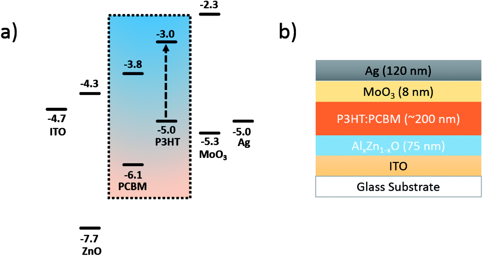 | ||
| Fig. 1 The energy level alignment (a) and device structure (b) in an inverted OPV using P3HT:PC61BM (1:1). | ||
Current density–voltage (J–V) measurements of devices were conducted on a computer-controlled Keithley 2400 Source Meter. A xenon lamp (150 W, Newport Co.) equipped with an AM 1.5G filter was used as the light source. The optical power was 100 mW cm−2, calibrated using a broadband power meter (Newport Co.). The external quantum efficiency (EQE) was measured using monochromatic light (Cornerstone 130 Monochromator, Newport Co.). The incident power was measured using a power/energy meter (Newport Co.). Scanning electron microscopic (SEM) and atomic force microscope (AFM) images were recorded using Zeiss Sigma FE-SEM and Asylum Research MFP 3D respectively. Film thickness was measured with a Bruker Dektak XT profilometer. Absorption spectra were measured using a Varian Cary 7000 spectrometer.
Results and discussion
Morphology study
ZnO and AZO nanoparticles with various Al fractions were synthesized using sol–gel method for only one layer on ITO-coated glass. The morphology of the nanoparticles was investigated on these samples. AFM analysis indicates that the thickness of a single layered ZnO and AZO NPs are in the range of 25 ± 3 nm. Thicknesses and resistivity of the ZnO and AZO NPs are shown in Fig. S1 in ESI.† As is shown in the SEM images in Fig. 2(a), the ZnO NPs demonstrated an average diameter of about 10 nm. The particles are uniformly deposited all around the surface. However, due to the agglomeration effect during high temperature treatment, pores and cracks were created all over the film. Therefore, in order to obtain functional OPV devices, multiple depositions are required to avoid direct contact between the polymer active layer and the bottom electrode. In this work, it was found that the Al dopant has strong influence on the size of the synthesized NPs. With the incorporation of only 1% Al, the average size of the NPs reduced significantly to less than 5 nm (Fig. 2b). One possible explanation is that during the synthesis of ZnO and AZO NPs, heating the as-deposited precursor films results in Zn ions reacting with oxygen to form nanocrystalline ZnO particles. Meanwhile the Al dopants behave as impurities that segregate the grain boundaries and prevent the agglomeration, coalescence and growth of larger grains.13,14 The size of the NPs did not show significant reduction when more Al dopants were added (Fig. S2 in ESI†).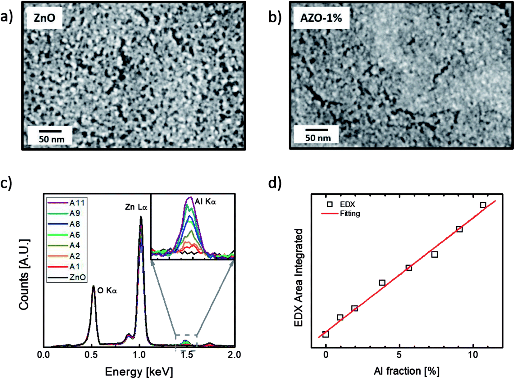 | ||
| Fig. 2 SEM images of 25 nm thick of (a) ZnO and (b) 1%-AZO nanoparticles coated on glass substrate. The ZnO and 1% AZO sample was annealed at 250 °C. (c) EDX spectra of 25 nm thick of AZO films with various Al fraction. The spectra were normalized to the oxygen peak. The Al peak is zoomed in and shown in the insect. (d) Integrated area of the Al peak vs. Al molar ratio in the precursor inks. | ||
The Al composition was studied with EDX. The amount of Al dopants detected in the samples shows a linear relation with the doping concentration, as shown in Fig. 2(c) and (d). The intensity of the Al Kα peak detected in the films increases linearly with the molar ratio of Al ions added to the precursor ink, which indicates the proportional incorporation of Al in the film.
Photovoltaic property
Fig. 3(a) shows the comparison of the current density–voltage (J–V) characteristics of the OPV devices with ETL at different Al fraction. The extracted PV parameters are summarized in Table 1. The J–V curves were performed continuously while the OPV devices were exposed to AM 1.5G illumination, until the devices reached the maximum output. All the parameters listed in Table 1 are extracted from the saturated PV performance. The VOC for the cell with all intermediate layer is approximately 0.57 V; while the short-circuit current demonstrates a slight increase and then decrease with increasing Al doping level. Similar trends are noted for the fill factor and the PCE, which are proportional to the short-circuit current. But overall, the J–V characteristics of all devices have similar PV output, with PCEs between 3.5–4.0%. | ||
| Fig. 3 Photovoltaic performance of the inverted devices using ZnO and AZO as electron transport layers: (a) current density–voltage (J–V) characterizations at the day of fabrication; (b) external-quantum efficiency (EQE) at the day of fabrication; (c) J–V of sample A4 tested at the day of fabrication and 150 days layer; (d) PCE of the sample ZnO within 50 days of fabrication normalized to the highest PCE value. | ||
| Sample | Al fraction in ETL [%] | JSC [mA cm−2] | VOC [V] | FF [%] | PCE [%] |
|---|---|---|---|---|---|
| ZnO | 0 | 12.0 | 0.57 | 51.3 | 3.5 |
| A1 | 1.0 | 12.0 | 0.57 | 53.5 | 3.7 |
| A2 | 2.0 | 12.1 | 0.56 | 53.3 | 3.6 |
| A4 | 4.0 | 12.3 | 0.57 | 56.0 | 3.9 |
| A6 | 5.5 | 12.0 | 0.57 | 53.5 | 3.6 |
| A7 | 7.5 | 12.0 | 0.57 | 52.5 | 3.6 |
| A9 | 9.0 | 11.9 | 0.57 | 51.6 | 3.5 |
| A11 | 11 | 11.7 | 0.56 | 51.9 | 3.4 |
Annealing temperature of the ETL layers is a key factor for fabrication of solar cells with high performance. It has been observed that devices with ZnO ETL show highest PCE when the ZnO was annealed at 250 °C. To reach the same performance, the annealing temperature has to increase for devices with Al-doped NPs ETL. With 1–2% of Al doping, the best conductivity and carrier transfer properties were achieved by rising annealing temperature to 290 °C. For Al fraction higher than 2%, annealing temperature at 320 °C is required to achieve optimum electrical properties. The result is consistent with our previous observation regarding the reduction in size of nanocrystals due to Al doping. The formation of ZnO nanoparticles requires higher energy to incorporate Al impurities into the unit cells and to form uniform film with high conductivity and mobility.15,16
External quantum efficiency (EQE) is defined as the ratio of the number of incident photons and the number of output electrons. It demonstrates the ability of light absorption and charge collection of the solar cells at the same time. Fig. 3(b) shows the EQE curves of the OPV devices from 400 to 800 nm. It is evident that a relative enhancement of EQE at 600 nm occurred for all the Al-doped samples. Similar phenomenon has been reported before.17 As the particle sizes are reduced with Al doping, the surface morphology of AZO layers is likely to be improved in comparison to the ZnO film. Al dopants also introduce electrical polarization into the ZnO lattice, which is likely to influence the wettability. When the P3HT:PCBM ink was spin cast on the ETL, an improvement of ordering could occur during the crystallization of P3HT, and subsequently enhance the quantum efficiency.18
In addition to the tests on the as-fabricated devices, long-term stability tests have also been carried out. All the OPV devices were exposed to air at room temperature for over 5 months. J–V measurements were performed periodically during this time. Fig. 3(c) illustrates the J–V properties measured at the day of fabrication and 150 days later of sample A4 which has 4% Al doped ZnO as ETL. After exposure to ambient environment for 5 months, the Voc and Jsc of the device were nearly unchanged, while the maximum output power decreased by ∼32% (PCE from 3.4% to 2.4%) due to the reduction of FF. Fig. 3(d) illustrates the normalized PCE of a device with ZnO ETL within the first 50 days of air exposure as an example. In contrast to conventional OPV devices, the PCE of our devices first increased for 3–6 days, followed by gradual decline and eventually plateaued at ∼60% of the maximum value. The PCE of devices with Al incorporation show similar enhancing-declining trend as well. The mechanism behind the increasing of PCE in the beginning stage is still under debate, as air and humidity exposure usually causes damages to conventional OPV devices. However, similar phenomenon has been reported for P3HT solar cells with TiOx ETL.19 One possible explanation is that the P3HT molecules are doped with oxygen when exposing to air, and the hole concentration is increased.20 The interfacial electrostatic force between the electron donor and acceptor layers is increased, resulting in a higher efficiency of exciton dissociation and therefore a rising PCE.
Light-soaking effect
To characterize the light-soaking effect, OPV devices were placed under continuous AM 1.5G illumination of 100 mW cm−2. J–V curves of the cells were measured periodically with a certain time interval. The J–V plot of sample A1 is shown in Fig. 4(a). The J–V curve in the beginning stage of the illumination appears as a straight line without rectifying behavior, similar to that of a resistor. Solar devices with such J–V characteristics usually associated with a high series resistance (Rs) and low charge collection rates. With an increasing illumination time, the fill factor and the short-circuit current both increases and the devices start to show J–V characteristics of a diode. During the soaking process, the generated electrons were unable to be transferred to the respective electrode but recombined within the active layer, causing loss to the output power. After enough soaking time under light irradiation, the device parameters reached saturated values. Solar devices with Al doped ZnO ETL were also tested. The FF and PCE values over illumination time of all samples are presented in Fig. 4(b) and (c). Each curve is normalized to the highest FF or PCE value of the respective sample. As seen, the soaking time and the magnitude are directly related to the Al doping fraction. When the Al incorporation reaches more than 4%, the light-soaking effect is eliminated. No shifting of FF or PCE are noticed during the continuous irradiation. Some samples also show decreasing FF and PCE after illumination for a few minutes. This is a typical behavior for OPV devices, which is caused by increased charge scattering and recombination when the surface temperature rises due to irradiation.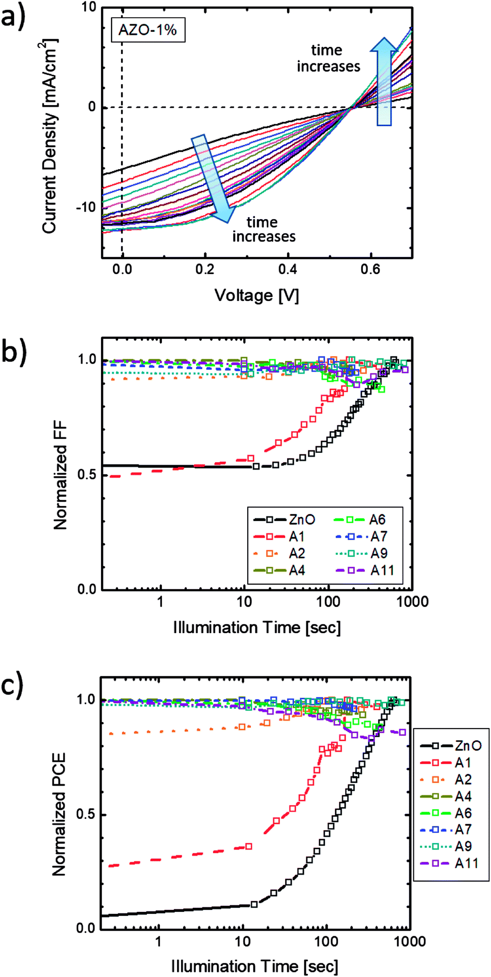 | ||
| Fig. 4 Light-soaking effect in the inverted OPV devices with ZnO/AZO electron transport layers: (a) periodically J–V characterizations of sample A1 measured under continuous light illumination; normalized (b) fill factor and (c) PCE of each sample with illumination time. | ||
In order to understand the light-soaking mechanism, the UV-Visible absorption measurements were performed on glass samples coated with similar ZnO and AZO films to investigate the shifting of the bandgap with Al doping. Each sample was coated with 75 ± 5 nm thick ZnO/AZO particles. The samples were cured in air at 250 °C for ZnO, 290 °C for AZO with 1% Al, and 320 °C for samples with Al concentration > 1%. The absorption spectra (Fig. S3 in ESI†) reveals above 90% transmittance over 400 nm to 800 nm on all the ZnO and AZO thin layers. The optical bandgap is extrapolated from a linear fit to the plot of the squared absorption coefficients vs. photon energy. As shown in Fig. 5(a), the optical bandgap increases with higher Al molar ratio of the NPs. The bandgap shifting is consistent with the well-known Moss–Burstein effect21,22 in which the absorption edge of a semiconductor is pushed to higher energies when charge carriers populate states close to the conduction band. The carrier concentration is increased with more Al incorporation, pushing the Fermi level closer to or even above the original conduction band of ZnO films. Assuming the conduction and valence bands of AZO are parabolic, the bandgap shifting ΔEg and the carrier densities ne follow the relationship:
 | (1) |
 is the effective mass of electrons, and h is the Planck constant. The estimated carrier density in sample A4 is about 1 × 1019 cm−3 if
  is assumed to be 0.17 times of the free electron mass. This value is close to other report electron concentration (in the 1020 cm−3 range) in AZO thin films.14,15,23
 | ||
| Fig. 5 (a) Optical bandgap of ZnO nanoparticles doped with various level of Al; the inset schematic shows the shifting of Fermi level when Al is added into ZnO particles; (b) the simulated band diagram of the inverted OPV devices using ZnO (black lines) and AZO (red lines) with 4% Al electron transport layers. | ||
A numerical simulation based on a modified hetero-PN-junction model was established to calculate the band bending of the inverted OPV devices at 0 V bias. The HOMO and LUMO levels of each layers were obtained from ref. 6, 24 and 25. The carrier concentration of the polymer layers are extracted from the saturated short-circuit current of sample ZnO and A4, while the free electron concentration of ZnO and A4 are obtained from ref. 23 and 26. The thickness of each layer is assumed to be the same as shown in Fig. 1(b), while P3HT and PCBM layers each takes half of the BHJ thickness.
Trost et al. believes that by shifting the Fermi level closer to the conduction band, the pre-existing mismatch between the conduction band of PCBM and ZnO would be reversed for PCBM and AZO interfaces.8 In addition, the opposite interface dipoles could lead to the transport of the generated electrons to the AZO side. However, as the conduction band of ZnO and AZO remains at the same energy, shifting of the Fermi level will only bend the conduction band of both layers, as illustrated in Fig. 5(b). The interfacial dipoles will remain in the same direction, as the barrier is the same as it without Al doping.
As shown in Fig. 5(b), the interface between ITO and ZnO/AZO should be considered as a Schottky contact instead of an ohmic contact since there is a 0.4 eV mismatch between the conduction band of ZnO/AZO and the work function of ITO. When the free carrier density is low in the ETL, the entire layer is depleted to create enough bending on the conduction band to match with the adjacent PCBM and ITO layers. The generated electrons are then swept back to the BHJ and recombined with the generated holes, causing a low charge collection rate. When Al dopant is introduced into the ZnO lattice, the free carrier density in the ETL layer is increased and the depletion region on both sides of the AZO layer is reduced. Eventually when the depletion region is narrow enough to allow the generated electrons tunneling through the barriers, the J–V curves of the devices saturate and the light-soaking effect is fully eliminated. UV exposure, which injects photons with higher energy than the bandgap of ZnO, would excite bonded electrons in the ZnO to the conduction band and increasing the carrier density. Henceforth, the OPV devices will show saturation after a certain exposure time. Once the UV light is removed, the carrier density in ZnO decreases and the layer is again depleted and blocking electron transport.
Conclusions
ZnO and other metal oxides are commonly used in the OPV device fabrication as an electron extraction layer. ZnO nanoparticle ETL can be synthesized with low-cost solution process in ambient environment, with potential for large-scale manufacturing. OPV devices with ZnO ETL and inverted structure have high level of air stability and a prolonged lift-time even without encapsulation. The light-soaking effect is widely observed in the OPV devices using metal oxide ETLs, which causes a major concern in application of the inverted OPV devices. In this paper, we fabricated inverted OPV devices with aluminum doped ZnO electron transport layers. The samples demonstrated high solar harvesting properties with power conversion efficiency up to 3.9%. Air-stability tests of up to 150 days were performed on devices with different Al doping levels. The devices maintained higher than 60% of the initial PCE after 50 days of open-air exposure. The mechanism of the light-soaking effect was investigated with experiments and simulations. The effect can be fully eliminated when the Al fraction in the AZO ETL is higher than 4%. The simulated band diagram of the OPV devices indicates that the low carrier density in the ZnO layer is the main reason of the light-soaking effect. The carrier in the thin ZnO layer is fully depleted to match with the conduction band edge of the adjacent PCBM and ITO layers that lead to the generated electrons being blocked from transferring to the ITO electrode. Doping the ZnO layer as well as exposing the devices under UV irradiation will introduce additional free carriers into the ETL and reduce the width of the depletion region at both side of the ETL. Electrons therefore gain the opportunity to tunnel through both barriers and transport to the electrode.Conflicts of interest
The authors declare no conflict of interest.Acknowledgements
This work was supported by the Natural Sciences and Engineering Research Council, Canada Foundation for Innovation, and King Faisal University.References
- M. A. Green, Y. Hishikawa, E. D. Dunlop, D. H. Levi, J. Hohl-Ebinger and A. W. Y. Ho-Baillie, Prog. Photovoltaics, 2018, 26, 3–12 Search PubMed
.
- M. P. de Jong, L. J. van IJzendoorn and M. J. A. de Voigt, Appl. Phys. Lett., 2000, 77, 2255–2257 CrossRef CAS
- K. W. Wong, H. L. Yip, Y. Luo, K. Y. Wong, W. M. Lau, K. H. Low, H. F. Chow, Z. Q. Gao, W. L. Yeung and C. C. Chang, Appl. Phys. Lett., 2002, 80, 2788–2790 CrossRef CAS
- Z. C. He, C. M. Zhong, S. J. Su, M. Xu, H. B. Wu and Y. Cao, Nat. Photonics, 2012, 6, 591–595 CrossRef
- G. Chen, T. Wang, C. Li, L. Yang, T. Xu, W. Zhu, Y. Gao and B. Wei, Org. Electron., 2016, 36, 50–56 CrossRef CAS
- B. Gholamkhass, N. M. Kiasari and P. Servati, Org. Electron., 2012, 13, 945–953 CrossRef CAS
- H. Oh, J. Krantz, I. Litzov, T. Stubhan, L. Pinna and C. J. Brabec, Sol. Energy Mater. Sol. Cells, 2011, 95, 2194–2199 CrossRef CAS
- S. Trost, K. Zilberberg, A. Behrendt, A. Polywka, P. Gorrn, P. Reckers, J. Maibach, T. Mayer and T. Riedl, Adv. Energy Mater., 2013, 3, 1437–1444 CrossRef CAS
- C. Y. Nam, J. Phys. Chem. C, 2014, 118, 27219–27225 CrossRef CAS
- A. Manor, E. A. Katz, T. Tromholt and F. C. Krebs, Sol. Energy Mater. Sol. Cells, 2012, 98, 491–493 CrossRef CAS
- H. Schmidt, K. Zilberberg, S. Schmale, H. Flugge, T. Riedl and W. Kowalsky, Appl. Phys. Lett., 2010, 96, 243305 CrossRef
- C. H. Chou, W. L. Kwan, Z. R. Hong, L. M. Chen and Y. Yang, Adv. Mater., 2011, 23, 1282–1286 CrossRef CAS PubMed
- M. J. Mayo and D. C. Hague, Nanostruct. Mater., 1993, 3, 43–52 CrossRef CAS
- N. Hasuike, K. Nishio, K. Kisoda and H. Harima, Jpn. J. Appl. Phys., 2013, 52, 01AC09 CrossRef
- J. Hong, H. Paik, H. Hwang, S. Lee, A. J. Demello and K. No, Phys. Status Solidi A, 2009, 206, 697–703 CrossRef CAS
- N. P. Dasgupta, S. Neubert, W. Lee, O. Trejo, J. R. Lee and F. B. Prinz, Chem. Mater., 2010, 22, 4769–4775 CrossRef CAS
- S. H. Tsai, S. T. Ho, H. J. Jhuo, C. R. Ho, S. A. Chen and J. H. He, Appl. Phys. Lett., 2013, 102, 253111 CrossRef
- M. T. Lloyd, R. P. Prasankumar, M. B. Sinclair, A. C. Mayer, D. C. Olson and J. W. P. Hsu, J. Mater. Chem., 2009, 19, 4609–4614 RSC
- C. S. Kim, S. S. Lee, E. D. Gomez, J. B. Kim and Y. L. Loo, Appl. Phys. Lett., 2009, 94, 113302 CrossRef
- M. S. A. Abdou, F. P. Orfino, Y. Son and S. Holdcroft, J. Am.
Chem. Soc., 1997, 119, 4518–4524 CrossRef CAS
- J. J. Jia, A. Takasaki, N. Oka and Y. Shigesato, J. Appl. Phys., 2012, 112, 013718 CrossRef
- R. M. Sternheimer, Phys. Rev., 1954, 93, 642–643 CrossRef CAS
- J. S. Kim, J. H. Jeong, J. K. Park, Y. J. Baik, I. H. Kim, T. Y. Seong and W. M. Kim, J. Appl. Phys., 2012, 111, 123507 CrossRef
- R. J. Davis, M. T. Lloyd, S. R. Ferreira, M. J. Bruzek, S. E. Watkins, L. Lindell, P. Sehati, M. Fahlman, J. E. Anthony and J. W. P. Hsu, J. Mater. Chem., 2011, 21, 1721–1729 RSC
- J. Q. Zhong, H. Y. Mao, R. Wang, J. D. Lin, Y. B. Zhao, J. L. Zhang, D. G. Ma and W. Chen, Org. Electron., 2012, 13, 2793–2800 CrossRef CAS
- A. Janotti and C. G. Van de Walle, Rep. Prog. Phys., 2009, 72, 126501 CrossRef
Footnote |
| † Electronic supplementary information (ESI) available. See DOI: 10.1039/c8ra07071g |
| This journal is © The Royal Society of Chemistry 2018 |