
 Open Access Article
 This Open Access Article is licensed under a Creative Commons Attribution-Non Commercial 3.0 Unported Licence
Growth temperature dependence of nitrogen doped graphene structure on Pt (111) and analysis of its reactivity with oxygen
Seiji
Obata
 * and
Koichiro
Saiki
* and
Koichiro
Saiki
Department of Complexity Science and Engineering, Graduate School of Frontier Sciences, The University of Tokyo, Kashiwa, Chiba 277-8561, Japan. E-mail: obata@edu.k.u-tokyo.ac.jp
First published on 5th October 2018
Abstract
Nitrogen doping is an effective method for modulating the electronic states and properties of graphene. In particular, chemical vapor deposition using nitrogen-containing organic molecules such as pyridine has been expected to be a facile way to control the doping site and amount of nitrogen. However, the atomic structure of nitrogen-doped graphene (NG) synthesized from such molecules has not been investigated. Furthermore, the nitrogen doping sites of NG synthesized at a high temperature of more than 1000 K have also not been measured. In this study, we carried out Scanning Tunneling Microscopy (STM) measurements on the structure of NG synthesized from pyridine, and elucidated the doping sites. Furthermore, we investigated how the doping of nitrogen atoms affects the reactivity with oxygen molecules to reveal the active site of a carbon alloy catalyst. We found that NG synthesized at 1150 K has nitrogen atoms doped into the pyridinic site, and these pyridinic sites enhance the reactivity to oxygen when comparing the defects with/without nitrogen. These findings will help with the synthesis of NG when controlling the doping sites and the development of a catalyst with high efficiency.
Introduction
Graphene, a monolayer sheet of graphite,1 has received significant attention because of its attractive properties such as high mobility,2 and chemical and mechanical stabilities.3 To add various functional properties to graphene, doping heterogeneous atoms into the graphene network is one of the most effective methods.4 Among the various elements, nitrogen atoms are considered a suitable dopant for graphene owing to their size and electronic state. Some computational calculations have predicted that the doping of nitrogen atoms into graphene will drastically change the properties.5,6 For example, nitrogen doping opens the band gap of graphene.5 Graphene has no band gap, which is a significant obstacle to applying graphene to electric devices. Nitrogen doping is one solution to this problem. Furthermore, nitrogen-doped graphene (NG) can be used as a catalyst for the oxygen reduction reaction (ORR) in the cathode of fuel cells.7,8Therefore, many researchers have been trying to develop NG using various methods such as ion bombardment9,10 and chemical vapor deposition (CVD).11,12 NG has three typical doping sites of graphitic, pyridinic, and pyrrolic sites. It should be mentioned that the doping sites of nitrogen strongly affect the properties of nitrogen-doped carbon materials. For example, we previously reported that the work function of a graphene lattice is decreased by the doping of nitrogen atoms into the graphitic site, but is increased through doping into the pyrrolic and pyridinic sites.13 Therefore, the synthesis of NG through control of the doping sites is quite important. We revealed that the CVD method on Pt (111) using various nitrogen containing organic molecule enables us to synthesize NG with the desired doping sites by choosing the appropriate raw materials.14 However, the atomic structure of NG on Pt (111) synthesized from such organic molecules remains unclear. Furthermore, it is difficult to detect a small amount of nitrogen of less than 1% by XPS, although most of the previous studies have used XPS to reveal the doping sites and the amount of nitrogen. Hence, a direct observation at an atomic resolution is indispensable for an analysis of the growth mechanism of NG and an elucidation of the doping sites in NG of low nitrogen content.15,16 These knowledge regarding the growth of NG will make it possible to synthesize NG with a desired structure and doping sites.
In this article, we report the atomic structures of NG grown at various temperatures based on STM images. We chose pyridine as the raw material as based on our previous report.11 Furthermore, we elucidated how nitrogen doping affects the oxygen adsorption on graphene; the reaction with oxygen is considered the first step of ORR in the fuel cells. Therefore, investigating the mechanism of the reaction between NG and oxygen helps in developing a suitable NG with high efficiency for an ORR reaction.
Methods
All experiments were conducted in a chamber equipped with STM and XPS apparatuses (JEOL Ltd. JSPM 4500). The specimens were kept in an ultra-high vacuum during all of the measurements. The NG was prepared through the following method. First, a Pt (111) substrate was cleaned through repeated cycles of Ar sputtering and annealing. After checking the surface cleanness, pyridine or benzene was supplied to the clean Pt (111), which was kept at elevated temperatures. The amount of pyridine or benzene exposure was 200 L at 1.3 × 10⁻⁴ Pa for 200 s. After this procedure, STM and XPS measurements were conducted at room temperature (RT). All STM images were analyzed using WSxM software.17 Raman spectroscopy was conducted at RT with NRS-3000, JASCO Corporation. The grown films were transferred onto SiO2 (300 nm)/Si substrate using the bubbling method18 to measure Raman spectroscopy.Results and discussion
Synthesis of NG and STM observation
Fig. 1 shows STM images and XPS spectra of the N 1s region of pyridine-derived films grown at 850 and 1000 K. A large number of dome-shaped structures of a few nm in size appeared on Pt (111) after exposure at 850 K. A magnified image of these domes is shown in Fig. 1(b), where no long-range (more than 10 nm) ordered structures appeared. The film grown at 850 K was a disordered material consisting of small domed-structures instead of graphene. The XPS spectra of these films indicated that pyridinic nitrogen is dominant (Fig. 1(c)), which is in good agreement with our previous study.14 The disordered structures shown in Fig. 1(a) have many defects and edges, which suggests that some of the grains were terminated with nitrogen atoms. In contrast, the film grown at 1000 K was composed of flat regions and a disordered structure, as shown in Fig. 1(d). The magnified image of this flat region (Fig. 1(e)) shows a clear honeycomb structure without any defects or disorder. Therefore, graphene grew on Pt (111) from pyridine at 1000 K, despite the domain size being about tens of nm2. These results indicate that both the decomposition of the pyridine and the lateral growth of the graphene proceeded further at higher temperature. Although the graphene partially grew on Pt (111), a disordered area remained around the flat area of the graphene. A temperature of 1000 K was insufficiently high to decompose the pyridine completely, and a synthesis of the graphene, which has a large domain size, was not achieved. In the XPS measurement, nitrogen could not be detected at all (Fig. 1(f)). This is consistent with the reduction of the disordered structure, which leads to a reduction of edges or defects where nitrogen atoms are preferably doped.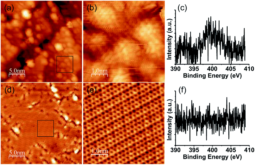 | ||
| Fig. 1 STM images and XPS spectra of the N 1s region of NG grown (a), (b), (c) at 850 K, (d), (e), (f) at 1000 K. (b) and (e) are magnified images of the black rectangle in (a) and (d), respectively. | ||
To obtain a more crystalline specimen, we increased the growth temperature to 1150 K. Fig. 2(a) shows a wide range of STM images of the specimen. A step and terrace structure with several moiré patterns separated by the domain boundaries was observed. The area with the same moiré pattern ranged from tens to hundreds of nm2. Fig. 2(b) shows a magnified image of the area around the domain boundary shown in the lower part of Fig. 2(a). The appearance of these clear moiré structures proves the growth of monolayer graphene on Pt (111). The moiré pattern on the right side differs from that of the region on the left, which indicates polycrystalline graphene growth with various orientation angles between Pt (111). The magnified image of the rectangle area in Fig. 2(b) shows a clear honeycomb lattice without any defects (Fig. 2(c)). These results reveal that monolayer graphene with high crystallinity grew on the entire Pt (111) surface using pyridine as the raw material at 1150 K. Fig. 2(d) shows an STM image of graphene at around a Pt (111) step at an atomic resolution. The moiré structure is continuous over the step of Pt (111), and no disordered structures or defects were observed around the step. Graphene grew in carpet mode on Pt (111), which enables the growth of a single large domain of graphene over the Pt (111) steps. In the XPS measurement, nitrogen could not be detected.
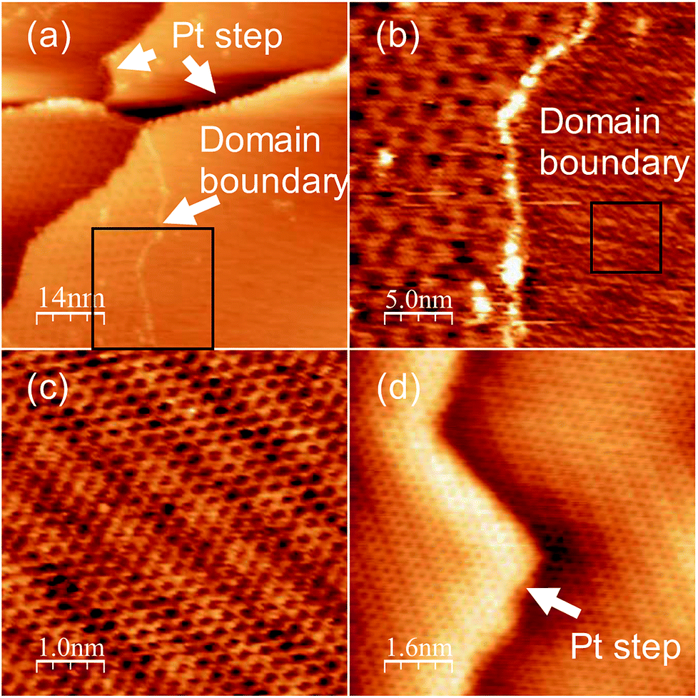 | ||
| Fig. 2 STM image of NG grown at 1150 K. (a) Large-scale image with Pt (111) step and domain boundary, and (b) magnified image of the rectangle area in (a). (c) Magnified image of the rectangle area in (b). (d) Atomic-resolution image at around a Pt (111) step. | ||
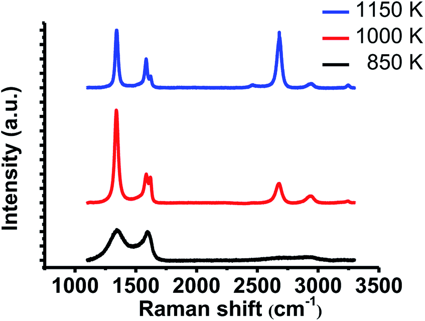
We also conducted Raman spectroscopy to evaluate the crystallinity of the grown films. Raman spectra were measured on SiO2/Si substrates after the transfer process. Fig. 3 indicates the typical spectra of the films grown at each temperature. NG grown at 1150 K shows larger 2D band (∼2678 cm−1) than G band (∼1583 cm−1), which proves monolayer graphene growth. In addition to these two peaks, large D band (∼1341 cm−1) and D′ band (1621 cm−1) also appeared. Large D′ band is characteristic of NG.19 Therefore, this result indicates that NG was grown at 1150 K. The film grown at 1000 K shows larger D band and D′ band with smaller 2D band. It means that this film has more incorporated nitrogen atoms and lower crystallinity compared with the specimen grown at 1150 K. In contrast, the film grown at 850 K shows large and broad G band and D band with slight 2D band, which indicates the disordered film growth. These results are consistent with the STM results.
 | ||
| Fig. 3 Raman spectra of the grown films after the transfer onto SiO2/Si substrate. All spectra were normalized to the intensity of G band. | ||
These results of graphene growth at various temperatures revealed that the growth of larger graphene with higher crystallinity occurs as the growth temperature increases. However, the amount of nitrogen decreased with the increase in the growth temperature. Pyridine does not completely decompose at 850 K, which leads to an incorporation of nitrogen atoms into the grown structure. However, owing to the insufficient decomposition, the growth of graphene with high crystallinity was impossible. As a result, a disordered structure with nitrogen edges appeared. In contrast, graphene with high crystallinity grew at 1150 K, and the nitrogen content was less than 1% at most. This means that it is difficult to grow graphene of high crystallinity with a large amount of nitrogen, because the growth of high crystallinity graphene requires high temperature, and nitrogen easily evaporates at such a high temperature.
Although the graphene grown at 1150 K has high crystallinity, we found some different structures from a normal graphene lattice. Fig. 4 shows some typical examples, namely, at the domain boundaries and in bright regions in a honeycomb lattice. A magnified image of the domain boundary is shown in Fig. 4(a). The structure was disordered, and there are some bright areas at the domain boundary. Other examples, namely, bright patterns in the basal plane, are shown in Fig. 4(b) and (c). We found several types of bright patterns in the basal plane of graphene, and the brightness changed over a few carbon atoms. These brightness modulations might be caused by an incorporation of nitrogen atoms. It should be noted that a number of such sites were too small to be detected using XPS spectra. To elucidate whether nitrogen in a honeycomb lattice practically causes such a brightness modulation, a comparison with the theoretical calculation is required.
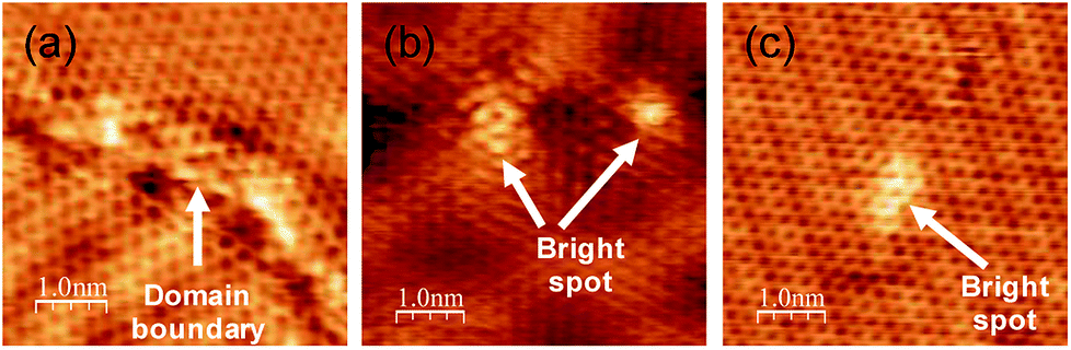 | ||
| Fig. 4 STM image of NG grown at 1150 K at around (a) domain boundary and (b), (c) bright spots. | ||
Structural analysis of defects with and without nitrogen
We then focused on the bright patterns around the defects, which can be compared with the theoretical calculations. Fig. 5(a) shows an STM image of graphene made from pyridine at 1150 K. Two different types of defects were observed in the honeycomb lattice and moiré pattern. The defects marked with circles are brighter than the defects marked with rectangles. These two defects have different patterns of brightness around them, which reflects the difference in the atomic structure. A magnified image of these two types of defects is shown in Fig. 5(b). The brighter defect shows a bright pattern of a triangle shape, one side of which is brighter than the others. The darker defect has a slightly brighter side than the other sides. To elucidate these atomic structures, we compared these bright patterns with the theoretical calculations. Some theoretical calculations of the electronic states around the defects of graphene with/without nitrogen were conducted. Hou et al. reported the electronic states around various types of defects.20 Ana et al. also reported the simulated electronic state of pyridinic sites on Pt (111).21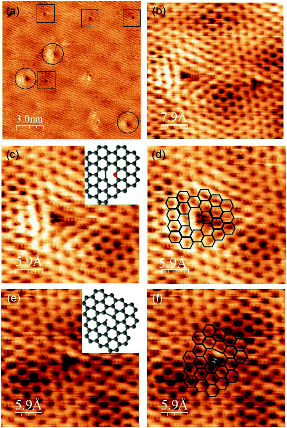 | ||
| Fig. 5 (a) and (b) STM images of two types of defects in NG grown at 1150 K. Vs: 10 mV (c) magnified image of left-hand defect in (b), inset: model of the structure. (d) Magnified images with chemical structure. (e) Magnified images of right-hand defect in (b), inset: model of the structure. (f) Magnified image with chemical structure. | ||
Comparing our STM data with their calculations, the bright pattern of the left image in Fig. 5(b) is considered to consist of pyridinic nitrogen and five-membered ring carbon (Fig. 5(c) and (d)). This analysis of the atomic structure of NG proved that nitrogen-doped graphene with high crystallinity was synthesized from pyridine on Pt (111) at 1150 K. The number of these types of defects was quite low. Therefore, it is reasonable that we cannot detect them through XPS. In contrast, according to Hou's calculations, the brightness pattern on the right nearly corresponds to the structure consisting of hydrogen-terminated carbon atoms out of the graphene plane and close to the Pt (111) surface, and a five-membered ring (Fig. 5(e) and (f)). Ugeda et al. reported the experiment and theoretical STM images of a single-carbon vacancy without nitrogen and hydrogen on Pt (111).22 The brightness pattern around this type of defect also resembles the one on the right. Although, it is difficult to judge whether the defect on the right contained hydrogen, we concluded that the defect on the left contains nitrogen atoms and the one on the right does not.
Oxygen adsorption on NG
Because we can compare these two defects under the exact same conditions, this specimen, with two defect sites with and without nitrogen, is an appropriate sample for revealing the effects of incorporated nitrogen on the oxygen adsorption. We exposed this specimen to 10 L (1.3 × 10−5 Pa × 100 s) of oxygen at RT and measured it using STM imagery in a vacuum. Fig. 6(a) and (b) show an STM image of the defects before and after exposure to 10 L of oxygen. The brightness pattern of the defect on the left drastically changed after the exposure of 10 L oxygen. In contrast, the defect on the right remained the same. After that, we exposed the specimen to additional 1000 L of oxygen. After the exposure of 1010 L oxygen, a bright area with the height of about 0.15 nm (Fig. 6(c) and (d)) appeared around the defect on the left, while the defect on the right remained unchanged. Although the manner in which the atomic structure of the defect with nitrogen changed by such exposure remains unclear owing to a lack of calculated results, we can conclude that the defect with nitrogen atoms reacted with the oxygen gas even at RT, and a change in structure therefore occurred. In contrast, the defect without nitrogen atoms did not change after oxygen exposure. Our results show that the nitrogen atoms incorporated into the graphene lattice in this manner enhance the reactivity to oxygen. These results are consistent with a spectroscopic and electrochemical study conducted by Guo et al., who elucidated that the active sites for an oxygen reduction reaction are pyridinic sites.23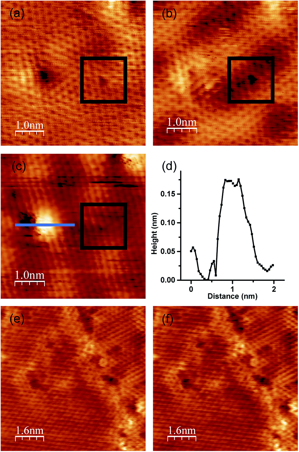 | ||
| Fig. 6 STM images of graphene from pyridine and benzene grown at 1150 K. (a) As-grown NG, (b) NG after exposure to 10 L of oxygen, (c) NG after exposure to 1010 L of oxygen. Vs: 100 mV. Black rectangles indicate the defect on the right. (d) Height profile along the blue line in (c). (e) As-grown graphene from benzene. (f) Graphene after exposure to 10 L of oxygen. Vs: 20 mV. | ||
To elucidate the role of nitrogen atoms, we synthesized graphene from benzene on Pt (111) at 1150 K. Graphene from benzene also has a disordered structure such as domain boundaries and defects, as shown in Fig. 6(e). However, these disordered structures did not contain any nitrogen atoms. After the growth, we also exposed oxygen to graphene from benzene. We focused on the atomic structure around a domain boundary with some defects to elucidate the oxygen adsorption on both an ordered honeycomb lattice and disordered structures. No structural or brightness changes were observed even around the defects after exposure to 10 L of oxygen (Fig. 6(f)). All STM results regarding oxygen exposure indicate that the defect site with nitrogen doped at the pyridinic site enhances the reactivity of graphene with oxygen.
Conclusions
In summary, we investigated the growth temperature dependence of a nitrogen-doped graphene structure grown on Pt (111) from pyridine. At a low temperature of 850 K, a domed shape structure with nitrogen atoms doped into the pyridinic sites appeared. As the growth temperature increased, the nitrogen content decreased, and the graphene domain became lager. We analyzed the bright spots in NG grown at 1150 K and elucidated that nitrogen was doped at the pyridinic site. As such, we succeeded in synthesizing nitrogen-doped graphene with high crystallinity. Furthermore, we investigated the effects of nitrogen atoms on the oxygen adsorption at atomic resolution through a comparison between two types of defects. Only the defect with nitrogen doped into the pyridinic site changed the electronic state after exposure. We concluded that nitrogen doped at the pyridinic site enhances the reactivity with oxygen. Elucidation of the atomic structure of NG from pyridine and the oxygen adsorption site in this work would be helpful to synthesize the catalyst with high ORR activity for the fuel cells.Conflicts of interest
There are no conflicts of interest to declare.Acknowledgements
This work was supported by JSPS KAKENHI Grant Numbers JP25790001 and JP18K04881.References
- K. S. Novoselov, A. K. Geim, S. V. Morozov, D. Jiang, Y. Zhang, S. V. Dubonos, I. V. Grigorieva and A. A. Firsov, Science, 2004, 306, 666–669 CrossRef CAS.
- K. I. Bolotin, K. J. Sikes, Z. Jiang, M. Klima, G. Fudenberg, J. Hone, P. Kim and H. L. Stormer, Solid State Commun., 2008, 146, 351–355 CrossRef CAS.
- C. Lee, X. Wei, J. W. Kysar and J. Hone, Science, 2008, 321, 385–388 CrossRef CAS PubMed.
- X. Wang, G. Sun, P. Routh, D.-H. Kim, W. Huang and P. Chen, Chem. Soc. Rev., 2014, 43, 7067–7098 RSC.
- P. Rani and V. K. Jindal, RSC Adv., 2013, 3, 802–812 RSC.
- Z. Hou, X. Wang, T. Ikeda, K. Terakura, M. Oshima and M. A. Kakimoto, Phys. Rev. B: Condens. Matter Mater. Phys., 2013, 87, 1–16 CrossRef.
- T. Ikeda, M. Boero, S. F. Huang, K. Terakura, M. Oshima and J. Ozaki, J. Phys. Chem. C, 2008, 112, 14706–14709 CrossRef CAS.
- L. Qu, Y. Liu, J. B. Baek and L. Dai, ACS Nano, 2010, 4, 1321–1326 CrossRef CAS.
- T. Kondo, S. Casolo, T. Suzuki, T. Shikano, M. Sakurai, Y. Harada, M. Saito, M. Oshima, M. I. Trioni, G. F. Tantardini and J. Nakamura, Phys. Rev. B: Condens. Matter Mater. Phys., 2012, 86, 1–6 CrossRef.
- W. Zhao, O. Höfert, K. Gotterbarm, J. Zhu, C. Papp and H.-P. Steinrueck, J. Phys. Chem. C, 2012, 116, 5062–5066 CrossRef CAS.
- G. Imamura and K. Saiki, J. Phys. Chem. C, 2011, 115, 10000–10005 CrossRef CAS.
- Y. F. Lu, S. T. Lo, J. C. Lin, W. Zhang, J. Y. Lu, F. H. Liu, C. M. Tseng, Y. H. Lee, C. Te Liang and L. J. Li, ACS Nano, 2013, 7, 6522–6532 CrossRef CAS.
- K. Akada, T. Terasawa, G. Imamura, S. Obata and K. Saiki, Appl. Phys. Lett., 2014, 104, 131602 CrossRef.
- T. Katoh, G. Imamura, S. Obata and K. Saiki, RSC Adv., 2016, 6, 13392–13398 RSC.
- L. Pauling, G. H. Wannier, L. Balents, S. Sachdev, R. Moessner, A. P. Ramirez, I. Bloch, J. Dalibard, W. Zwerger, B. Dakic, W. Naylor, A. Zeilinger and P. Walther, Science, 2011, 333, 999–1004 CrossRef.
- R. Lv, Q. Li, A. R. Botello-Méndez, T. Hayashi, B. Wang, A. Berkdemir, Q. Hao, A. L. Eléas, R. Cruz-Silva, H. R. Gutiérrez, Y. A. Kim, H. Muramatsu, J. Zhu, M. Endo, H. Terrones, J. C. Charlier, M. Pan and M. Terrones, Sci. Rep., 2012, 2, 1–8 Search PubMed.
- I. Horcas, R. Fernández, J. M. Gómez-Rodríguez, J. Colchero, J. Gómez-Herrero and A. M. Baro, Rev. Sci. Instrum., 2007, 78, 013705 CrossRef CAS.
- L. Gao, W. Ren, H. Xu, L. Jin, Z. Wang, T. Ma, L. P. Ma, Z. Zhang, Q. Fu, L. M. Peng, X. Bao and H. M. Cheng, Nat. Commun., 2012, 3, 697–699 CrossRef.
- L. Gao, W. Ren, H. Xu, L. Jin, Z. Wang, T. Ma, L. P. Ma, Z. Zhang, Q. Fu, L. M. Peng, X. Bao and H. M. Cheng, Nat. Commun., 2012, 3, 697–699 CrossRef.
- Z. Hou, X. Wang, T. Ikeda, K. Terakura, M. Oshima and M. A. Kakimoto, Phys. Rev. B: Condens. Matter Mater. Phys., 2013, 87, 1–16 CrossRef.
- A. Martín-Recio, C. Romero-Muñiz, P. Pou, R. Pérez and J. M. Gómez-Rodríguez, Nanoscale, 2016, 8, 17686–17693 RSC.
- M. M. Ugeda, D. Fernández-Torre, I. Brihuega, P. Pou, A. J. Martínez-Galera, R. Pérez and J. M. Gómez-Rodríguez, Phys. Rev. Lett., 2011, 107, 1–5 CrossRef.
- D. Guo, R. Shibuya, C. Akiba, S. Saji, T. Kondo and J. Nakamura, Science, 2016, 351, 361–365 CrossRef CAS.
| This journal is © The Royal Society of Chemistry 2018 |