
 Open Access Article
 This Open Access Article is licensed under a Creative Commons Attribution-Non Commercial 3.0 Unported Licence
Traceless mitigation of laser damage precursors on a fused silica surface by combining reactive ion beam etching with dynamic chemical etching
Laixi Sun a,
Ting Shaoa,
Jianfeng Xub,
Xiangdong Zhoub,
Xin Yea,
Jin Huanga,
Jian Baib,
Xiaodong Jianga,
Wanguo Zhengc and
Liming Yang*a
a,
Ting Shaoa,
Jianfeng Xub,
Xiangdong Zhoub,
Xin Yea,
Jin Huanga,
Jian Baib,
Xiaodong Jianga,
Wanguo Zhengc and
Liming Yang*a
aResearch Centre of Laser Fusion, China Academy of Engineering Physics, Mianyang 621900, China. E-mail: yanglcaep@163.com
bState Key Laboratory of Modern Optical Instrumentation, Zhejiang University, Hangzhou 310027, China
cIFSA Collaborative Innovation Center, Shanghai Jiao Tong University, Shanghai 200240, China
First published on 18th September 2018
Abstract
HF-based etching has been successful in mitigating damage precursors on the surface of fused silica optics used in high power lasers. However, wet etching generally leaves an etching trace leading to surface roughness, which seriously degrades laser beam quality (e.g., transmission loss and wave-front degradation). A way of addressing this issue is to apply plasma etching as a preprocessing step before HF etching, but so far very few studies have provided a practical scheme for engineering applications. In this work, we proposed a novel two-step scheme by combining reactive ion beam etching with dynamic chemical etching techniques. We demonstrate the combined scheme is capable of tracelessly mitigating the laser damage precursors on a fused silica surface. The 0% probability damage threshold obtained by combined etching is 1.4 times higher than that obtained by HF-based etching. The study opens a new approach towards high damage-resistant optics manufacturing and provides the potential possibility of exploring extreme interactions between high-power lasers and matter.
Introduction
Since laser-induced damage (LID) on fused silica surfaces radically limits the lifetime of optics in high-power fusion-class laser systems such as the National Ignition Facility,1 the Megajoule laser2 or SG-III,3 damage precursors have been investigated extensively aiming at improving the laser-induced damage threshold (LIDT) of fused silica.4–9 Although recent efforts in HF-based chemical etching have succeeded in dramatically improving the damage resistance of fused silica,10–12 they remain limited to the surface quality after etching.13,14 The root cause of the surface quality degradation is chemical treatment leaving etching traces (scratches and pits are opened and extended into geometrical structures), which lead to the increase of surface roughness and figure errors. This has greatly restricted fused silica optical components working at high-fluence laser facilities from attaining excellent laser-beam quality.Plasma etching is ideal for surface modification of fused silica as they present anisotropic means to remove the physical-structure defects (e.g., scratches or pits) without any trace and thus smooth the optical surface.15 Although chemical structure defects such as oxygen-deficiency center (ODC) or others might be generated during plasma etching,16 HF-etching can be used as a next step to remove them. In our previous letter,17 we evidenced the combined process of reactive ion etching (RIE) and dynamic chemical etching (DCE) is an effective method for significantly improving the damage resistance of fused silica optics while keeping the surface quality non-degraded. However, this method is also limited to processing flexibility and applicability since the effective etching region in conventional RIE systems is relatively immutable when the etching process is fixed. The etching uniformity is seriously influenced by the limited plasma density distribution.18,19 Completely being different with RIE in plasma generating principle, reactive ion beam etching (RIBE) show great promise for flexibly modifying fused silica surface since the ion energy, beam density, as well as the chemical reaction extent, can be independently controlled. More importantly, the etching uniformity can be effectively improved by moving or rotating the sample stage to finish the total required etching-area.20–22 Yet to the best of our knowledge, very few reports have focused on the damage resistance enhancement by using RIBE technique, even the combination of RIBE and DCE has not been applied as a means of improving the damage threshold of fused silica optics.
In this work, we mainly focused on the effects of the combined process of RIBE and DCE on damage performance and surface quality of fused silica optics. The RIBE pretreatment was used to tracelessly remove the physical-structure defects on fused silica surface. Then the DCE retreatment was used to remove the RIBE-introduced defects and passivate the optical surface. This combined technique of RIBE and DCE was demonstrated to be a better method for improving the damage performance and surface quality of fused silica optics than single RIBE and single DCE technique. The study provides a potential probability for this combined etching technique applying to manufacture high quality fused silica optics and paves the way towards the comprehension of the damage mechanism of fused silica at high-energy nanosecond laser facilities.
Experimental
During the experiments, a series of fused silica samples were treated by single RIBE, single DCE and the combined etching processes. Unetched sample and the single treated sample were used as references. For the combined etching process, a single-sided RIBE process was used as the first step to remove the fractured defects in the subsurface layer of fused silica. The RIBE-treated side was regarded as the rear surface for damage test. Subsequently, a double-sided DCE process was adopted to remove the RIBE-introduced defects and passivate the optical surface of fused silica. Considering that RIBE treatment has much stronger physical-bombardment ability than RIE treatment, we thus optimized the DCE procedure, which includes three steps: (1) an inorganic acid cleaning process to dissolve the possible contaminants (metallic impurities and/or fluorocarbon deposits) introduced by RIBE, (2) a weak alkali cleaning process to remove trace oil and dirt, and (3) a buffered HF-based etching process to remove and passivate the unstable chemical structure on fused silica surface. A flow chart of the combined process is given in Fig. 1.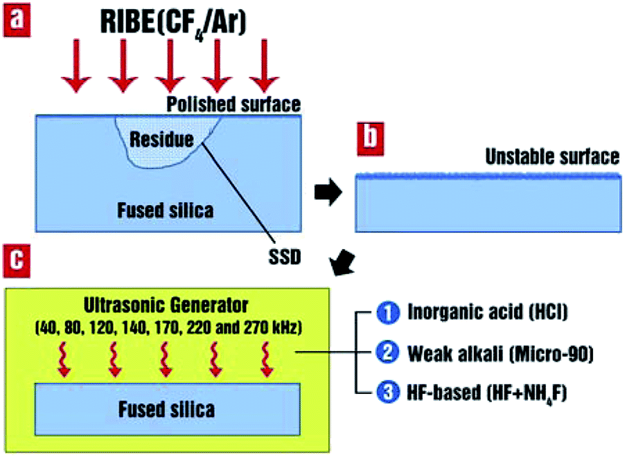 | ||
| Fig. 1 Detailed description of the combined process of RIBE and DCE. | ||
Square samples (50 mm wide and 5 mm thick) made of Corning 7980 were manufactured by the same vendor using traditional polishing process. Samples were all cleaned with high pure water under ultrasonic condition before the RIBE treatment, damage test and other characterizations.
A commercial RIBE system was used for the plasma modification investigation. The Ar-CF4 plasma beam was generated by a broad-beam (150 mm aperture) Kaufman-type DC ion source which was fitted with molybdenum grids. The beam was neutralized by electrons emitted from a hot tungsten filament neutralizer located in front of the grids. During the RIBE process, ultrapure argon and CF4 gas (99.999%) were supplied to the ion source through mass flow controllers. The grid current, acceleration voltage and working pressure were about 80 mA, 550 V and 2 × 10⁻² Pa, respectively. The fused silica sample was fixed onto a water-cooled rotating stage (6 rpm) with the ion beam vertically incident to the sample surface.
The whole DCE process was carried out under ultrasonic conditions using a Teflon-lined, multi-frequency ultrasonic transducer (Blackstone multiSONIK™ 40, 80, 120, 140, 170, 220 and 270 kHz) in which the samples were constantly mounted with their edges held still. During the inorganic acid cleaning process, the samples were all submerged in silica tanks filled with mixed inorganic acid consisting of 36 wt% HCl and deionized water with a volume ratio of 1![[thin space (1/6-em)]](https://www.rsc.org/images/entities/char_2009.gif) :2. The processing time was 120 min. Subsequently, the samples were removed and rinsed with deionized water. The weak alkali cleaning process was conducted in silica tanks filled with a 10 vol% solution of Micro-90 (a commercial cleaning agent). The processing time was 30 min. The HF-based etching process used as the last step of the DCE treatment was implemented in Teflon-lined tanks. HF and NH4F solution was used to etch fused silica. The detailed etching process has been described elsewhere.17 After the DCE treatment, the samples were cleaned again with deionized water and allowed to air dry. The cleaning, etching, and drying processes were totally implemented in a class 100 clean room.
:2. The processing time was 120 min. Subsequently, the samples were removed and rinsed with deionized water. The weak alkali cleaning process was conducted in silica tanks filled with a 10 vol% solution of Micro-90 (a commercial cleaning agent). The processing time was 30 min. The HF-based etching process used as the last step of the DCE treatment was implemented in Teflon-lined tanks. HF and NH4F solution was used to etch fused silica. The detailed etching process has been described elsewhere.17 After the DCE treatment, the samples were cleaned again with deionized water and allowed to air dry. The cleaning, etching, and drying processes were totally implemented in a class 100 clean room.
Results and discussion
Prior to the RIBE pretreatment, the etching rate and uniformity were first investigated to verify the etching ability of the system. This experiment was implemented using a square fused silica sample with 100 mm wide and 5 mm thick. Fig. 2 shows the etching rate as a function of gas flow ratio R (CF4/Ar). Three typical regions were divided by two Rs, 1.5 and 2.5, respectively. The etching rate in low R region (yellow color) was very low because the etching process in this region was mainly dominated by physical bombardment of the energetic ions. In the green region, there was a sharp increase in etching rate, which was attributed to the great increase of chemical etching. Additionally, the physical bombardment also enhanced the chemical reaction. When the gas flow ratio further increased (red color), the etching rate kept stable. It is probably due to the ionization rate of fluorine-containing species reaching saturation as the input power was fixed. Besides, polymer deposition may easily occur on the sample surface in this region, which suppresses the chemical etching. To effectively remove the physical-structure defects (scratches or pits in subsurface layer) in the sample surface, physical bombardment should be enhanced to increase the anisotropic etching of the ion beam. Our previous study also evidenced smooth optical surface of fused silica can be obtained by increasing the physical bombardment ability during the plasma etching process.23 We thus believe the RIBE in low R region is beneficial to the removal of the physical-structure defects.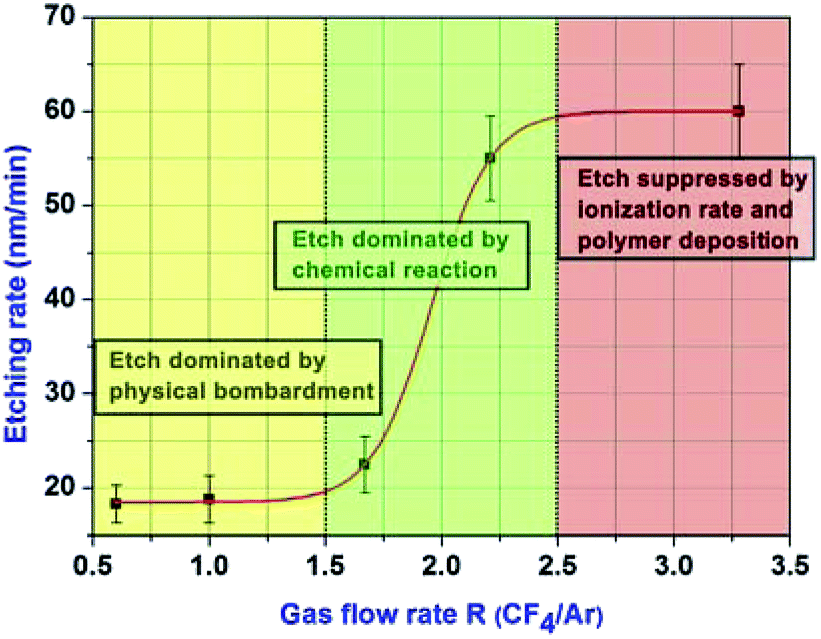 | ||
| Fig. 2 Etching rate as a function of gas flow ratio R (CF4/Ar). Three regions with yellow, green and red color were divided by two Rs. | ||
Plasma etching of fused silica is often accompanied by chemical-structure damage. We thus measured the laser-induced fluorescence (FL) of the samples to analyse the chemical-structure defects introduced by the RIBE treatment. Three samples used for the measurement were treated by RIBE with different R values of 3.28, 2.21 and 0.6, respectively corresponding to different regions mentioned in Fig. 2. The etching time for all the samples was 80 min. An unetched sample was used as a reference. Hydrochloric acid cleaning process was conducted prior to FL measurement to exclude the effect of the RIBE-introduced impurities on the FL results. To make the fluorescence data more reliable, the measurement location and direction for each sample were strictly fixed. Fig. 3 shows the FL emission spectra of the samples etched with different gas flow ratio Rs. For all the samples, the emission spectra were dominated by FL peaks centered on 3.2–3.3 eV, which have been attributed to the oxygen-related defects such as ODC. It's very important to note that the FL intensity of the RIBE-treated samples was increased with the gas flow ratio R. Especially for the R value of 3.28, the defect-induced FL was obvious and the emission spectrum was redshifted. The results indicate that the RIBE with low R value is beneficial to suppress the chemical-structure defects induced by the RIBE treatment.
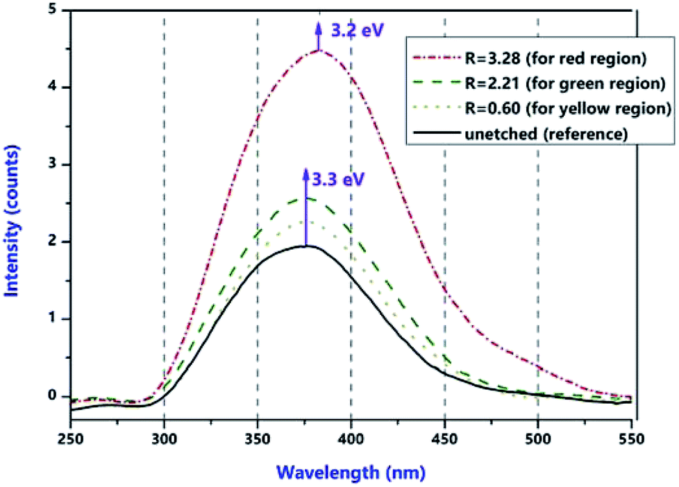 | ||
| Fig. 3 Fluorescence emission spectra excited by a peak centered at 283 nm (5.0 eV) for the samples etched with different gas flow ratio Rs. A unetched sample was used as a reference. The etching time for all the samples was 80 min. | ||
To enhance the anisotropic etching effect while suppress the etching-induced FL defects, we chose the gas flow ratio R of 0.6 for the subsequent etching experiments. The etching uniformity of the RIBE process was shown in Fig. 4. In the case, if the acceptable deviation for etching depth was 5% of the maximum value,24 the uniform etching region was a circle with the radius of about 40 mm. The results suggested that this RIBE system was suitable for uniformly modifying the samples we chose for the experiments. For larger samples, we can use scanning etching process by moving the position of the sample stage or changing a larger ion beam source, which is obviously not our focus in this study.
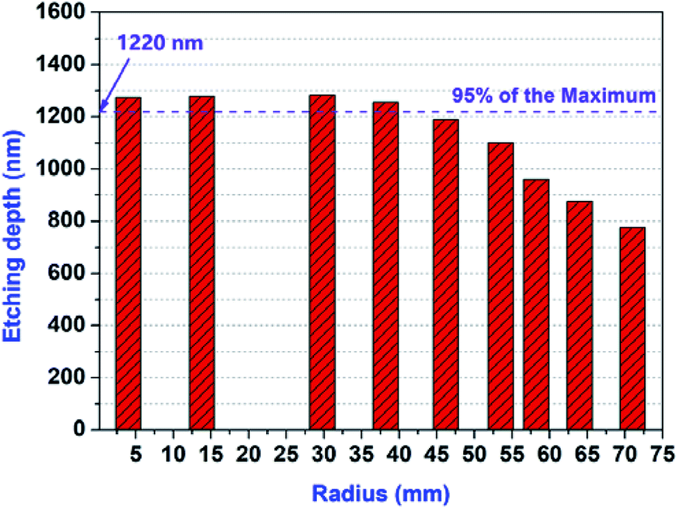 | ||
| Fig. 4 Etching depth along the radial direction of the sample stage. The gas flow ratio R was fixed to be 0.6. The black line at 1220 nm represents the acceptable deviation (5%) to the maximum value. | ||
The samples with various etching processes (no etching, single RIBE, single DCE and the combined etching) were damage tested. A near-Gaussian 355 nm laser beam with a diameter of 1.2 mm at 1/e2 was delivered by a pulsed Nd:YAG laser system. The pulse width of the laser beam was ∼7 ns. The uncertainty of the energy density in the test system is 4.5%. The detailed description for the testing system can be found elsewhere.25 1-on-1 strategy (ISO 21254) was used for testing the laser damage probability of the samples. Twenty testing sites for each energy density were chosen randomly on the rear surface of fused silica samples. The laser damage probability of the samples treated with different etching processes is shown in Fig. 5. Compared with the unetched sample (black squares), the zero probability LIDT of the 1.5 μm RIBE-treated sample (red circles) was slightly decreased. Obvious increase in LIDT was observed when the samples were undergone a single DCE treatment, especially at 20 μm etching depth. After the combined etching (pink stars), the damage resistance of the sample was dramatically improved. Noted that the damage probability of the sample treated by the combined process was only 10% when the laser fluence was fixed to be about 54 J cm−2 (which was near the maximum output fluence of the laser system). The results indicated that some low-fluence damage precursors must exist on the RIBE-treated sample surface and this kind of defect can be easily removed by the subsequent steps of the combined etching process (Table 1).
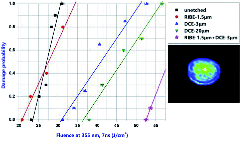 | ||
| Fig. 5 Laser damage probability of the samples treated with various etching processes. The solid lines denote the linear fitting curves of the measured damage probability. The inset in the lower right corner is the laser spot profile with a modulation degree of 2.1. | ||
| Samples | Damage threshold of 0% probability (J cm−2) | Damage threshold of 100% probability (J cm−2) |
|---|---|---|
| Unetched | 23.2 | 30.7 |
| RIBE-1.5 μm treated | 20.8 | 34.4 |
| DCE-3 μm treated | 31.2 | 51.1 |
| DCE-20 μm treated | 36.4 | 56.35 |
| RIBE-1.5 μm and DCE-3 μm treated | 52.5 | — |
We then measured the impurity concentration in surface of the samples with various etching processes by Time-of-flight secondary ion mass spectrometry, as shown in Fig. 6. Noted that large number of Na, K and Al impurities deposit on the unetched sample surface, which were attributed to the residual polishing compounds embedded in the redeposition layer of the optics (see Fig. 6(a)). Although most of the impurities were removed by the RIBE treatment, the concentration of the Al element increased obviously (see Fig. 6(b)). The total amount of Al element in the surface of each sample is shown in Table 2. We believe that the Al contamination on the sample surface arose from the physical bombardment of energetic ions onto the chamber inner-wall and/or the sample stage. Indeed, Al contamination is harmful for RIBE treatment to improve the LIDT of fused silica optics since this kind of defect has been evidenced to be photosensitive to absorb the laser energy and initiate the damage.26 It can be noted from Fig. 6(c) and (d) that the optical surfaces treated by the combined etching and single DCE process both had the lowest Al concentration, suggesting the DCE treatment can effectively remove the RIBE-introduced Al impurity. The results also seem to tell us that the hydrochloric acid cleaning process is indispensable once RIBE is used as a pre-processing step before HF etching because RIBE-introduced metallic impurities may form micro-mask on the sample surface, hindering the chemical reaction of HF acid with fused silica.
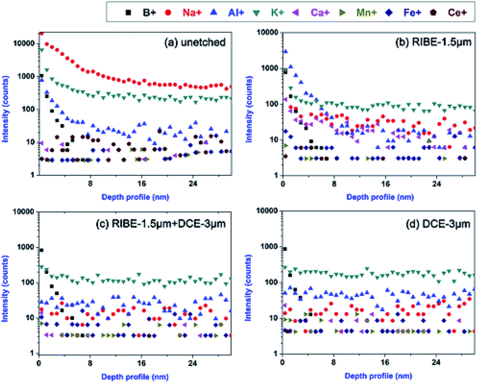 | ||
| Fig. 6 Depth profiles of the impurities in the surfaces for (a) unetched sample; (b) 1.5 μm RIBE-treated sample; (c) 1.5 μm RIBE-pretreated and 3 μm DCE-retreated sample; (d) 3 μm DCE-treated sample. | ||
| Samples | Concentration of Al element |
|---|---|
| Unetched | 4089.8 |
| 1.5 μm RIBE treated | 10330.3 |
| 1.5 μm RIBE and 3 μm DCE treated | 2121.1 |
| 3 μm DCE treated | 3415.6 |
We subsequently observed the morphology of the damage sites on the surface of the samples with different processes, as shown in Fig. 7. The damages were all initiated at their damage thresholds of zero probability. For the unetched sample at the laser fluence of 23.2 J cm−2, the damage sites were smashed and adhered to each other due to the low-fluence damage precursors in the polished sample surface strongly absorbing laser energy and initiating damage. For the 1.5 μm RIBE-treated sample, the density of the damage sites began to decrease at the zero-probability damage threshold of 20.8 J cm−2, suggesting the RIBE-introduced defects could easily induce damage. For the 3 μm DCE-treated sample at 31.2 J cm−2 laser fluence, the damage sites became sporadic and discrete craters with fractured edges because the low-fluence damage precursors in the subsurface layer were significantly removed by the etching, but the damage residues were difficult to be taken away thoroughly at this fluence. For the sample treated by the combined process, the damage sites represented more sporadic craters with smooth edges. At this high laser fluence (52.5 J cm−2), strong laser energy and shock wave could take away nearly all the damage residuals from the fused silica optical surface, forming much cleaner damage cater appearance.
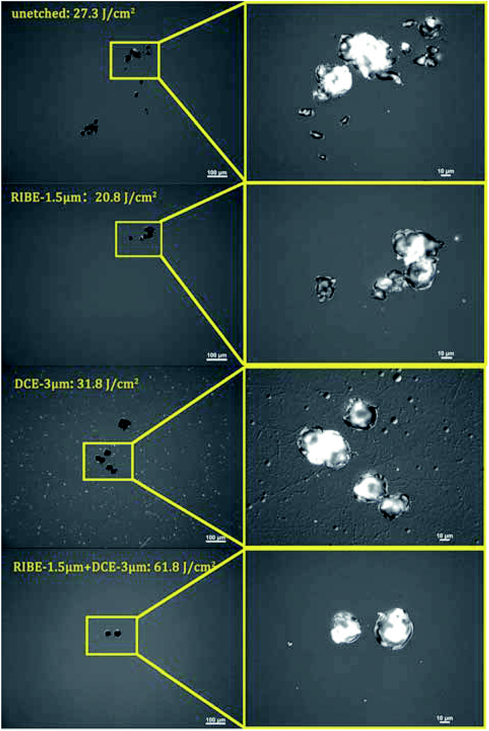 | ||
| Fig. 7 Laser damage morphology of the samples at their damage threshold of zero probability. | ||
A comparison of the damage sites morphologies of the samples with different etching processes suggests a change of damage mechanism (Fig. 8). Damage precursors in fused silica optics fabricated by conventional polishing process are confined within the subsurface layer, containing cracks that act as traps for various fractured defects and polishing compounds (on the left in Fig. 8). Chemical acid etching and careful cleaning have been demonstrated to be the most effective method for removing the SSD and improving the damage resistance of fused silica.27,28 However, deep chemical etching generally leads to the degradation of surface quality (upper part on the right in Fig. 8), which can enhance scattering and loss of laser beam energy. Optical field enhancement can readily occur on such microscopic defects, causing the reduction of laser-induced damage threshold.29 The deposition of reaction product (SiF62−) during the HF etching has been demonstrated to be a key challenge for realizing the best increase of LIDT.30 Ref. 25 also suggests that the presence of deteriorative bonding-structure on DCE-treated surface might be disadvantageous to improve the damage resistance of fused silica. We thus believe the HF-etched surface with large amounts of physical-structure defects (scratches or pits) have a high propensity for forming chemical-structure defects. The combined etching of RIBE and DCE considerably breaks the deadlock since the fractured defects that either absorb laser energy or cause field intensification can be effectively removed by the combined etching (lower part on the right in Fig. 8). Moreover, no physical-structure defects act as catalysts to inducing the formation of chemical-structure defects. Finally, the remarkable surface roughness (0.654 nm) obtained by the combined etching treatment is probably an underlying cause for realizing high damage threshold surface since the surface roughness values of the untreated and 3 μm DCE-treated samples (0.843 nm and 1.052 nm, respectively) were both higher than that of the sample treated by the combined etching process. In fact, there were still some stubborn scratches on the surface treated after the combined etching treatment and these faint features were difficult to be observed with optical microscopy. Therefore, we speculate that the combined process of RIBE and DCE could be further improved by increasing the RIBE depth or optimizing the relationship between physical bombardment and chemical reaction during the RIBE process.
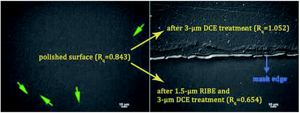 | ||
| Fig. 8 Comparison of etching morphologies of the samples. Left: the optical surface of the unetched sample. Polishing-introduced scratches were still faintly visible (marked with green arrowheads). Right: continual surface treated by single DCE (upper) and combined etching (lower). Mask (marked with blue arrowhead) was used to realize the two etching morphologies. The mean surface roughness (Rq) measured by white light interferometer for each sample is also given in the figures. Five testing points were randomly chosen for obtained the mean value. | ||
Conclusions
This study demonstrates that the LIDT of polished fused silica can be dramatically improved by combining RIBE with DCE technique. The best improvement in LIDT was achieved by using 1.5 μm RIBE pretreatment and 3 μm DCE retreatment. The ToF-SIMS results showed that RIBE-introduced impurities were effectively removed by the DCE treatment. An analysis of etching morphology showed that excellent surface quality (Rq = 0.654 nm) without microscopically visible scratches was obtained after the optical surface of fused silica undergoing the combined etching process. The results of this study suggest that RIBE treatment may be a valuable preprocessing tool for compensating the disadvantage of chemical etching of fused silica optics, especially in applications where conventional RIE treatment is not possible for uniformly modifying large-aperture and irregular optical surface.Conflicts of interest
There are no conflicts to declare.Acknowledgements
Authors gratefully acknowledge the financial support of National Natural Science Foundation of China (NSFC) (61705204 and 61705206), Development Foundation of China Academy of Engineering Physics (No. 2015B0403095), and Laser Fusion Research Center Funds for Young Talents. (No. LFRC-PD011). The authors would like to thank Jin Huang team for assistance in sample preparation and execution of the experiments. The authors are also grateful to Changpeng Li and Shufan Chen for helpful discussions.Notes and references
- J. A. Paisner, W. H. Lowdermilk, J. D. Boyes, M. S. Sorem and J. M. Soures, Fusion Eng. Des., 1999, 44, 23–33 CrossRef.
- X. Fortin, F. Garaude and B. Canaud, Nucl. Fusion, 2004, 44, 1118–1129 CrossRef.
- Q. Zhu, X. Wei, F. Jing, B. Feng, J. Wang, L. Liu and X. Deng, Proc. SPIE, 2013, 9266, 11306–11312 Search PubMed.
- P. E. Miller, J. D. Bude, T. I. Suratwala, N. Shen, T. A. Laurence, W. A. Steele, J. Menapace, M. D. Feit and L. L. Wong, Opt. Lett., 2010, 35, 2702–2704 CrossRef PubMed.
- X. Q. Guo, X. D. Jiang, J. Huang, F. R. Wang, H. J. Liu, X. Xiang, G. X. Yang, W. G. Zheng and X. T. Zu, Acta Phys. Sin.-Ch. Ed., 2006, 55, 1201–1206 Search PubMed.
- D. Guo, X. Jiang, J. Huang, F. Wang, H. Liu, X. Xiang, G. Yang, W. Zheng and X. Zu, Opt. Express, 2014, 22, 29020–29030 CrossRef PubMed.
- H. X. Deng, X. T. Zu, X. Xiang and K. Sun, Phys. Rev. Lett., 2010, 105, 113603 CrossRef PubMed.
- F. Dahmani, S. J. Burns, J. C. Lambropoulos, S. Papernov and A. W. Schmid, Opt. Lett., 1999, 24, 516–518 CrossRef PubMed.
- G. Hu, Y. Zhao, X. Liu, D. Li, Q. Xiao, K. Yi and J. Shao, Opt. Lett., 2013, 38, 2632–2635 CrossRef PubMed.
- T. I. Suratwala, P. E. Miller, J. D. Bude, W. A. Steele, N. Shen, M. V. Monticelli, M. D. Feit, T. A. Laurence, M. A. Norton, C. W. Carr and L. L. Wong, J. Am. Ceram. Soc., 2011, 92, 416–428 CrossRef.
- S. H. Baxamusa, P. E. Miller, L. L. Wong, R. Steele, N. Shen and J. D. Bude, Opt. Express, 2014, 22, 29568–29577 CrossRef PubMed.
- X. Ye, J. Huang, H. Liu, F. Geng, L. Sun, X. Jiang, W. Wu, L. Qiao, X. Zu and W. Zheng, Sci. Rep., 2016, 6, 31111 CrossRef PubMed.
- L. Wong, T. Suratwala, M. Feit, P. Miller and R. Steele, J. Non-Cryst. Solids, 2009, 355, 797–810 CrossRef.
- M. Feit, T. Suratwala, L. Wong, W. Steele, P. Miller and J. Bude, Proc. SPIE, 2009, 7504, 75040L CrossRef.
- L. Sun, H. Liu, J. Huang, X. Ye, H. Xia, Q. Li, X. Jiang, W. Wu, L. Yang and W. Zheng, Opt. Express, 2016, 24, 199–211 CrossRef PubMed.
- S. J. Fonash, J. Electrochem. Soc., 1990, 137, 3885–3892 CrossRef.
- L. Sun, J. Huang, H. Liu, X. Ye, J. Wu, X. Jiang, L. Yang, W. Zheng and W. Wu, Opt. Lett., 2016, 41, 4464–4467 CrossRef PubMed.
- C. W. Chung, S. S. Kim, S. H. Seo, H. Y. Chang and N. S. Yoon, J. Appl. Phys., 2000, 88, 1181–1183 CrossRef.
- K. C. Shaing and A. Y. Aydemir, Phys. Plasmas, 1997, 4, 3163–3166 CrossRef.
- Y. Fu, N. K. A. Bryan and O. N. Shing, Rev. Sci. Instrum., 2000, 71, 1009–1011 CrossRef.
- Y. Liu, D. Xu, X. Xu, Y. Hong and S. Fu, Proc. SPIE, 2007, 6724, 67240K CrossRef.
- T. Haensel, A. Schindler, A. Nickel, and H. J. Thomas, Optical Systems Design and Production, 1999, vol. 3739, pp. 167–175 Search PubMed.
- L. Sun, H. Jin, X. Ye, H. Liu, F. Wang, X. Jiang, W. Wu and W. Zheng, Optik, 2016, 127, 206–211 CrossRef.
- G. W. Gibson, Method and structure for controlling plasma uniformity, US Pat., US 6110395 A, 2000.
- L. Sun, J. Huang, T. Shao, X. Ye, Q. Li, X. Jiang, W. Wu, L. Yang and W. Zheng, Opt. Express, 2018, 26, 18006–18018 CrossRef PubMed.
- X. Fu, M. Commandré, L. Gallais, M. Mende, H. Ehlers and D. Ristau, Appl. Opt., 2014, 53, A392–A398 CrossRef PubMed.
- M. Pfiffer, P. Cormont, E. Fargin, B. Bousquet, M. Dussauze, S. Lambert and J. Néauport, Opt. Express, 2017, 25, 4607–4620 CrossRef PubMed.
- S. H. Baxamusa, P. E. Miller, L. L. Wong, R. Steele, N. Shen and J. D. Bude, Opt. Express, 2014, 22, 29568–29577 CrossRef PubMed.
- N. Bloembergen, IEEE J. Quantum Electron., 1974, 10, 375–386 CrossRef.
- T. I. Suratwala, P. E. Miller, J. D. Bude, W. A. Steele, N. Shen, M. V. Monticelli, M. D. Feit, T. A. Laurence, M. A. Norton, C. W. Carr and L. L. Wong, J. Am. Ceram. Soc., 2011, 92, 416–428 CrossRef.
| This journal is © The Royal Society of Chemistry 2018 |