
 Open Access Article
 This Open Access Article is licensed under a Creative Commons Attribution-Non Commercial 3.0 Unported Licence
Investigation of dual-bend serpentine/spiral waveguides coupled to a microchannel system for competent, evanescent-wave-absorption-based, on-chip, biological-/chemical-sensing applications†
Amit Prabhakar *ab,
Neha Mishrab,
Deepti Vermac and
Soumyo Mukherjia
*ab,
Neha Mishrab,
Deepti Vermac and
Soumyo Mukherjia
aDepartment of Biosciences and Bioengineering, IIT Bombay, Mumbai 400076, India. E-mail: amit@iiita.ac.in
bIndian Institute of Information Technology Allahabad, Deoghat, Jhalwa, Allahabad-211015, India
cDepartment of Chemistry, Magadh University, Bodhgaya-824234, India
First published on 17th October 2018
Abstract
U or C-shaped waveguides, coupled to analyte microchannels, have been shown to be very responsive to evanescent-wave-absorption-based sensing. However, due to only having a single C-bend length, for analyte interaction in earlier devices, there was always an opportunity to advance their evanescent-absorbance sensitivity, by including multiple C-bend structures (interfaced with the analyte microchannel system) in the device design. To achieve this objective, two different types of waveguide probes (having a different orientation of two C-bends), i.e. S-bend and spiral-bend, were theoretically analyzed and further, experimentally tested for their comparative sensitivity to evanescent wave absorption, in this pioneering study. A novel single-step fabrication procedure (using an SU-8 photoresist), was executed to fabricate these waveguide structures interfaced (both at their inner and outer bend surfaces) with a microchannel system, along with fiber-to-waveguide coupler structures. Experimentally, the sensitivity of the S-bend waveguides was found to be ∼25% higher compared to that of spiral waveguides of similar dimensions, which corroborated the results from numerical modeling. Compared to our earlier embedded C-bend waveguides, the overall evanescent-wave-absorption-based detection sensitivity of the embedded spiral and S-bend waveguides were found to be improved by ∼7.5 times and ∼9 times respectively. Finally, these devices were found to be ideally suited for more sensitive biological-, as well as, chemical-sensing applications, provided a suitable surface alteration process is performed to these waveguide probes. Further, the proposed device has a possible capability for: facile continuous (real-time) analysis, a fixed sample volume interaction, and control over the evaporation of analyte samples introduced in to the device.
1. Introduction
There are a large range of fiber-optic sensors that measure different properties of an analyte using a number of optical methods.1–4 Several researchers have tried to increase the sensitivity of these sensors by enhancing their evanescent-field-penetration depth, and generally, they have achieved it by bending5,6 or tapering7,8 the fiber probes, altering the light launching angle,9 and increasing the wavelength10 used for detection. Bending a uniformly de-cladded optical fiber is a comparatively easier method (considering the fabrication process) and is also an efficient way to enhance the evanescent field5,6 around these sensor probes. Higher order modes are created by the fiber bending, which results in the evanescent field having a greater penetration depth.5 The higher sensing ability of a U probe with similar dimensions (compared to a straight probe) was demonstrated in ref. 6 Here, the larger absorption coefficient for a U probe indicated that the U probe had a larger evanescent field.6 The decrease in the angle of propagation in U probes as compared to the constant angle of ray propagation in straight fiber probes effectively increases the penetration depth of the evanescent field. In another study, Littlejohn et al. demonstrated that heat-coiled de-cladded optical fiber sensors with more than one bend (of a larger bending diameter = 1 cm) are more sensitive compared to single-bend fiber probes.5 Calculations performed by Gupta et al.11 showed that lower bend-diameter bend waveguides are more sensitive for evanescent-field-absorbance-based sensing. However, the bending diameter used by Littlejohn et al.5 was greater than 1 cm. For optical fiber sensor probes, the creation of lower-bend-diameter (<1 mm) multiple-bend fiber-optic sensor probes is much more difficult compared to the construction of single-bend sensor probes. Although, these multiple-bend fibers provided higher sensitivity compared to single-bend sensor probes, they required a few milliliters of analyte solution to immerse the multiple bends of the sensor.5 This study aimed to fabricate embedded waveguide optical sensors, which could alleviate both the problems of the bend diameter and the large sample volume.In our earlier design, we interfaced only the outer bending surface of a U-shaped waveguide for detection purposes.12,13 Even though the U-shaped embedded waveguide probe was an efficient design for microfluidic applications, only a smaller length of the outer surface of the waveguide was used for sensing. Although, recently, a few other studies have reported U-shaped polymer waveguide probes;14 however, only a smaller length of waveguide surface was typically used for sensing. We comprehensively investigated the U-bend SU-8 waveguides (theoretically and experimentally), in our earlier reported study,15 and in a very recent study.16 The low surface area of interaction restricted the sensitivity of these U-bend-waveguide-based devices, which was barely sufficient for using them in any practical evanescent-wave-absorption-based biological-/chemical-sensing applications.
To enhance the sensitivity, the introduction of a multiple-bend structure may be considered as a decisive approach for a variety of sensor applications. However, to the best of our knowledge, an extensive theoretical and experimental analysis for dual-bend polymer waveguides has not been presented in any earlier studies. Siebert et al.17 and Han et al.18 presented an optical gas analysis sensor using a single-mode spiral optical waveguide working in the middle-infrared region. Lavchiev et al. also showed a sensor design based on a single-mode straight Si waveguide (WG) on a low refractive index Si3N4/SiOx/Si3N4 membrane, where the waveguide interacted with the fluid sample by means of the evanescent field that extended into the sample.19 However, these reported devices seemed to be not suitable for liquid analyte samples, because the designs did not contain suitable closed microchannel structures (around the waveguide sensor probe) allowing for placement of a constant volume of fluid samples to interface with the fixed length of waveguide during the detection process. Further, the absence of possible close microchannel structures may allow the liquid samples to evaporate, which may not ensure the concentration of sample is constant, leading to an irregular real-time output of the sensing device for similar concentrations. Further, the difficult optical alignment issue of these waveguides with a light source and optical transducer and complicated multi-step fabrication technique used for these device fabrication may cause the device to be more costly. In an another approach, Feidenhansl et al. reported a thiolene polymers-based device, where the microfluidic channels and optical waveguides were simultaneously created in one molding step.20 However, the study presented the device with a single-bend structure and did not explore the possibility of any dual-bend waveguide structures (spiral and S-bend waveguides), integrated with the microchannel, following its experimental and theoretical explanation. Further, the difficult fabrication technique used for the device fabrication may also cause the device to be costly. As a preview for improving the sensor design for liquid analyte samples and reducing the fabrication cost, two different evanescent-wave-absorption-based microfluidic analysis chips are proposed, and further, were theoretically and experimentally investigated for chemical- and biological-sensing applications in the present study.
In these design approaches, the waveguide probes fabricated had two bends, and the design utilized both the inner and outer surfaces of the waveguides (interfaced with the microchannel) for analyte sensing. Considering the way in which the two bends were oriented with respect to each other, they could be either S-shaped or spiral-shaped waveguides. In the case of embedded S-shaped waveguides, the two bends (each an individual C-bend) structures were oriented in opposite directions, while in the case of embedded spiral waveguides, the bends were oriented in the same direction in a spiral fashion.
2. Theoretical study
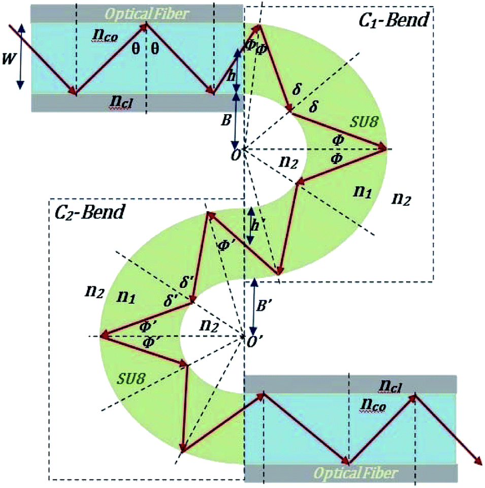
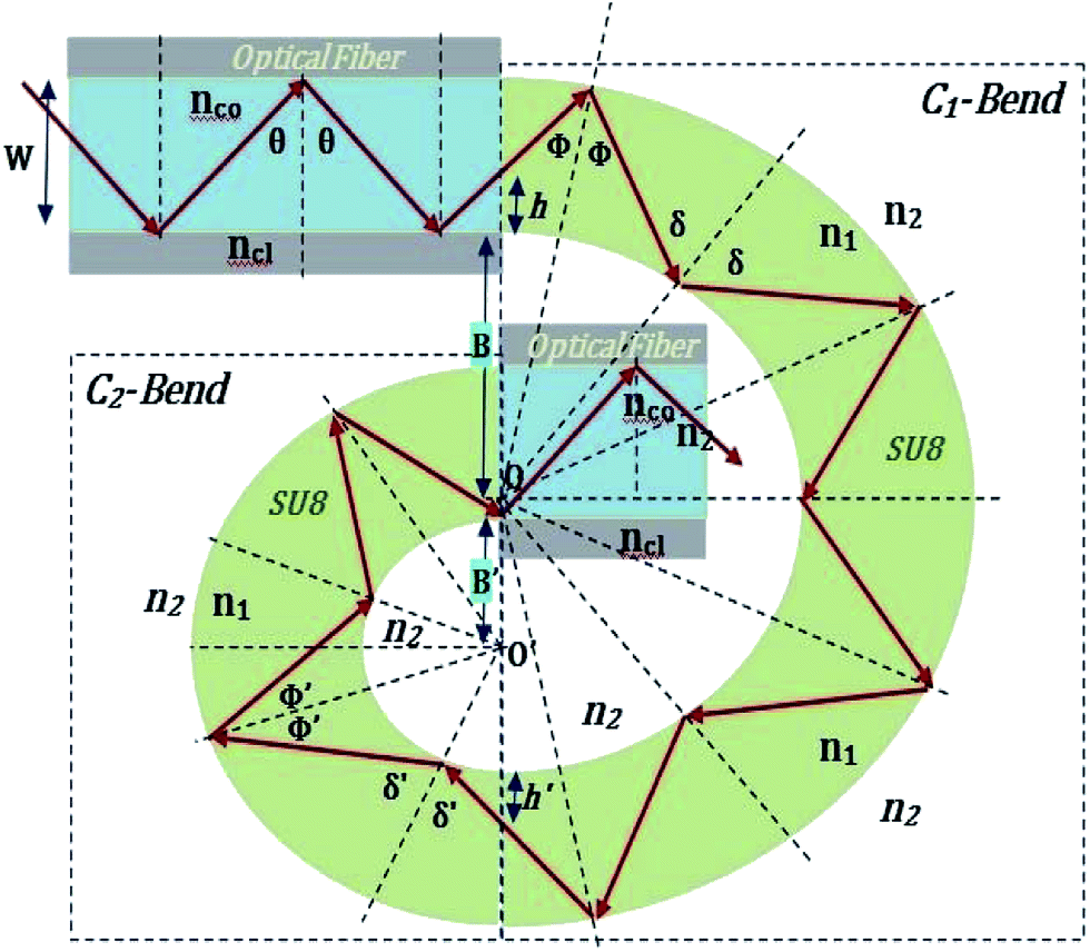
The guidance of the light beam through the SU8 waveguide took place because of the phenomenon of total internal reflection (TIR). The angle of incidence of traveling optical rays varies in between ∼39° (critical angle of SU8 for n1 = 1.59 and nclad = 1) to 90°, if all the bound rays are launched at the input end of the SU8 waveguide (from an optical fiber).15The S-bend or spiral waveguide consists of two C-bends. The first C-bend from the direction of input light is referred to as C1-bend and the next one as C2-bend.
2.1 Calculation of the range of angle of incidence for the S-bend waveguide
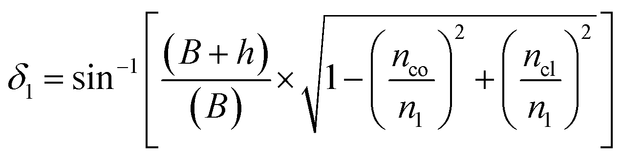
The critical angle of an optical fiber core can be given as:
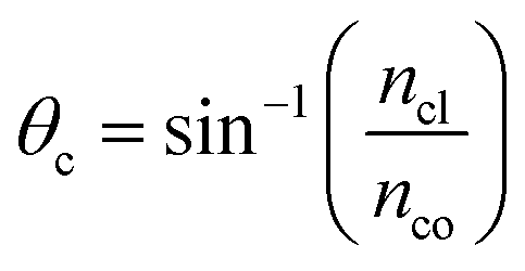 | (1) |
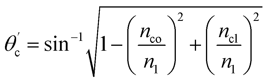
The range of angle of incidence θc (critical angle in the optical fiber core) to 90° (with the normal to the core cladding interface) in the optical fiber (coupled to the SU8 waveguide end) changes (as a ray enters the straight SU8 waveguide end), and it varies between 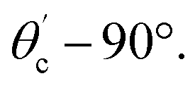
Values of the angle of incidence at the straight SU8 waveguide end can be calculated as follows (see the ESI†):
 | (2) |
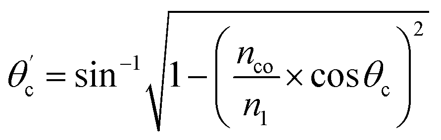
From eqn (1) and (2),  can be written as:
 | (3) |
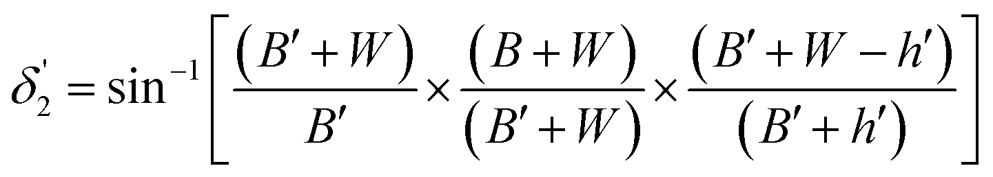
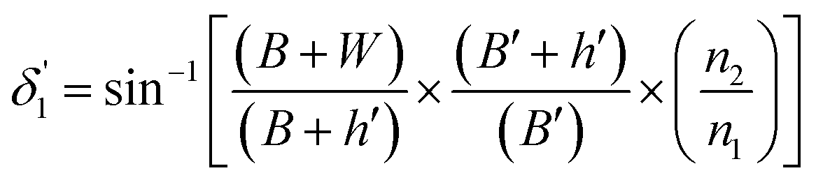
The range of angle of incidence  to 90° at the straight SU8 waveguide end (coupled to the first C-bend waveguide end) changes (as a ray enters the first C-bend waveguide), and it varies between Φ1–Φ2, at the outer bend surface, and δ1–δ2 at the inner bend surface (Fig. 1).
 | ||
| Fig. 1 Schematic of ray guidance in two of the U-bends of the embedded S-bend optical waveguide sensing probe. | ||
By modifying the calculation done by Gupta et al.,11 these angles can be written as (see the ESI†):
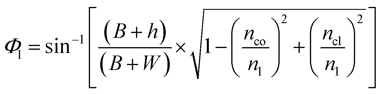 | (4) |
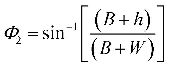 | (5) |
On the other hand:
 | (6) |
The range of angle of incidence Φ1 to Φ2 (with the normal to the core cladding interface) in the first C-bend (coupled to the second C-bend waveguide end) changes (as a ray enters the second C-bend waveguide), and it varies between  , at the outer bend surface, and
  at the inner bend surface (Fig. 1).
Values of the angle of incidence at the second C-bend can be calculated as follows (see the ESI†):
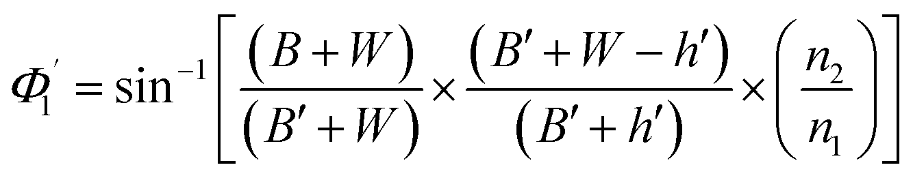 | (7) |
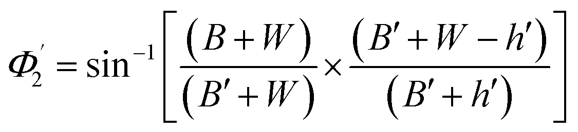 | (8) |
On the other hand:
 | (9) |
 | (10) |
2.2 Calculation of the range of angle of incidence for the spiral waveguide
The range of angle of incidence θc to 90° (to the normal to the core cladding interface) in the optical fiber (coupled to SU8 waveguide end) changes as a ray enters the straight SU8 waveguide (eqn (1)–(3)). The range of angle of incidence changes further as the ray enters the first C-bend waveguide, and it varies between Φ1–Φ2, at the outer bend surface, and δ1–δ2 at the inner bend surface. The value of Φ1–Φ2 and δ1–δ2 can be explained by eqn (4)–(6) given earlier.Further, the range of angle of incidence Φ1 to Φ2 (with the normal to the core cladding interface) at the first C-bend (coupled to second C-bend waveguide end) changes (as a ray enters the second C-bend waveguide), and it varies between  , at the outer bend surface, and
 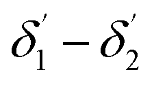 at the inner bend surface (Fig. 2).
 | ||
| Fig. 2 Schematic of ray guidance in two of the C-bends of the embedded spiral-bend optical waveguide sensing probe. | ||
Values of the angle of incidence at the second C-bend can be calculated as follows (see the ESI†):
 | (11) |
 | (12) |
On the other hand:
 | (13) |
 | (14) |
As the waveguide is interfacing with the microchannel (analytes) with its outer as well as inner bend surfaces, so for all the numerical explanations, both (the inner and outer bend) surfaces of both the C-bend waveguides were considered.
2.3 Fractional losses due to the total internal reflection
A specific amount of optical energy is lost during the total internal reflection (TIR) of rays that are incident to the interface of the core and cladding (optically absorbing) at angles greater than the critical angle. There can be multiple reflections of these rays – all incident rays with a specific angle to the outer/inner surfaces of the two bent regions. As discussed by Snyder et al.,21 the fractional loss of these propagating rays at the outer (Lo) or inner bend surface (Li) due to each of the TIRs was explained in our earlier studies15 as follows:
 | (15) |
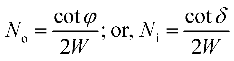
The number of ray reflections per unit length at each outer (No) or inner (Ni) bend surface of the C-shaped sensing region and its relation with the angle of incidence of incident rays Φ or δ (with the normal to the core cladding interface) at the outer or inner bend surfaces and the width of the waveguide (W) can be written as:11
 | (16) |
The determination of the fractional loss of optical power per unit length (LN) of the semicircular (C-shaped) waveguide was explained in our earlier studies.15 It can be determined by multiplying the corresponding L and N values for the inner and outer bend surfaces, i.e.
| LN = Lo × No, or LN = Li × Ni | (17) |
Integrating LN for higher (ψ2 = π/2 − φ2) and lower (ψ1 = π/2 − φ1) range values angles of incidence at the waveguide surface gives:
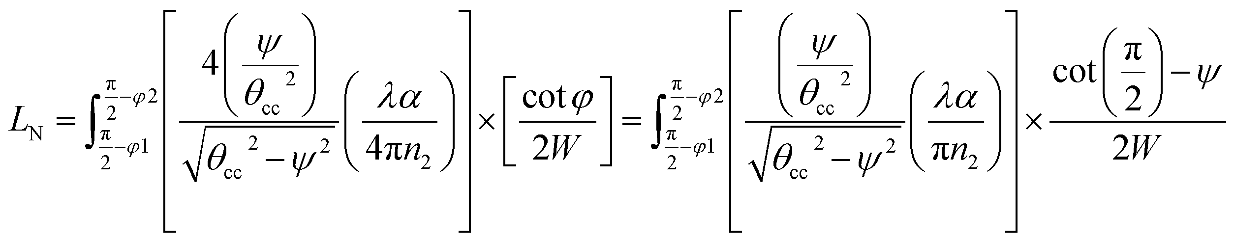 | (18) |
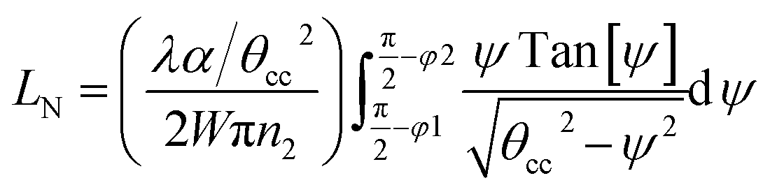 | (19) |
For embedded S-bend waveguides, eqn (4)–(6) were used to calculate the incidence angle ranges at the outer (Φ1–Φ2) and inner surfaces (δ1–δ2) of the first C1-bend region, with eqn (7)–(10) used to calculate the incidence angle ranges at the outer  and inner surfaces
  of the second C2-bend region. For embedded spiral-bend waveguides, eqn (4)–(6) were used to calculate the incidence angle ranges at the outer (Φ1–Φ2) and inner surfaces (δ1–δ2) of the first C1-bend region, and eqn (11)–(14) were used to calculate the incidence angle ranges at the outer
 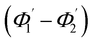 and inner bend surfaces
  of the second C2-bend region. All the h and h′ values (between h or h′ = 0, to h or h′ = W) were considered for calculating these values. The minimum and maximum values of incidence angles at the inner/outer bend surface of both the U-bend surface of embedded S-bend and spiral-bend waveguides are presented in Tables 1s and 2s, respectively (of the ESI†). However, it is obvious that (due to the higher critical angle of optical fibers) higher the order modes from SU8 waveguide 2nd bend will not couple back to the receiving fiber end. So the angles of incidence of the modes that can travel in 2 bends of the SU8 waveguides as well as in the receiving optical fiber end are given as
  and
and  in Tables 1s and 2s of the ESI.†
The loss of optical power per unit length (LN) was calculated (using eqn (19)) at the fixed values of W = 200 μm, ε = ∼8 μ−1 M−1 (extinction coefficient for methylene blue at 0.625 μ wavelength), λ = 0.625μ and θcc = 33° (for n2 = 1.33 of D.I. water). For different concentration values of methylene blue solution, their corresponding absorption coefficients (α in μ−1) was calculated by multiplying its extinction coefficient (ε) with their molar concentration (M). Upper  and lower limit
  values (i.e. the complementary angles of the minimum and maximum values of the angles of incidences Φ or δ) were put in to the eqn (19) to calculate the LN values for the C1 and C2 bends of S-bend/spiral waveguides. The total loss due to all the TIRs was calculated by multiplying the LN value with the corresponding equal interaction lengths (i.e. bending periphery) of the different bending radius (B) of the C1/C2-bends of the S-bend and spiral-bend waveguides.
The calculated values of the absorbance with respect to the increasing values of methylene blue concentration for S-bend and spiral waveguides are presented in Fig. S3 (in sub-section 4 of ESI†). The calculations revealed that the total fractional loss due to all the TIRs (at a particular analyte absorption coefficient (α) value) was ∼22% higher in the case of the S-bend waveguide compared to spiral-bend waveguides. This may be due to the comparatively steeper change in the angle of incidences of rays when they pass from the C1-bend to the C2-bend of S-bend waveguides. The ray optics model chosen by us to explain our sensor's sensitivity may not be absolutely sufficient for this type of sensor; however, we assumed that because of its simplicity and ease of calculation, the presented model may prove to be an alternative simple tool to predict the probable sensitivity.
2.4 Methylene blue as an analyte
The suitability of these devices for analytical purposes was demonstrated by evanescent wave absorption measurements with methylene blue solution as an analyte. We were preferably interested in utilizing the proposed device for efficient biosensing applications. The selection of methylene blue dye molecule for our initial experiments was due to the fact that the adsorption of positively charged methylene blue molecules over the negatively charged SU8 surfaces has comparable reaction kinetics to receptor-analyte binding kinetics. It also helped in reducing the cross-coupling effect,16 which is a relatively un-wanted effect for pure evanescent-absorbance-based sensing. The detailed reason for the selection of this dye molecule for the experiments is explained in sub-section 5 of the ESI.† The comparative sensitivity of single-bend embedded waveguide probes for methylene blue and FITC-tagged GaHIgG as analyte molecules is also explained in sub-section 6 of the ESI.† However, other non-adsorbing analyte molecules, i.e., CoCl2 dissolved in isopropyl alcohol, may also be used as a test fluid for this device.3. Design and fabrication
Using the mask design (explained in Fig. 3a and b), the SU8 layer was patterned into two side-by-side S-shaped microchannels, each 200 μm wide and partitioned by an integrated S-bend waveguide of 200 μm width, an inlet/outlet reservoir, and two identical “fiber-to-waveguide coupler” structures (Fig. 3a and b). | ||
| Fig. 3 (a) Mask design of device comprising a microchannel, S-bend waveguide, and optical fiber coupler structure. (b) Close-up look of the microchannel interfacing with the S-bend waveguide. (c) Mask design of the device comprising a spiral microchannel, spiral waveguide, and optical fiber coupler structure. | ||
In the case of the embedded spiral waveguide, the SU8 layer was patterned into a spiral microchannel, outlined by the side walls of the integrated spiral waveguides (with inlet and outlet reservoirs) and two different tapered grooved fiber-to-waveguide coupler structures (Fig. 3c). Here, the mask design comprised a 200 μm width spiral waveguide (Fig. 3c) with two U-shaped turns of different bending diameters. In spite of the other design constraint, i.e., integration of the microchannel and fiber-to-waveguide coupler structure, both types of dual-bend waveguides were intended to be designed with a minimum possible bending radius. The smaller and larger bends of the spiral waveguide (width = 200 μm) were assigned 1.5 mm and 2 mm bending diameters, respectively; however, both the bends of the serpentine waveguide (width = 200 μm) were assigned 1.5 mm bending diameter. The effect of lowering the U-bend waveguide's bending radius on its sensitivity was previously extensively investigated in our earlier report on embedded U-bend waveguides.15
The overall waveguide lengths of both the S-bend and spiral-bend device were taken as ∼4 cm. These waveguides acted as side walls of the 200 μm width microchannel that shaped the microchannel into a spiral form.
The reason for opting for this waveguide cross-section and bending diameter was purely based on our earlier experience4,5,14,15 and the requirements for making an effective microfluidic device having an optimum waveguide propagation loss and sufficient mechanical strength able to withstand the microchannel bonding/sealing process (Fig. 4b). The device's microfluidic structure is also expected to sustain fluid shear stress, excreted on the microchannel walls (which also consist the waveguide inner/outer bend surfaces), while the fluid is flowing. During the design of the device, care was also taken care that the waveguide-embedded microchannel should be continuous and without any micro-packets, which may cause air entrapment during flow of the analyte solution in the device, as this could cause unpredictable changes in absorbance (measured via our given experimental setup; Fig. 6) during introduction of the analyte solution.
 | ||
| Fig. 4 Fabrication procedure for SU8 waveguide-embedded, microfluidic system (a) SU8 microstructure after photolithography (i.e., after, RCA cleaning, wet oxidation and dehydration bake of the silicon wafer; followed by SU8 spin-coating over the silicon wafer; its pre-exposure bake, exposure, post-exposure bake, and its final development using the SU8 developer); (b) spin-coating of PDMS on PMMA lid, semi-cured and pressed against the SU-8 open pattern of the microchannel, followed by closing the microchannel and curing for another 1 h at 70 °C; (c) attachment of the outlet and inlet tubing in the respective reservoirs; (d) minute schematic details of the reservoir at inlet and outlet ends. (1): SU8 waveguide for coupling light input/output; (2): SU8 waveguide (straight terminal part of S-bend design); (3): microchannel SU8 side walls; (4): reservoir SU8 side walls; (5): patterened SU8 reservoir with dividing waveguide (reservoir lower section); (6): through hole in PMMA lid (reservoir upper section); (7): PMMA lid; (8): analyte flow; (9): substrate (SiO2). | ||
 | ||
| Fig. 5 (a) Schematic diagram of the embedded spiral waveguide device, (b) schematic for attachment of the outlet and inlet tubing and optical fiber with the embedded spiral waveguide device. | ||
 | ||
| Fig. 6 Schematic view of the experimental setup for embedded S-bend waveguides. | ||
Similar to our design scheme reported earlier,12,13 two tapered, open-ended grooves (i.e., fiber-to-waveguide coupler structures) were incorporated in the design to couple the LED source and spectrophotometer to the S-bend waveguide's endings through two optical fibers, respectively. In the case of the embedded spiral waveguide, due to the design requirement, one of the waveguide coupler structures was made closed ended (Fig. 3c).
The microfabricated, SU8, S-bend/spiral microchannel pattern (embedding the waveguide) (Fig. 4a) were sealed with a PMMA sheet (Fig. 4b) using PDMS as an intermediate adhesive layer, and finally the inlet and outlet tubing was attached (Fig. 4c). Before sealing the microchannel, the PMMA sheet (of 0.5 mm thickness) was holed at two points, for the inlet/outlet reservoirs of the S-bend/spiral microchannel (Fig. 4b and 5a). In the case of the embedded spiral waveguide, an extra third hole was made for the closed ended fiber coupler structure (Fig. 5a). For placing the optical fiber in the closed ended fiber-to-waveguide coupler structure of the spiral waveguides, the fiber was inserted inside the hole created in the PMMA sheet for this end and pushed further ahead, to couple it with the waveguide end (Fig. 5b).
At first look, it seems quite obvious that there is a geometrical difference between the design of the fabricated spiral waveguide (Fig. 3c) device (which was experimentally studied) and the schematic diagram for the theoretical study (Fig. 2), in terms of the difference in an additional straight waveguide section in between the C1- and C2-bends of the spiral waveguide (Fig. 3c). The device was designed in this way so that the microchannel and fiber coupler structures could be appropriately integrated with the spiral-bend waveguide. Theoretically, the presence of this additional straight waveguide section in the actual device (Fig. 3c and 5) do not contribute to any change in the range of angle of incidence when the incident ray travels from its C1-bend (where it varies between Φ1–Φ2) to C2-bend (where it varies between  ) of the spiral waveguide (similar to Fig. 2), via this straight waveguide. This is because of the fact that, as the light-ray travels from the C1-bend to the straight waveguide of device (Fig. 3c), the range of angle of incidence does not change much (i.e., it remains in between Φ1 and Φ2); further, as the rays enter from the straight waveguide section to the C2-bend waveguide the range of angle of incidence may change to a similar range (i.e., it may vary between
  and
and  ), as if the ray is entering directly from the C1-bend to the C2-bend of the spiral waveguide (as presented in Fig. 2). Considering these facts, we realized that we can explain the design of the device (Fig. 3c and 5b) via the schematic diagram as presented in Fig. 2 (i.e., both are anticipated to be theoretically equivalent).
4. Experimental results and discussion
The experimental setup for all the optical measurements with embedded S-bend/spiral waveguides is explained in Fig. 6. A red LED (Edison Opto, Taiwan) of 1 Watt power was used as the light source and a spectrophotometer (Ocean Optics Model, USB4000) was used as the detector in this case. Because of the two oppositely directed U-bend portions of the S-bend waveguides probe and the greater increment in the angle of incidence of light rays traveling from the first bend to the second bend, the loss of optical power is greater in the S-bend/spiral SU8 waveguides. Owing to the greater propagation loss of optical power in the lower wavelength region, in SU8 waveguides, a high power red LED (λmax = 620–640 nm) of 1 Watt power was used for all the experiments. Two plastic/polymer-clad silica optical fibers (core: 200 μm and length: 10 cm) were used for coupling the light (for the fabricated device, Fig. 6), from the light source and the spectrophotometer, respectively. The details regarding the methodology for measuring the coupling loss between the optical fiber and the SU8 waveguide, and experimentally measured coupling efficiency from fiber to waveguide and waveguide to fiber have already been explained in our recent publication.16 In the present device, a similar extent of coupling losses was observed as reported earlier.16As convention, D.I. water was taken as the reference for all the optical measurements of evanescent wave absorbance. Different concentrations of methylene blue (MB) dye solution (as analyte) were injected into the inlet tubing of the microfluidic system, embedded with the S-bend waveguide, which conducted the dye solution in to two S-shaped microfluidic channels (width = 200 μm), (arranged in parallel, on both sides of the S-shaped waveguide), and the corresponding absorbance readings were recorded (Fig. 7).
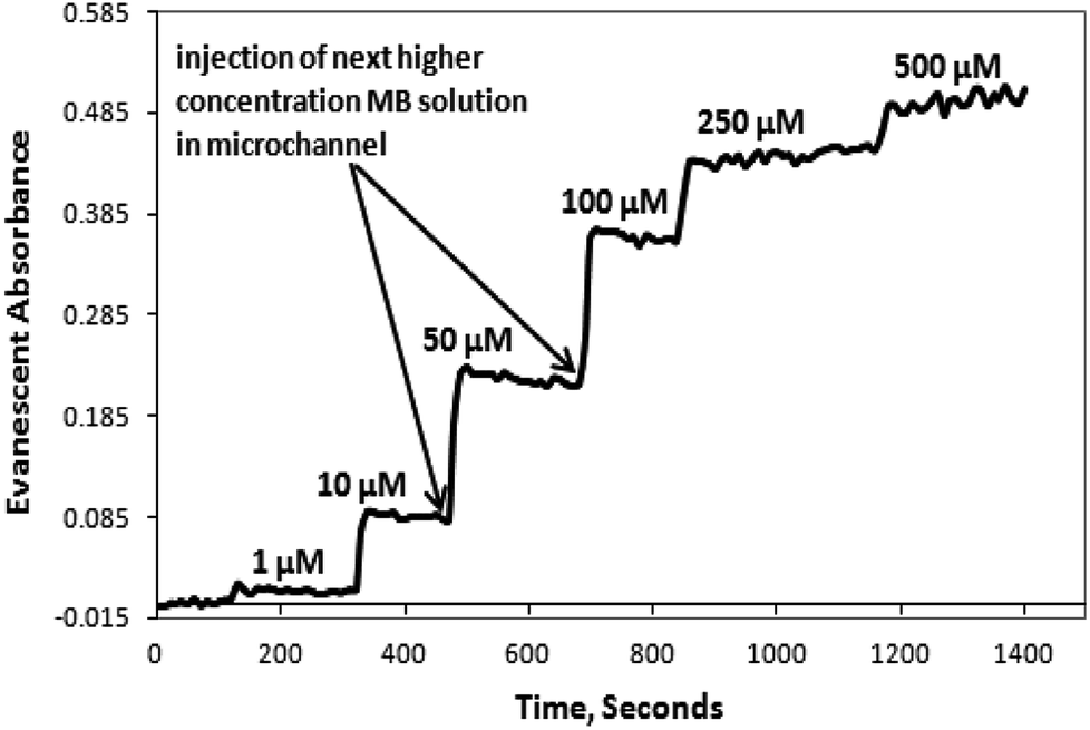 | ||
| Fig. 7 Evanescent wave absorbance vs. time (s) response of embedded S-bends waveguide after injecting different concentrations of methylene blue in the microchannel. The sudden rise region of the graph shows the injection of the next higher concentration methylene blue (MB) solution in the microchannel. | ||
In all of our measurements, we gently placed ∼0.1 mL (approximately) of analyte (MB) solution in to the microchannel system of the fabricated device, via a normal disposable syringe, and filled the microchannel, completely. Further, the measurement process was performed as described in our earlier studies.15,16
The present device design (Fig. 3 and 5), and the aforementioned microchannel filling method allowed the interaction of a fixed microchannel volume of analyte solution with a fixed length of dual-bend waveguides. Additionally, the possible closed/sealed microchannel system with a PMMA sheet (Fig. 4c and d and 5), also ensures that the liquid samples are not allowed to evaporate, which might ensure the concentration of the analyte sample to be constant during the measurements, leading to a constant real-time absorbance output of the sensing device for the similar concentrations. This represents a possible solution for the similar aforesaid problems that appeared in one of our earlier approaches.16 Further, considering the method of sample introduction, the effect of the flow rate (of each analyte, MB-solution during the measurements), on the device sensitivities, seemed to not be an issue in our experimental measurements.
In the case of the embedded spiral waveguide, the inlet tubing conducted the solution in to a single coupled spiral microchannel and the corresponding absorbance readings were taken. Fig. 7 displays the real-time absorbance change, with respect to the change in concentration of the MB dye solution introduced inside the microchannel for the embedded S-bend waveguide-based devices.
The microchannel system was flushed with D.I. water after each set of measurements for the different dye solutions, and the absorption spectrum was obtained. The S-shaped microchannel system integrated with the S-shaped waveguide was filled with water, and dark and light references (Fig. 8(1)) were taken, and later the microchannel system was filled with 500 μM concentration of methylene blue solution, and the intensity vs. wavelength graph (Fig. 8(2)) was obtained. Further, the microchannels were flushed with D.I. water and the intensity vs. wavelength graph (Fig. 8(3)) was obtained again. A comparison of this spectrum with the spectrum taken before the injection of dye, and that taken with 500 μM dye (Fig. 8) showed that there was some residual absorption of the dye molecule on the waveguide surface at the end. The detection limit of methylene blue solution for a described S-bend/spiral waveguide detection length with the experimental setup described was 1 μM.
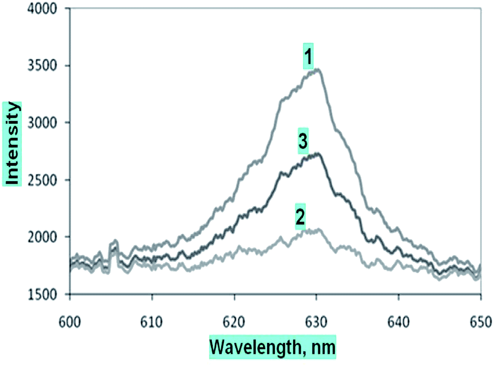 | ||
| Fig. 8 Intensity vs. wavelength graph obtained with the embedded S-bend waveguide, for (1) D.I. water, (2) 500 μM methylene blue, and (3) flushing 500 μM methylene blue (MB) filled channel with D.I. water solution, introduced inside the microchannel for the embedded S-bend and spiral waveguides, respectively. | ||
Fig. 9 shows a calibration curve for methylene blue (MB) solutions, at 625 nm. As expected, there is the initial quick rise in absorbance followed by a somewhat slower rise at higher concentrations. In the presented device design, the SU8 waveguide core was covered by a homogeneous liquid cladding containing a certain concentration of analyte molecules to be detected (Fig. 3, 5, and 6). For characterizing these devices, we used methylene blue solutions, which have SU8 waveguide surface adsorbing property; hence the light absorption across the waveguide revealed the hysteresis effect (i.e., the response of these devices for a certain concentration of analyte relied not only on the present concentration of that analyte but also on the previous history of that analyte concentrations that interacted with the device). The reason for selecting methylene blue as the analyte and the physical reason behind the adsorption are explained in Section 6 of the ESI.† However, any other analyte molecules which do not have an adsorption property with the SU8 waveguide surface may also be analyzed with this device, which will definitely not exhibit any hysteresis effect; hence, theoretically this effect is not always exhibited by this device.
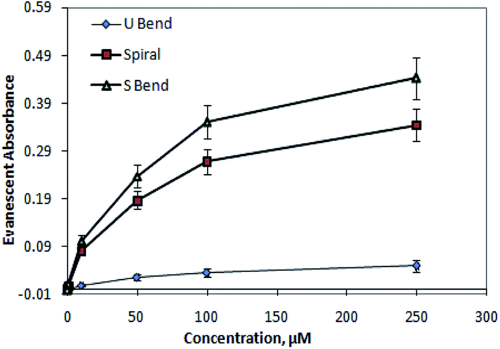 | ||
| Fig. 9 Comparative calibration curve of methylene blue solutions at 625 nm for embedded (1) outer bend surface U-bend waveguides, (2) spiral, and (3) S-bend waveguide. | ||
According to the experimental results, S-bend waveguides were found to be ∼25% higher in sensitivity compared to that of the similar dimension spiral waveguides. These findings corroborate the numerical calculation results. Compared to embedded U-bend waveguides, the overall evanescent-wave-absorption-based detection sensitivity of embedded spiral and S-bend waveguides were improved by ∼7 times and ∼9 times, respectively.
The experimentally measured values of absorbance (Fig. 9) were found to be higher compared to the calculated values shown in Fig. S3 (of the ESI†). This may be explained by the fact that, in the experimental absorbance measurements, a whole inner/outer bend surface area of the waveguide was considered; however, in the absorbance calculations only the length of the waveguide was considered (i.e., not its area).
For making both the experimental and calculation data equivalent, the experimentally measured absorbance values could be modified in terms of absorbance value per unit waveguide thickness. This proposed parameter was calculated (Fig. 10) by numerically dividing the experimental absorbance values (of the corresponding M-Blue concentration) with the waveguide thickness (i.e., 200 μm). The order of magnitude of this new parameter (i.e., absorbance value per unit micrometer thickness of the waveguide) was found to be quite similar with the calculated absorbance value (Fig. S3 (of ESI†) & 10).
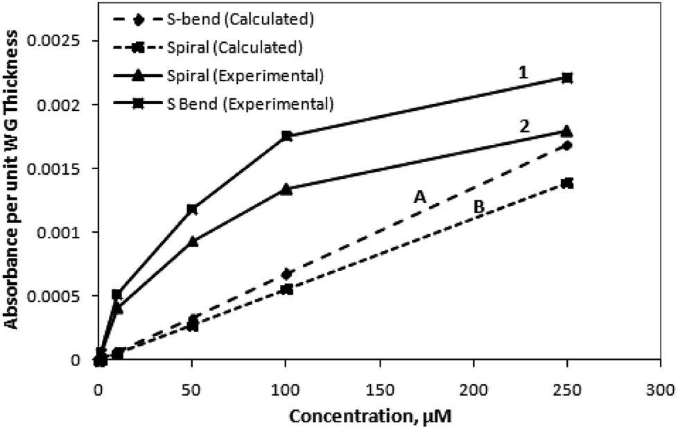 | ||
| Fig. 10 Calibration curve of absorbance value per unit micrometer of waveguide (WG) thickness (AU μ−1) vs. concentration for methylene blue at 625 nm for embedded (1) S-bend and (2) spiral waveguide. The experimental value is compared with the calculated values of the (A) S-bend waveguide and (B) spiral waveguide. | ||
Compared to the calculated calibration curve, the experimental curve (Fig. 9 and 10) of methylene blue (i.e., its absorbance at 625 nm vs. concentration) is nonlinear. This indicates an initial quick rise in absorbance at lower concentration, followed by a slower rise at higher concentrations. This loss of linearity at higher concentration is due to adsorption of charged methylene blue dye molecules on the SU8 waveguide. This concurs with evidence collected by earlier researchers6 and may be ascribed to a relatively higher rate of adsorption due to low stearic hindrance forces on the surface at lower concentrations. The intensity vs. wavelength graph (Fig. 8) also indicates the small amount of residual adsorbed dye molecule over the waveguide surface even after flushing the injected higher concentration dye solution with D.I. water at the end of each set of experiments. We did not use ethanol and other organic solvents for the washing of waveguide surface in our experiments as these could distort the structural integrity of these SU8 polymer-based device structures.
The higher experimental absorbance value for the lower methylene blue concentrations (compared to the calculated values) can be attributed due to the fact that, in our calculations (Fig. 10), the absorbance value per unit micrometer thickness of the waveguide, was considered. However, considering a 625 nm wavelength of propagating light, the possible value may lie in between these aforesaid absorbance values, and the absorbance value per unit nanometer thickness of the waveguide. Considering this information, both the experimental and calculated values may effectively approach each other.
The nonlinearity issue definitely restricts the usage of the given sensor probe for the evanescent-absorption-based detection of molecules that have an adsorption property with SU8 polymer-based waveguide microstructures. Hence, during a few of our earlier experiments, to minimize this adsorption effect, we tried to implement the flow of an organic washing solvent (i.e., ethanol), for cleaning the waveguide surface, in between the inflow of the experimental analyte solutions (i.e., the aforementioned various concentration of methylene blue solutions). However, during the continuous flow of the above-mentioned organic washing solvents, a leakage in the enclosing microchannel structure was observed quite often. These disturbances in the structural integrity of the device may be explained in the following way:
The devices include different polymer structures/entities, i.e., SU8 polymer (for waveguides, microchannel network, and waveguide couplers, microstructures); SiO2 deposited over silicon (as a substrate for patterning SU8 microstructures as well as the waveguide's lower cladding of the SU8 waveguide); PMMA polymer sheet (for enclosing the open microfabricated SU8 microchannel structure); PDMS thin layer (as an adhesive layer in between PMMA sheet and SU8 microstructures, for enclosing the open microchannel network); polypropylene tubing (as an inlet and outlet tubing attached to the PMMA sheet's inlet & outlet reservoir/opening for inflow and out-flow of the sample fluid through the given devices); and epoxy glue (for making an aforesaid bond between the polypropylene tubing and PMMA polymer sheet).
Possibly, the aforementioned leakage in the enclosing microchannel structure during the continuous flow of organic washing solvents may be due to the distortion of any of the aforementioned polymer-based structures/entities or a loosening of bonds between any two of the aforesaid device components (i.e., the bonds between: [1] SiO2 substrate & SU-8 microstructures; [2] PMMA-sheet/PDMS-polymer adhesive layer & SU8 microstructures; [3] polypropylene tubing & PMMA sheet's inlet & outlet reservoir/opening etc.), due to their interaction of organic solvent molecules.
However, to visualize the M-Blue adsorption effect on these SU8 polymer-based waveguide microstructures, we performed the experiments with a very limited flow of organic washing solvent (i.e., ethanol, for cleaning the waveguide surface), in between the inflow of experimental analyte fluids (i.e., the aforementioned various concentration of methylene blue solutions). Further, after the observation of the respective absorbance reading (and converting it in terms of the absorbance value per unit micrometer of waveguide thickness), a calibration curve was obtained and is presented in Fig. 11. The observation (Fig. 11) definitely indicates the improvement in the earlier linearity issues (Fig. 9 and 10), pertaining to the devices at higher concentration, considering the fact that only an extremely limited inflow of organic washing solvent was allowed, which could disturb the structural integrity of the device.
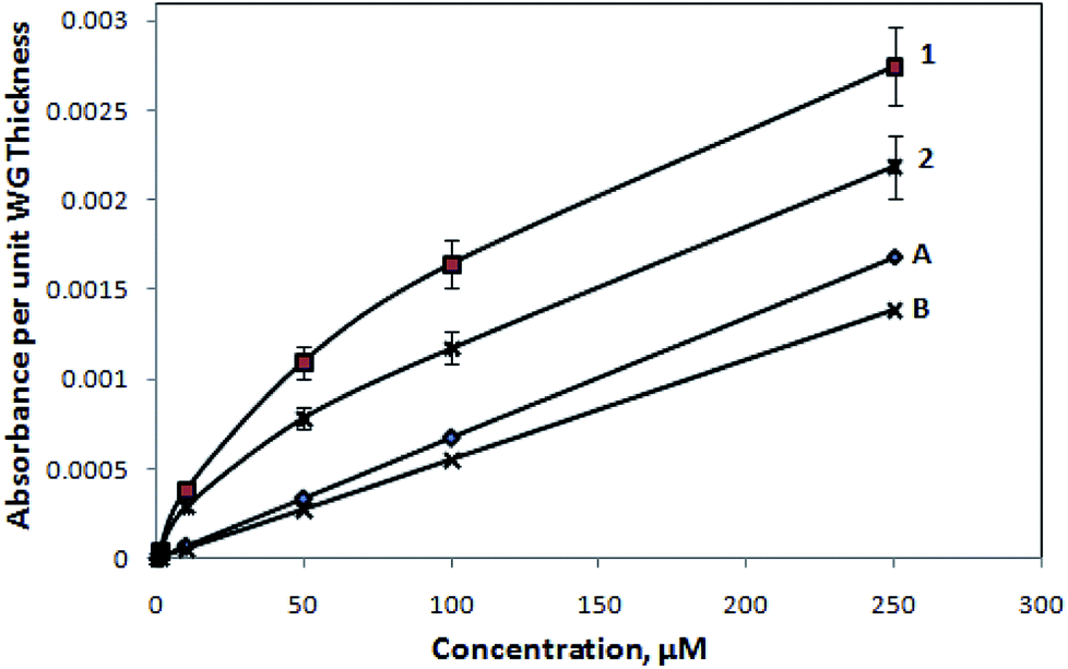 | ||
| Fig. 11 Calibration curve of absorbance value per unit waveguide (WG) thickness (AU μ−1) vs. concentration for methylene blue at 625 nm for embedded (1) S-bend and (2) spiral waveguide. The experiments were performed, with a very limited flow of organic washing solvent (i.e., ethanol, for cleaning the waveguide surface) in between the inflow of the aforementioned various concentration of methylene blue solutions. The experimental value is further compared with calculated values of (A) S-bend waveguide and (B) spiral waveguide. | ||
The embedded dual-bend waveguide-based sensors explained in this paper have ∼8 times higher surface area compared to embedded C-bend waveguides.15 So these sensors are expected to have ∼8 times higher methylene blue binding sites due to the SbF6− photoinitiator (view ESI†) compared to embedded C-shaped waveguides.15 Furthermore, due to the increase in length (i.e., increase in volume) of the microchannel, the number of moles of analyte introduced in to microchannel is 8 times higher compared to U-bend waveguides. Due to the larger surface area of the waveguide as well as its larger microchannel volume for analyte introduction (i.e., higher moles of interacting analyte molecule), similar concentrations of analyte may induce larger evanescent-absorbance changes in dual-bend waveguides (compared to single-bend waveguides). All these factors indicate a possible higher sensitivity of these embedded dual-bend waveguides. Experiments with methylene blue analyte also proved an average of ∼8 fold higher sensitivity of embedded dual-bend waveguides. Biosensing experiments on dual-bends waveguide are also expected to give a lower limit of detection (i.e., <1 μg mL−1) compared to single-bend waveguides (i.e., <7 μg mL−1). However, due to higher absorption coefficient of SU8 polymer material in 485 nm wavelength (which is the λmax for FITC-tagged GaHIgG molecules) and longer path length in dual-bend SU8 waveguides, the propagation and absorption losses in these embedded dual-bend (S-bend/spiral) waveguides are higher compared to the U-bend waveguides. Subsequently, the light output (with 1 Watt white LED optical power input) at the dual-bend waveguide end was feeble and noisy at 485 nm. Hence, experimentation and interpretation of the results were very difficult. However, these embedded waveguides were expected to work more effectively if longer wavelengths (red) were used. This suggest that, for the biosensing applications, bio-analytes labeled with red dye molecules (λmax = 615–640 nm) may be used. These dyes labels can be Alexa Fluor 633, m Cherry, Q Dot 605, Texas Red, or YOYO-3.
Our theoretical and experimental studies strongly indicated that the introduction of a second bend structure definitely helps in making a more sensitive sensor. However, once light has been coupled to a dual-bend waveguide for higher order modes, the waveguide length and waveguide propagation loss are the more important parameters affecting light loss in these waveguides. Because of these facts, we were unable to find any useful results with the experimental setup we used in our earlier studies,4,5,14,15 i.e., with a white LED (Edison Opto, Taiwan) of 1 Watt power as the light source and using a spectrophotometer (Ocean Optics Model, USB4000) as a detector. This is because of the over 76% average propagation loss for all frequencies of white light used in the experiments. Hence, we used a red LED (Edison Opto, Taiwan) of 1 Watt power in place of the white LED, which helped in reducing the fractional propagation loses due to scattering that occur during the propagation of light in these dual-bend SU8 waveguides. In spite of these facts, compared to embedded U-bend waveguides, the overall evanescent-wave-absorption-based detection sensitivity of embedded spiral and s-shaped waveguides were improved by ∼7 times and ∼9 times, respectively. Additionally, simply introducing more bends in the waveguide structure increased the waveguide length, unless the radius is correspondingly reduced, which may also affect the coupling to higher order modes. Considering these facts, we kept the radius of the second bend of the dual-bend waveguide either of the same dimension (i.e., for serpentine, Fig. 3a) or only slightly lower compared to its first bend (i.e., for spiral waveguides, Fig. 3b). As expected, these designs resulted in an increased waveguide length and consequently increased light propagation loss. To slightly overcome these issues, as mentioned above, a red LED was used in place of white LED.
5. Biosensing experiments with Alexa Fluor®633-tagged GaHIgG biomolecules
To investigate the capability of the microchannel embedded S-bend/spiral-waveguide-based devices for biosensing relevance, the bioreceptor–analyte pair of: IgG–Anti IgG was used. The presented embedded S-bend waveguides, which have higher overall sensitivity, were selected for the experiment, and were immobilized with bioreceptor (HIgG) molecules, performing the procedure elucidated by Deepu et al.22 This is usually executed via chemical modification of the SU8 surface initially by the serial injection of NaOH solution, HCl solution, glycine solution, and finally EDC: NHS solution in to the dual microchannels embedded with the S-bend waveguide and maintaining there for a given period. Additionally, the solution of antibody: human IgG (HIgG) was introduced in to the microchannel and reserved overnight for their immobilization on to the side surfaces of the SU8 polymer-based S-bend waveguide, interfacing with the microchannel.Further, considering the transmittance characteristics of the HIgG-immobilized embedded S-bend waveguide sensor probe (Fig. 8, showing intensity vs. wavelength graph), these devices were tested (Fig. 12a) with different concentrations of antigens: “Alexa Fluor®633 tagged GaHIgG”, ranging between 0.1 and 10 μg mL−1 (0.1, 0.25, 0.5, 1, 2.5, 5, and 10 μg mL−1). The absorption maxima for these Alexa Fluor®633-tagged biomolecules is 632 nm, which appropriately matches with the peak transmission (at λ = 630 nm) of these waveguides probes (Fig. 8). The reasons for not using “FITC-tagged GaHIgG molecules” as labeled bioanalytes for these experiments15,16 was also explained in the concluding paragraph of the earlier section (Experimental results and discussion).
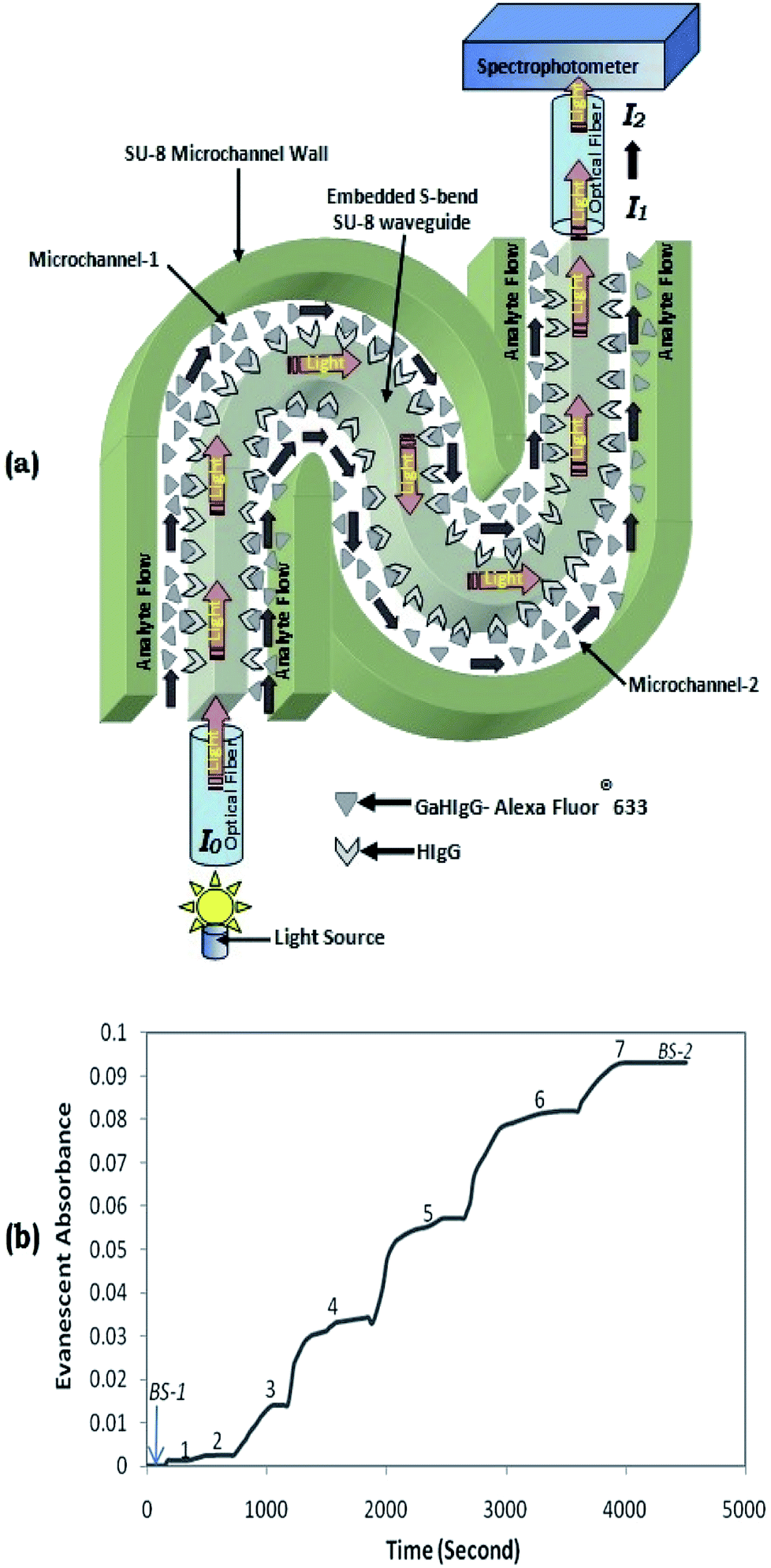 | ||
| Fig. 12 (a) Schematic diagram of light-ray propagating in an embedded S-bend waveguide-based biosensing probe. (b) Real-time shift in absorbance (at λ = 630 nm) observed from a HIgG-immobilized S-bend waveguide-based biosensing probe after they were introduced to (1) 0.1 μg mL−1 (2) 0.25 μg mL−1, (3) 0.5 μg mL−1; (4) 1 μg mL−1, (5) 2.5 μg mL−1, (6) 5 μg mL−1, and (7) 10 μg mL−1, Alexa Fluor®633-tagged GaHIgG solutions in the coupled microchannel system of the device until we attained the saturation. Here, BS-1 & BS-2 indicate introduction of the buffer solution (without any labeled GaHigG concentration), initially, during the experiments, and finally, after the completion of experiments, respectively. | ||
Fig. 12a represent the schematic diagram of light-ray propagating in a biosensing probe based on a dual microchannel embedded S-bend waveguide. It presents how a S-shaped waveguide-based biosensing probe coupled to a light source (intensity = I0) via an optical fiber shows a change in light output intensity from I1 to I2 as the antigen (i.e., Alexa Fluor®633-tagged GaHIgG) is attached to the bioreceptor HIgG. Fig. 12(b) corresponds to a real-time shift in absorbance recorded from a HIgG-immobilized S-bend waveguide probe while they were introduced to (1) 0.1 μg mL−1 (2) 0.25 μg mL−1, (3) 0.5 μg mL−1; (4) 1 μg mL−1, (5) 2.5 μg mL−1, (6) 5 μg mL−1, and (7) 10 μg mL−1, Alexa Fluor®633-tagged GaHIgG, antigen solutions. Here, BS-1 represents the absorbance trends during the initial introduction of buffer solution in the coupled microchannels, before the injection of the aforementioned antigen concentration.
Contrary to our earlier reported studies,12,13,15,16 to separate each of the successively introduced elevated concentration labeled GaHIgG solution from the lesser one, the sample microreservoir was usually not purged with air or nitrogen, after each lower concentration labeled GaHIgG solution injection. This is due to a higher possibility of air bubble entrapment in the relatively complex microchannel network (coupled to an S-bend waveguide) during the air purging, which usually leads to an unpredictable change in absorbance and may cause interference with the actual results.
Finally, to remove residual antigens in the microchannel embedding S-bend waveguide, which remain unbound to the antibodies, namely HIgG (immobilized over the dual-bend waveguide surfaces), was flushed with buffer solutions for a few minutes (BS-2, of Fig. 12b); further, the final change in absorbance was measured. Owing to the binding of Alexa Fluor®633-tagged GaHIgG to the waveguide surface immobilized HIgG, the saturated absorbance response was found to be 0.094. To test the capability of the biosensor probes for real-time continuous monitoring, the absorbance response was observed for ∼1 h. Consequently, this lab on a chip device was competent for detecting a concentration of ∼0.11 μg mL−1 of the GaHIgG analyte.
6. Concluding remarks
A novel single-step fabrication procedure (using SU8 photoresist), was performed to produce these devices, which consisted of waveguides structure (having a different orientation of two C-bends, i.e., S-bend and spiral-bend), embedded & interfaced (at their inner and outer bend surfaces) with a defined shape microchannel system along with fiber-to-waveguide coupler structures.The evanescent sensing efficiency of the two embedded dual-bend polymer waveguides designs was analyzed and demonstrated by suitable calculations and experiments. Calculations revealed a ∼22% higher sensitivity in the case of the embedded S-shaped waveguides, compared to spiral waveguides of the same length. The evanescent wave absorption by fluids present in the microchannels/microreservoir was confirmed by absorption measurements with various concentrations of methylene blue solutions. The limit of detection was found to be a minimum of 1 μM in the case of embedded S-bend/spiral waveguides which is lower than 10 μM for embedded (outer bend surface) U-bend waveguides.12,13 Experimentally, S-bend waveguides were found to be ∼25% higher in sensitivity compared to that of similar dimension spiral waveguides. Compared to embedded U-bend waveguides, the overall evanescent-wave-absorption-based detection sensitivity of embedded spiral and S-shaped waveguides were improved by ∼7 times and ∼9 times, respectively. These embedded waveguides probes were proved to be a suitable device for analyzing optically absorbing analyte molecules. Finally, an appropriate high optical power light sources (in 600–650 nm wavelength ranges), as well as bioreceptor: human IgG (HIgG), and analyte: Alexa Fluor®633-labeled GaHIgG biomolecules (λmax = 632 nm) were selected to prove the efficiency of this device for biosensing applications. These devices were shown to be capable of detecting a concentration of ∼0.11 μg mL−1 of these labeled GaHIgG analytes.
The aforesaid problems (that appeared in earlier devices), concerning fixed analyte volume interaction and sample evaporation;16 which may lead to variable absorbance output for introduced similar analyte concentrations, were resolved in the present devices. Further, a smooth handling of different analyte sample concentrations, in terms of, their easy sequential introduction in to microchannel (coupled to given waveguide), also gives this device a positive advantage in terms of enabling the easy continuous analysis of different concentrations of analyte solutions. Furthermore, the real-time analysis of any biological/chemical interaction between any two (bio)molecules (which leads to a change in the optical property of solution) is possible with this device, by simply circulating the analyte solutions through the microchannel system of the presented device and by measuring the respective real-time evanescent-absorbance values.
Considering the optical transmission property, other materials, i.e., glass, quartz, silicon oxide, silicon nitride, PDMS, PMMA, etc., are clearly superior for device fabrication compared to SU8; however, the fabrication process, together with these materials, will be much more difficult and costlier. Despite the internal complex structure of the presented device, its inlet can be easily coupled to other components of a complete lab on chip analytical system. Research work is progressing to connect this device to earlier reported microfluidic blood plasma separation devices23–25 for a cost effective, throwaway, sensitive Lab on chip system for plasma analyte (bio)sensing. Ultimately, the device can be comprehended to be a valuable and versatile sensing platform for any physical (refractive index deviation based), chemical (evanescent-field-absorption based), and biological (evanescent-field-absorption based) sensing applications, if suitable surface adaptation is performed to the embedded S-bend waveguide probe.
Conflicts of interest
There are no conflicts to declare.Acknowledgements
Authors are sincerely thankful to Dr Sunny Sharma, IIIT Allahabad for his help and support. The authors are also thankful to CEN (Centre of Excellence in Nanotechnology), IIT Bombay and VLSI lab, IIIT Allahabad for providing waveguide fabrication facilities. Financial support from the Department of Science and Technology (DST) with grant number: DST/TM/WTI/2K15/201, and Science & Engineering Board (SERB) with grant number: SR/FTP/ETA-0126/2014 is also acknowledged, for developing a reasonable micro-fabrication and device characterization facilities at “Bio-MEMs and Nanotechnology Lab”, IIIT Allahabad, in this respect. Support from Wadhwani Research Center for Bioengineering (WRCB), IIT Bombay is also acknowledged.References
- M. D. De Grandpre and L. W. Burgess, Appl. Spectrosc., 1990, 44, 273 CrossRef CAS.
- T. B. Colin, K. H. Yang and W. C. Stwalley, Appl. Spectrosc., 1991, 45, 1291 CrossRef CAS.
- V. Ruddy, Opt. Eng., 1994, 33, 3891 CrossRef CAS.
- B. D. Gupta and C. D. Singh, Appl. Opt., 1994, 33, 2737 CrossRef CAS PubMed.
- D. Littlejohn, D. Lucas and L. Han, Appl. Spectrosc., 1999, 53(7), 845–849 CrossRef CAS.
- S. K. Khijwania and B. D. Gupta, Opt. Quantum Electron., 1999, 31(8), 625–636 CrossRef CAS.
- G. Mignani, R. Falciai and L. Ciaccheri, Appl. Spectrosc., 1998, 52(4), 546–551 CrossRef.
- V. Joel, D. Luna-Moreno and D. Monzón-Hernández, Sens. Actuators, B, 2005, 110, 23–27 CrossRef.
- M. Ahmad and L. L. Hench, Biosens. Bioelectron., 2005, 20(7), 1312–1319 CrossRef CAS PubMed.
- P. N. Moar, S. T. Huntington, J. Katsifolis, L. W. Cahill, A. Roberts and K. A. Nugent, J. Appl. Phys., 1999, 85(7), 3395–3398 CrossRef CAS.
- B. D. Gupta, H. Dodeja and A. K. Tomar, Opt. Quantum Electron., 1996, 28, 1629–1639 CrossRef CAS.
- A. Prabhakar and S. Mukherji, Lab Chip, 2010, 10, 748–754 RSC.
- A. Prabhakar and S. Mukherji, Lab Chip, 2010, 10, 3422–3425 RSC.
- N. Punjabi, A. Khatri and S. Mukherji, Proc. SPIE 8924, Fourth Asia Pacific Optical Sensors Conference, 89241W, October 15, 2013, DOI:10.1117/12.2031384.
- A. Prabhakar and S. Mukherji, Sens. Actuators, B, 2012, 171–172, 1303–1311 CrossRef CAS.
- A. Prabhakar, N. Mishra and S. Mukherji, J. Microelectromech. Syst., 2017, 26(4), 935–945 CAS.
- R. Siebert and J. Muller, Sens. Actuators, A, 2005, 119, 138–149 CrossRef CAS.
- Z. Han, P. Lin, V. Singh, L. Kimerling, J. Hu, K. Richardson, A. Agarwal and D. T. H. Tan, Appl. Phys. Lett., 2016, 108, 141106 CrossRef.
- V. M. Lavchiev, B. Jakoby, U. Hedenig, T. Grille, P. Irsigler, G. Ritchie, J. Kirkbride and B. Lendl, Sensors, IEEE, 2014, DOI:10.1109/ICSENS. 2014. 6985081.
- N. A. Feidenhans’l, J. P. Lafleur, T. G. Jensen and J. P. Kutter, Electrophoresis, 2014, 35, 282–288 CrossRef PubMed.
- W. Snyder and J. D. Love, Optical Waveguide Theory, Chapman & Hall, London, 1983, pp. 63–88 Search PubMed.
- A. Deepu, V. V. R. Sai and S. Mukherji, J. Mater. Sci.: Mater. Med., 2009, 20, S25–S28 CrossRef CAS PubMed.
- A. Prabhakar, Y. V. B. V. Kumar, S. Tripathi and A. Agrawal, Microfluid. Nanofluid., 2015, 18(5), 995–1006 CrossRef CAS.
- S. Tripathi, Y. V. B. V. Kumar, A. Prabhakar, S. Joshi and A. Agrawal, J. Micromech. Microeng., 2015, 25(8), 084004 CrossRef.
- S. Tripathi, Y. V. B. V. Kumar, A. Prabhakar, S. Joshi and A. Agrawal, J. Micromech. Microeng., 2015, 25(8), 083001 CrossRef.
Footnote |
| † Electronic supplementary information (ESI) available. See DOI: 10.1039/c8ra06527f |
| This journal is © The Royal Society of Chemistry 2018 |