
 Open Access Article
 This Open Access Article is licensed under a Creative Commons Attribution-Non Commercial 3.0 Unported Licence
Effect of metal doping on the visible light absorption, electronic structure and mechanical properties of non-toxic metal halide CsGeCl3
Md. Zahidur Rahaman and
A. K. M. Akther Hossain*
and
A. K. M. Akther Hossain*
Department of Physics, Bangladesh University of Engineering and Technology, Dhaka-1000, Bangladesh. E-mail: akmhossain@phy.buet.ac.bd; zahidur.physics@gmail.com
First published on 24th September 2018
Abstract
Non-toxic metal halide perovskites have become forefront for commercialization of the perovskite solar cells and optoelectronic devices. In the present study, for the first time we show that particular metal doping in CsGeCl3 halide can considerably enhance the absorbance both in the visible and ultraviolet light energy range. We have carried out DFT based first principles calculations on Mn-doped and Ni-doped CsGeCl3 halide. We investigate the detailed structural, optical, electronic and mechanical properties of all the doped compositions theoretically. The study of the optical properties shows that the absorption edge of both Ni and Mn-doped CsGeCl3 is shifted toward the low energy region (red shift) relative to the pristine one. An additional peak is observed for both doped profiles in the visible light energy region. The study of the mechanical properties demonstrates that both the doped samples are mechanically stable and ductile as the pristine CsGeCl3. The study of the electronic properties shows that the excitation of photoelectrons is easier due to the formation of intermediate states in Mn-doped CsGeCl3. As a result Mn-doped CsGeCl3 exhibits higher absorptivity in the visible region than the Ni-doped counterpart. A combinational analysis indicates that CsGe1−xMnxCl3 is the best lead free candidate among the inorganic perovskite materials for solar cell and optoelectronic applications.
1. Introduction
Inorganic metal halide perovskite materials have been a topic of great interest in recent years due to their unique properties and applications. Metal halides hold great promise as solar cell material and have also shown outstanding performance in optoelectronics. Inorganic metal halides possess remarkable optoelectronic properties including high optical absorption, small carrier effective mass, tunable band gap, point defect, high charge carrier mobility and long charge diffusion.1,2 The applications of these semiconductors are not limited to the branch of photovoltaics and optoelectronics; they have also a number of applications in photodetectors, LEDs (Light Emitting Diodes) and devices which are used for solar to fuel energy conversion.3–6 Moreover, these semiconducting materials are inexpensive and abundant on earth. Due to this reason, the use of these materials in solar cells is convenient and more economical than the Si-based photovoltaic technology (PV-Technology).1The well known formula of metal halide perovskites is ABX3 (where, A = a cation, B = a metal ion and X = a halogen anion). The majority of the materials which exhibit remarkable performances in this family contain lead (Pb). Therefore, the major concern for application of these materials in practice is the toxicity of Pb. In ambient conditions lead based metal halide perovskites decompose to PbI2 which is harmful to the environment.7–9 Hence, several theoretical and experimental studies have been carried out in recent years in the quest to find novel non-toxic perovskites by replacing lead with a non-toxic metal cation. Recently Roknuzzaman et al. carried out a detailed investigation on this group of materials by using theoretical methods to find a suitable lead free candidate.10 They performed a simulation study the structural, optical, electronic and mechanical properties of CsBX3 (B = Ge, Sn and X = Cl, Br, I) semiconductors and compare their results with the lead containing semiconductors CsPbX3 (X = Cl, Br, I). After a combinational analysis they suggest that Ge-based CsGeI3 metal halide is the best lead free inorganic metal halide perovskite semiconductor for optoelectronic and solar cell applications. However, the study of the mechanical properties shows that the proposed sample is brittle in nature and hence unsuitable for real world application.
In 2016, Erdinc et al. studied the electronic, optical, thermodynamic and lattice dynamical properties of CsGeCl3 semiconductor for both paraelectric and ferroelectric phases.11 Another experimental and theoretical study suggests that CsGeCl3 is a wide band gap semiconductor with an experimental band gap value of 3.67 eV.12–15 Because of this large band gap value CsGeCl3 metal halide is not perfect for solar cell application. However, an appropriate metal dopant in CsGeCl3 can reduce the band gap to such extent which is suitable for the absorption of visible light energy. Therefore, in the present study we aim to dope with different transition metals the Ge-site of the CsGeCl3 metal halide in order to extend its absorption spectra across all the range of the solar spectrum. We have studied the optical, electronic and mechanical properties of Ni and Mn-doped CsGeCl3 by using a Density Functional Theory (DFT) based theoretical method to find a better candidate in this family for solar cell and optoelectronic applications than the previously proposed best lead free candidate CsGeI3. Finally, a thorough comparison among the key properties of the metal doped CsGeCl3 and pristine CsGeCl3 with the CsGeI3 metal halide is presented and discussed in details.
2. Theoretical methodology
The theoretical calculations are performed by using the Density Functional Theory (DFT) based plane wave pseudopotential approach.16 All the calculations are implemented by using the Cambridge Serial Total Energy Package (CASTEP) executed within the Material Studio-7.0.17,25 In order to achieve the desired doping effect in pure cubic CsGeCl3 metal halide, a 2 × 2 × 2 supercell is constructed which contains 40 atoms. As a result, the new chemical formula of CsGeCl3 perovskite can be written as CsGe1−xMxCl3 (x = 0.125 and M = Ni, Mn). Generalized Gradient Approximation (GGA) proposed by Perdew, Burke and Ernzerhof (PBE) is used for evaluating the exchange correlation energy.18 The wave function is expanded up to 350 and 500 eV plane wave cutoff energy for doped and pristine samples, respectively. For ensuring the criteria of convergence for both the electronic properties calculation and geometry optimization 3 × 3 × 3 k-points and 10 × 10 × 10 k-points have been used for doped and pure sample, respectively. For describing the electron ion interaction Vanderbilt type ultrasoft pseudopotential is used.19 BFGS (Broyden–Fletcher–Goldfarb–Shanno) relaxation scheme is used for optimizing the crystal structure.20 The unit cell and atomic relaxations are performed as long as the residual forces are below 0.03 eV Å−1.Finite strain theory21 executed within the CASTEP module is used for evaluating the elastic constants of pristine and doped CsGeCl3 metal halide. We set 0.003 as the maximum strain amplitude. Voigt–Reuss–Hill (VRH) averaging scheme22 is used for obtaining the polycrystalline mechanical parameters from the evaluated Cij. The polycrystalline elastic moduli are calculated by using the equations given elsewhere.23 The optical properties are calculated by using the CASTEP tool based on the standard DFT Kohn–Sham orbitals.24 A scissor operator of 2.673 eV is applied in the calculation in order to compensate for the gap between the theoretical value (0.997 eV) and experimental value (3.67 eV) of the pure CsGeCl3 band gap.
3. Results and discussion
3.1. Structural properties
Inorganic metal halide perovskite semiconductor CsGeCl3 belongs to the space group Pm![[3 with combining macron]](https://www.rsc.org/images/entities/char_0033_0304.gif) m (221) with a cubic crystal structure.10 The unit cell consists of five atoms with only one formula unit. The fractional coordinates of the Cs, Ge and Cl atoms are (0, 0, 0), (0.5, 0.5, 0.5) and (0, 0.5, 0.5) with Wyckoff position 1a, 1b and 3c, respectively. The experimental lattice parameter and unit cell volume are listed in Table 1 with the theoretical values calculated in this study. For inserting impurities in CsGeCl3 perovskite a supercell having size 8 times the unit cell of the pristine sample is constructed as shown in Fig. 1. The supercell of CsGeCl3 contains 40 atoms including 8 Cs atoms, 8 Ge atoms and 24 Cl atoms. The impurities are inserted in pure CsGeCl3 by replacing one Ge atom by Ni/Mn atom (substitutional doping) which corresponds to the doping concentration of about 12.5 atom%. The evaluated unit cell parameters of pristine and doped samples are tabulated in Table 1.
m (221) with a cubic crystal structure.10 The unit cell consists of five atoms with only one formula unit. The fractional coordinates of the Cs, Ge and Cl atoms are (0, 0, 0), (0.5, 0.5, 0.5) and (0, 0.5, 0.5) with Wyckoff position 1a, 1b and 3c, respectively. The experimental lattice parameter and unit cell volume are listed in Table 1 with the theoretical values calculated in this study. For inserting impurities in CsGeCl3 perovskite a supercell having size 8 times the unit cell of the pristine sample is constructed as shown in Fig. 1. The supercell of CsGeCl3 contains 40 atoms including 8 Cs atoms, 8 Ge atoms and 24 Cl atoms. The impurities are inserted in pure CsGeCl3 by replacing one Ge atom by Ni/Mn atom (substitutional doping) which corresponds to the doping concentration of about 12.5 atom%. The evaluated unit cell parameters of pristine and doped samples are tabulated in Table 1.
 | ||
| Fig. 1 The crystal structure (2 × 2 × 2 supercell) of CsGeCl3 metal halide. (a) Three dimensional and (b) two dimensional view. | ||
3.2. Optical properties
In general, lead free (non-toxic) metal halide perovskites possess low reflectivity, high absorption coefficient and high optical conductivity compared to their lead containing counterpart. The study of optical properties is essential for discovering a suitable material in this family for the application in optoelectronic devices and solar cells. In this section of the paper the important optical parameters including absorption coefficient, reflectivity, real and imaginary part of dielectric constant and optical conductivity of pristine and Ni/Mn-doped CsGeCl3 are analyzed and discussed in details.The evaluated absorption profiles of pristine and doped CsGeCl3 are illustrated in Fig. 2. The optical absorption coefficient is defined as the fraction of energy (wavelength) absorbed per unit length of the material and provides crucial information about the efficiency of optimum solar energy conversion of a material. Fig. 2(a) exhibits the photon energy dependent absorption coefficient of both pure and doped CsGeCl3. According to the result, the absorption edge of both Ni and Mn-doped CsGeCl3 is shifted toward the low energy region (red shift) relative to the pristine one. An additional peak is observed for both doped profiles in the low energy region. The absorption edge of Mn-doped CsGeCl3 shifts more toward the lower energy region than Ni-doped CsGeCl3. The pristine CsGeCl3 shows no absorbance in the visible light region. The metal doping in pure CsGeCl3 enhances the absorption coefficient to a great extent not only in the visible region but also in the ultraviolet region. For a better understanding of the light absorption feature of CsGeCl3 in the visible region, the wavelength dependent absorption coefficient is presented in Fig. 2(b). As shown in Fig. 2(b) the Mn-doped CsGeCl3 has a wider absorption area than the Ni-doped CsGeCl3. The reason for the formation of the broadest absorption area in the Mn-doped sample will be discussed in details in the next section. In general, wide band gap semiconductors can absorb ultraviolet light of the solar spectrum which is only 4% of the total solar energy coming to the earth.26 The visible light covers approximately 43% of the solar spectrum.27 Therefore, the intrinsic CsGeCl3 (band gap = 3.67 eV) is incapable to utilize the visible light energy for photovoltaic conversion. Hence, the prominent absorption in the visible region in the Mn-doped sample shows great promise for better utilization of the solar spectrum and may increase the solar cell efficiency.
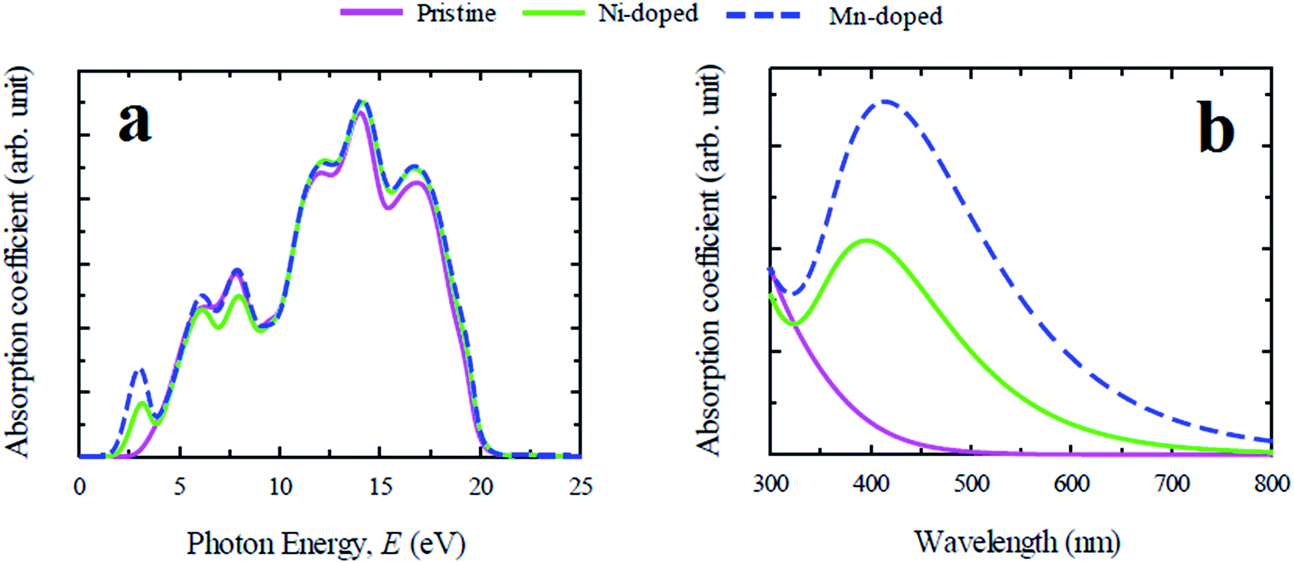 | ||
| Fig. 2 Calculated light absorption spectra of pure and metal doped CsGeCl3 perovskite. (a) Photon energy dependent and (b) wavelength dependent absorption coefficient. | ||
Reflectivity is one of the crucial optical properties of materials for photovoltaic applications and is defined as the amount of light energy reflected from the surface of a material with respect to the amount of light energy incident on the surface of the material. The reflectivity spectra of pristine and doped samples for photon energy up to 30 eV are illustrated in Fig. 3(a). CsGeCl3 shows low reflectivity in the whole energy range of the solar spectrum. However, the reflectivity of all metal doped samples is nearly identical to the pristine one in the ultraviolet region. An additional peak is observed in the visible region for all doped samples whereas Mn-doped CsGeCl3 has a stronger reflectivity in the low photon energy range than the Ni-doped sample. The dielectric function is characterized by the response of a material to the incident light energy. The charge carrier recombination rate and hence the overall performance of optoelectronic devices depends upon the static value of the dielectric function.28 A material with high dielectric constant has relatively less charge carrier recombination rate. As a result the overall performance of optoelectronic devices is enhanced. The real and imaginary part of the evaluated dielectric function of pure and doped CsGeCl3 are depicted in Fig. 3(c) and (d). It is evident that the Mn-doped sample shows relatively higher dielectric constant than the pure and Ni-doped CsGeCl3. Therefore, in terms of dielectric constant Mn-doped CsGeCl3 is a better candidate for solar cell and optoelectronic applications than the pristine one. Generally a material with a higher band gap exhibit lower dielectric constants.29 Since metal doping in CsGeCl3 decreases the band gap value (see Electronic properties section), the metal doped samples show a higher dielectric constant than the pure CsGeCl3. As shown in Fig. 3(c) and (d) overall the dielectric profile (both real and imaginary part) of the metal doped samples is almost identical in the high energy region (ultraviolet zone) to that of the pure sample. An additional peak of the real part of the dielectric constant is observed in the visible light energy zone. The imaginary part of the dielectric constant of all the samples goes to zero above 19 eV while the real part reaches approximately unity. This result implies that both doped and pure CsGeCl3 halide exhibit transparency with slight absorption in the high energy zone (above 19 eV) (it is also evident from the absorption coefficient graph [Fig. 2(a)]). The appearance of a sharp peak of the imaginary part of the dielectric constant of the metal doped sample in the visible region implies the occurrence of strong absorption in this region30 which also justifies the result obtained from the absorption spectra of doped CsGeCl3 [Fig. 2]. Therefore, the investigation of the dielectric constant of the pure and metal doped CsGeCl3 suggests that both pristine and doped sample possess high transmissivity in the high energy region (above 19 eV) and metal doped samples possess nearly zero transmissivity in the visible region. This is the reason for high absorptivity of metal doped CsGeCl3 (particularly Mn-doped CsGeCl3) in the visible region. However, the study of the reflectivity spectra [Fig. 3(a)] shows that Mn and Ni-doped CsGeCl3 have a slight higher reflectivity in the visible energy zone. Hence, further research should be conducted to reduce the reflectivity of the metal doped CsGeCl3 in the visible region which may further increase the absorptivity as well as efficiency of the solar cells. The optical conductivity is also defined as the photoconductivity. The conductivity spectra of doped and pristine CsGeCl3 are illustrated in Fig. 3(b) up to 25 eV light energy. The optical conductivity of the metal doped CsGeCl3 is almost similar to that of the pure sample in the high energy region. A sharp peak appeared in the visible light energy zone for both doped profiles whereas the Mn-doped sample exhibits a larger photoconductivity than the Ni-doped sample. The appearance of the large photoconductivity in the visible region for the metal doped CsGeCl3 is a consequence of its large absorptivity in the low energy region [Fig. 2].
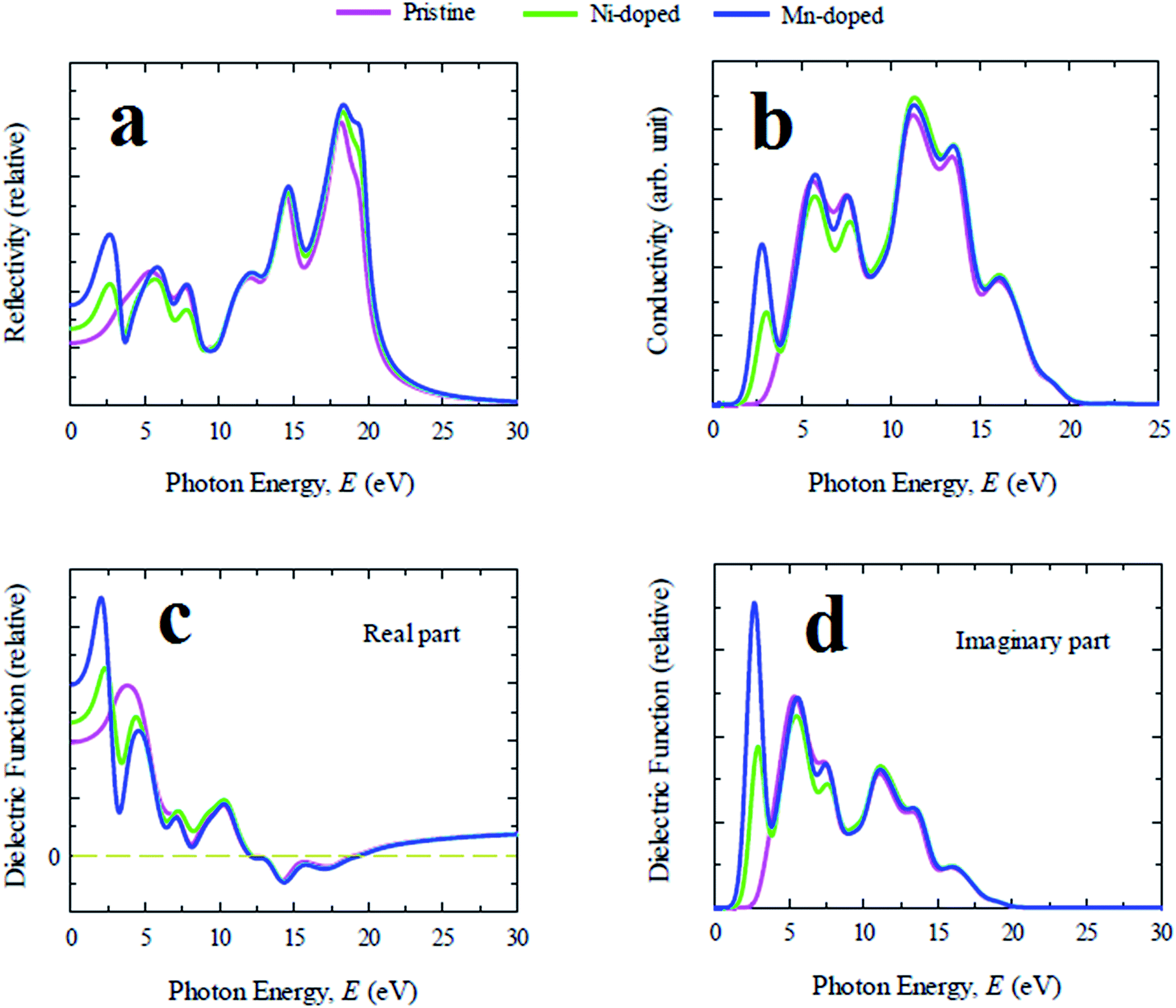 | ||
| Fig. 3 The simulated photon energy dependent (a) reflectivity, (b) conductivity, (c) real part of dielectric function and (d) imaginary part of dielectric function of pristine and transition metal doped CsGeCl3. | ||
3.3. Electronic properties
In order to explain the above optical features of the metal doped CsGeCl3 halide, the basic electronic properties including band structure and density of states (DOS) of the studied samples are calculated and discussed in this section. Fig. 4 illustrates the electronic band structures of pristine and metal doped CsGeCl3. The band structure diagram of the pure sample calculated using the single cell of CsGeCl3 is depicted in Fig. 4(a). As shown in the figure the conduction band minimum and valence band maximum lies at R (k-point), indicating the direct band gap (0.97 eV) nature of pristine CsGeCl3. This result is in accordance with the evaluated value of 0.978 eV by Roknuzzaman et al.10 implying the reliability of the present calculations. The band structure diagram illustrated in Fig. 4(b) is calculated by using the supercell (eight times) of CsGeCl3. The computed band gap (direct) of pristine CsGeCl3 is 0.997 eV showing a good agreement with the band gap value calculated using the single cell of CsGeCl3. It is evident that the computed band gap value underestimates the experimentally evaluated band gap value 3.67 eV.15 The reason for this can be attributed to the well known limitation of GGA. The Local Density Approximation (LDA) and LDA + U methods also underestimate the band gap value. Sometimes Heyd–Scuseria–Ernzerhof (HSE) hybrid potential may provide a band gap value close to the experimental one, but it is also not valid for all of the materials. Partial correction of the theoretical band gap value relative to the experimental one can be achieved by using the GGA + U approach. However, we only focus on the variation of the band gap due to different metal doping in CsGeCl3 and ignore the band gap error of the GGA approach. The band structure profile of metal doped CsGeCl3 halide is illustrated in Fig. 4(c) and (d), respectively. It is evident that impurity states emerge within the band gap of Ni-doped sample, whereas intermediate states appear within the band gap of Mn-doped CsGeCl3. In case of the Ni-doped sample [Fig. 4(c)], vacant states are formed over the Fermi level. The valence band is extended into the higher energy region. The extension of the valence band into the Fermi level can facilitate the transition of electrons from the valence band to the conduction band. However, the gap between the maximum of the valence band and the minimum of the conduction band is 1.10 eV which is larger than the band gap value of pristine CsGeCl3 (0.997 eV). The enhancement of the band gap shows a contradiction with the optical absorbance of Ni-doped CsGeCl3. Here, the shift of the Fermi level into the valence band can be defined as the negative Burstein shift. This broadening of the band gap can be ascribed to the phenomena known as Moss–Burstein effect.31 Therefore, ignoring the Moss–Burstein shift the band gap of the Ni-doped sample is reduced and causes the occurrence of absorbance in the visible region [Fig. 2(b)]. As shown in Fig. 4(d) in case of the Mn-doped CsGeCl3 halide, an intermediate energy band appeared in the band gap. The energy gap between the valence band and the conduction band is 0.97 eV (similar to the pristine one) but the energy gap between the minimum of the conduction band and the top of the intermediate states is 0.29 eV which is much smaller than the band gap value of pure CsGeCl3. Thus, the excitation of photo electrons is easier due to the formation of these intermediate states in the Mn-doped CsGeCl3. As a result Mn-doped CsGeCl3 exhibits a higher absorptivity in the visible region than the Ni-doped counterpart. It should also be noted that the band gap of the Mn-doped sample [Fig. 4(d)] is indirect and hence photons with this band gap energy can generate electron–hole pairs with the aid of phonons similar to silicon.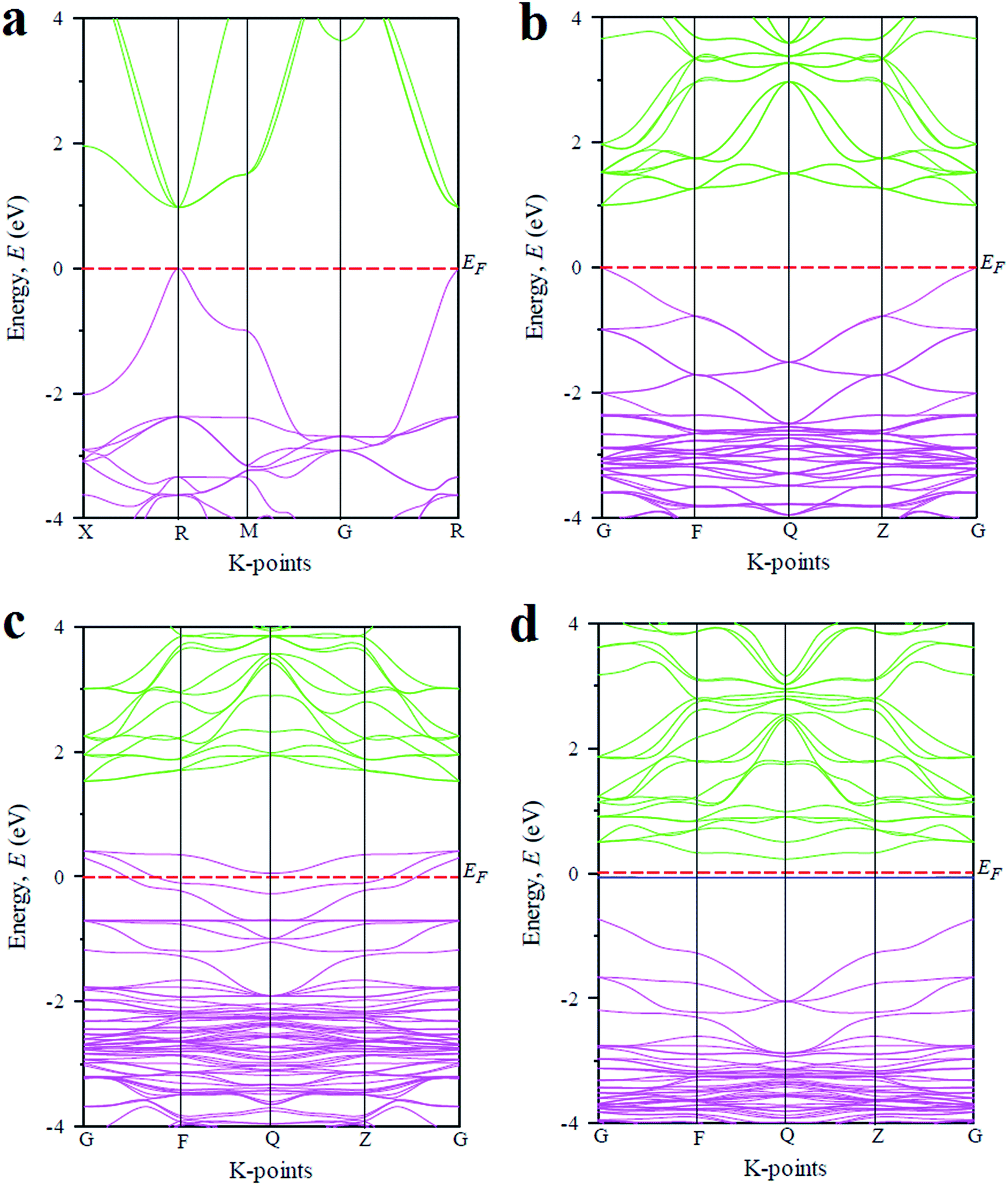 | ||
| Fig. 4 The band structure diagram of CsGeCl3 metal halide calculated by using (a) pure single cell, (b) pure supercell, (c) Ni-doped and (d) Mn-doped sample. | ||
The total and partial density of states of pristine and doped CsGeCl3 are depicted in Fig. 5. Fig. 5(a) illustrates the DOS profile of the pure sample. As shown in the figure the valence band is mostly composed of Cl-3p and Ge-4p orbitals with a small contribution of Cs-6s and Cs-5p orbitals. The conduction band mainly consists of Ge-4p orbital with a small contribution of Cs-6s and Cs-5p orbitals. After Ni doping in CsGeCl3 a slight change is observed in the overall DOS profile as shown in Fig. 5(b). The composition of the valence band is almost similar to that of the pristine sample except for an extra peak which appeared in the total DOS due to the formation of dopant states (Ni-3d) in the valence band of CsGeCl3. The composition of the conduction band is similar to the pristine one as no dopant peak is formed. A similar trend is observed for the Mn-doped sample as shown in Fig. 5(c). The conduction band slightly shifts toward the lower energy region. A flat peak is observed in the conduction band due to the formation of dopant states (Mn-3d) in the conduction band. Fig. 5(d) illustrates the change of the band gap due to the formation of new dopant states near the Fermi level. In case of Ni-doped CsGeCl3 the impurity energy states are formed over the Fermi level and mixed with the valence band maximum. These impurity states can trap the photoexcited holes which reduce the recombination rate of electrons and holes.32 In case of Mn-doped CsGeCl3 the impurity energy states appear in the middle of the band gap. These intermediate states reduce the energy which is necessary for electron transition to occur from the valence band to the conduction band. The valence electrons are first excited to the impurity energy states (intermediate band) and then excited to the conduction band by consuming the visible light energy. These results explain the red shift of the absorption spectra as shown in Fig. 2.
 | ||
| Fig. 5 The total and partial density of states of CsGeCl3 metal halide simulated by using (a) pure supercell, (b) Ni-doped sample, (c) Mn-doped sample and (d) dopant contribution at the Fermi level. | ||
3.4. Mechanical properties
For ensuring the mechanical stability of the metal doped CsGeCl3 halide the elastic constants of the doped phases are calculated and discussed in this section in details. The calculated elastic constants of pristine and doped CsGeCl3 are tabulated in Table 2. It is evident that all the compositions fulfill the well established Born stability criteria33 given as follows,| C11 > 0, C44 > 0, C11 − C12 > 0 and C11 + 2C12 > 0 |
| Phase | C11 | C12 | C44 | C12–C44 |
|---|---|---|---|---|
| CsGeCl3 | 55.02 | 13.14 | 11.73 | 1.41 |
| CsGe1−xNixCl3 | 54.16 | 14.60 | 13.36 | 1.24 |
| CsGe1−xMnxCl3 | 56.68 | 14.36 | 13.33 | 1.03 |
| CsGeCl3 (ref. 10) | 54.93 | 13.08 | 11.99 | — |
Hence, both the doped phases are mechanically stable in nature. It is also evident that the calculated elastic constants of pristine CsGeCl3 (by using supercell) agrees well with the available theoretical result bearing the reliability of the present investigation. The Cauchy pressure (C12–C44) is a useful parameter to predict the brittleness and ductility of materials. The negative (positive) value of this parameter indicates the brittle (ductile) nature of a compound.30 The computed values of the Cauchy pressure of pristine and doped samples are positive [Table 2] implying that the doped samples are ductile as the pristine CsGeCl3.10
By using the computed elastic constants the most important mechanical parameters of a compound such as the shear modulus G, bulk modulus B, Young’s modulus E, B/G ratio and Poisson’s ratio ν of pristine and doped samples are calculated and listed in Table 3. It is also evident from Table 3 that all the calculated mechanical parameters show good consistency with the theoretically calculated results. The bulk modulus is one of the essential mechanical parameter which gives an indication of the stiffness of a material. The calculated bulk modulus of all the composition is comparatively low indicating the flexibility of all the samples. The value of B is slightly increased after Ni and Mn doping. However, this lower value of B ensures that it will be easier to make thin films of Mn-doped CsGeCl3 perovskite and hence suitable for solar cell applications. The shear modulus is used to calculate the plastic deformation of a material under external stress. As shown in Table 3 the value of G for all the samples is comparatively low. The value of G is slightly increased after Ni and Mn doping into CsGeCl3. However, the lower value of the shear modulus implies that CsGe1−xMnxCl3 is less rigid than the pristine sample and hence can be drawn into a desired shape. A similar trend is noticed for the Young’s modulus of all the compositions.
| Phase | B (GPa) | G (GPa) | E (GPa) | ν | B/G |
|---|---|---|---|---|---|
| CsGeCl3 | 27.11 | 14.82 | 37.60 | 0.26 | 1.82 |
| CsGe1−xNixCl3 | 27.78 | 15.63 | 39.48 | 0.26 | 1.77 |
| CsGe1−xMnxCl3 | 28.46 | 16.05 | 40.53 | 0.26 | 1.77 |
| CsGeCl3 (ref. 10) | 27.03 | 15.02 | 38.02 | 0.27 | 1.80 |
The Poisson’s ratio is another useful parameter for explaining the bonding nature and plasticity of a material. The calculated value of ν for all the compositions is 0.26 implying the existence of a central force in all the samples.34 However, all the samples should have predominant ionic feature as the value of ν is very close to the critical value of 0.25 which indicates an ionic crystal. The Poisson’s ratio is another useful indicator of ductility and brittleness of materials. The critical value for separating the ductility and brittleness of a material is 0.26.35 Surprisingly the computed value of ν of all the samples is exactly 0.26 thus implying the ductile nature of all the compositions. The ratio between bulk modulus and shear modulus is usually known as Pugh’s ratio which is also used to predict the failure mode of a material. In this case, the critical value for separating the ductility and brittleness of a material is 1.75.36 As shown in Table 3 all the studied compositions are ductile in nature as the value of B/G is greater than the critical value. The value of B/G is decreased after Ni and Mn doping in CsGeCl3. However, the value of Pugh’s ratio of metal doped CsGeCl3 perovskite is still greater than the critical value and hence should exhibited a ductile response as the pristine sample.
3.5. Environmentally-friendly perovskites
Among the lead free inorganic perovskite materials suitable for solar cell and optoelectronic applications CsGeI3 perovskite compound is proposed to be the best candidate.10 Though the band gap of CsGeI3 is suitable for the absorption of both visible and ultraviolet light energy of the solar spectrum, it is slightly brittle. Hence fabrication of solar cells using CsGeI3 halide is difficult. On the other hand, CsGeCl3 is ductile but possesses a large band gap which is not suitable for the absorption of visible light energy of the solar spectrum. Metal doping in CsGeCl3 can solve this problem.According to the present study, a small amount of Ni dopant in the Ge site of CsGeCl3 can elevate the absorption in the visible region to a great extent. However, the Mn-doped CsGeCl3 exhibits a very high absorption not only in the visible region but also in the ultraviolet region. The study of the mechanical properties shows that the proposed sample is ductile and possesses a low bulk modulus and hence it is possible to use it to make thin films. It also possesses high photoconductivity. The comparison among the key properties of pure and metal doped CsGeCl3 with CsGeI3 is presented in Table 4. From Table 4 it is clear that CsGe1−xMnxCl3 is the best lead free candidate among the inorganic perovskite materials for solar cell and optoelectronic applications.
| Properties | CsGeCl3,10 [this work] | CsGeI3 (ref. 10) | CsGe1−xNixCl3 | CsGe1−xMnxCl3 |
|---|---|---|---|---|
| Optical absorption | High in UV-region | High in UV-region | High in UV-region | High in UV-region |
| Missing in visible region | Medium in visible region | Medium in visible region | High in visible region | |
| Photoconductivity | Medium | High | Medium | High |
| Failure mode | Ductile | Brittle | Ductile | Ductile |
| Suitability for solar cells | Not good | Good | Better | Best |
4. Conclusions
In summary, by using the density functional theory dependent ab initio method the optical, electronic and mechanical properties of metal doped CsGeCl3 halide are investigated and discussed in details. The intrinsic CsGeCl3 is incapable to utilize the visible light energy for photovoltaic conversion due to its large band gap energy 3.67 eV. The selection of suitable metal dopants in CsGeCl3 halide can considerably enhance the absorbance and photoconductivity both in the visible and ultraviolet light energy range. However, due to the formation of an intermediate energy band the Mn-doped CsGeCl3 exhibits a higher absorptivity and photoconductivity in the visible region than the Ni-doped counterpart. Hence, the prominent absorption in the visible region of Mn-doped sample shows great promise for better utilization of the solar spectrum and may increase the solar cell efficiency. The study of mechanical properties shows that the Mn-doped CsGeCl3 is ductile and possesses a low bulk modulus. Therefore, it is also possible to make thin films by using CsGe1−xMnxCl3. The comparison among the key properties of pure and metal doped CsGeCl3 with the best known inorganic metal halide perovskite CsGeI3 suggests that CsGe1−xMnxCl3 is the best lead free candidate among inorganic perovskite materials for solar cell and optoelectronic applications.Conflicts of interest
There are no conflicts to declare.Acknowledgements
This work was carried out in the Solid State Physics Research Laboratory, Department of Physics, Bangladesh University of Engineering and Technology, Dhaka, Bangladesh.References
- W. Zhang, G. E. Eperon and H. J. Snaith, Metal halide perovskites for energy applications, Nat. Energy, 2016, 1(6), 16048 CrossRef.
- W.-J. Yin, T. Shi and Y. Yan, Unique properties of halide perovskites as possible origins of the superior solar cell performance, Adv. Mater., 2014, 26(27), 4653–4658 CrossRef PubMed.
- Q. A. Akkerman, et al., Strongly emissive perovskite nanocrystal inks for high-voltage solar cells, Nat. Energy, 2017, 2(2), 16194 CrossRef.
- G. E. Eperon, et al., Inorganic caesium lead iodide perovskite solar cells, J. Mater. Chem. A, 2015, 3(39), 19688–19695 RSC.
- T. Krishnamoorthy, et al., Lead-free germanium iodide perovskite materials for photovoltaic applications, J. Mater. Chem. A, 2015, 3(47), 23829–23832 RSC.
- P. Ramasamy, et al., All-inorganic cesium lead halide perovskite nanocrystals for photodetector applications, Chem. Commun., 2016, 52(10), 2067–2070 RSC.
- A. Babayigit, et al., Assessing the toxicity of Pb-and Sn-based perovskite solar cells in model organism Danio rerio, Sci. Rep., 2016, 6, 18721 CrossRef PubMed.
- G. E. Eperon, et al., The importance of moisture in hybrid lead halide perovskite thin film fabrication, ACS Nano, 2015, 9(9), 9380–9393 CrossRef PubMed.
- A. Babayigit, et al., Toxicity of organometal halide perovskite solar cells, Nat. Mater., 2016, 15(3), 247 CrossRef PubMed.
- M. Roknuzzaman, et al., Towards lead-free perovskite photovoltaics and optoelectronics by ab initio simulations, Sci. Rep., 2017, 7(1), 14025 CrossRef PubMed.
- B. Erdinc, et al., Ab initio study of CsGeCl3 compound in paraelectric and ferroelectric phases, Ferroelectrics, 2016, 494(1), 138–149 Search PubMed.
- D.-K. Seo, et al., Pressure-induced changes in the structure and band gap of CsGeX3 (X= Cl, Br) studied by electronic band structure calculations, Inorg. Chem., 1998, 37(3), 407–410 CrossRef PubMed.
- D. Huang, et al., First-principles prediction of a promising p-type transparent conductive material CsGeCl3, Appl. Phys. Express, 2014, 7(4), 041201 CrossRef.
- B. Erdinc, et al., Ab initio study of CsGeCl3 compound in paraelectric and ferroelectric phases, Ferroelectrics, 2016, 494(1), 138–149 Search PubMed.
- L.-C. Tang, et al., First principles calculations of linear and second-order optical responses in rhombohedrally distorted perovskite ternary halides, CsGeX3 (X= Cl, Br, and I), Jpn. J. Appl. Phys., 2009, 48(11R), 112402 CrossRef.
- M. C. Payne, et al., Iterative minimization techniques for ab initio total-energy calculations: molecular dynamics and conjugate gradients, Rev. Mod. Phys., 1992, 64(4), 1045 CrossRef.
- M. D. Segall, et al., First-principles simulation: ideas, illustrations and the CASTEP code, J. Phys.: Condens. Matter, 2002, 14(11), 2717 CrossRef.
- J. P. Perdew, K. Burke and M. Ernzerhof., Generalized gradient approximation made simple, Phys. Rev. Lett., 1996, 77(18), 3865 CrossRef PubMed.
- D. Vanderbilt, Soft self-consistent pseudopotentials in a generalized eigenvalue formalism, Phys. Rev. B: Condens. Matter Mater. Phys., 1990, 41(11), 7892 CrossRef.
- T. H. Fischer and A. Jan, General methods for geometry and wave function optimization, J. Phys. Chem., 1992, 96(24), 9768–9774 CrossRef.
- F. D. Murnaghan, Finite deformations of an elastic solid, Am. J. Math., 1937, 59(2), 235–260 CrossRef.
- R. Hill, The elastic behaviour of a crystalline aggregate, Proc. Phys. Soc., London, Sect. A, 1952, 65(5), 349 CrossRef.
- M. Z. Rahaman, M. A. Rahman and M. Abdur Razzaque Sarker, Prediction of a new transition metal oxide MgRhO3 with SrTiO3-type structure: Stability, structure and physical characteristics, Chin. J. Phys., 2017, 55(4), 1489–1494 CrossRef.
- CASTEP GUIDE MATERIALS STUDIO 8.0, 2014 Search PubMed.
- Materials Studio CASTEP Manual Accelrys, 2010, available at http://www.tcm.phy.cam.ac.uk/castep/documentation/WebHelp/CASTEP.html Search PubMed.
- W. Yu, J. Zhang and T. Peng, New insight into the enhanced photocatalytic activity of N-, C-and S-doped ZnO photocatalysts, Appl. Catal., B, 2016, 181, 220–227 CrossRef.
- X. Zong, et al., Activation of photocatalytic water oxidation on N-doped ZnO bundle-like nanoparticles under visible light, J. Phys. Chem. C, 2013, 117(10), 4937–4942 CrossRef.
- X. Liu, et al., A high dielectric constant non-fullerene acceptor for efficient bulk-heterojunction organic solar cells, J. Mater. Chem. A, 2018, 6(2), 395–403 RSC.
- M. Roknuzzaman, et al., Insightinto lead-free organic–inorganic hybrid perovskites for photovoltaics and optoelectronics: A first-principles study, Org. Electron., 2018, 59, 99–106 CrossRef.
- M. Z. Rahaman and M. A. Rahman, Investigation of the physical properties of two Laves phase compounds HRh2 (H = Ca and La): A DFT study, Int. J. Mod. Phys. B, 2018, 32(12), 1850149 CrossRef.
- E. Burstein, Anomalous optical absorption limit in InSb, Phys. Rev., 1954, 93(3), 632 CrossRef.
- Z. Zhao and Q. Liu, Effects of lanthanide doping on electronic structures and optical properties of anatase TiO2 from density functional theory calculations, J. Phys. D: Appl. Phys., 2008, 41(8), 085417 CrossRef.
- M. Born, On the stability of crystal lattices. I., Mathematical Proceedings of the Cambridge Philosophical Society, Cambridge University Press, 1940, vol. 36, iss. 2 Search PubMed.
- B. G. Pfrommer, et al., Relaxation of crystals with the quasi-Newton method, J. Comput. Phys., 1997, 131(1), 233–240 CrossRef.
- M. Z. Rahaman, M. L. Ali and M. A. Rahman, Pressure-dependent mechanical and thermodynamic properties of newly discovered cubic Na2He, Chin. J. Phys., 2018, 56(1), 231–237 CrossRef.
- S. F. Pugh, XCII. Relations between the elastic moduli and the plastic properties of polycrystalline pure metals, London, Edinburgh Dublin Philos. Mag. J. Sci., 1954, 45(367), 823–843 CrossRef.
| This journal is © The Royal Society of Chemistry 2018 |