DOI:
10.1039/C8RA06283H
(Paper)
RSC Adv., 2018,
8, 31608-31617
Using special Janus nanobelt as constitutional unit to construct anisotropic conductive array membrane for concurrently affording color-tunable luminescence and superparamagnetism†
Received
25th July 2018
, Accepted 28th August 2018
First published on 10th September 2018
Abstract
We have used electrospinning technology to fabricate a tri-functional nanobelt array membrane exhibiting tunable anisotropic electrical conduction, superparamagnetism and color-tunable luminescence by using a lab-made co-axis//single-axis spinneret and an aluminum drum collection device. Each one-dimensional (1D) Janus nanobelt is composed of luminescent-superparamagnetic bifunctional [Fe3O4/polymethyl methacrylate (PMMA)]@[Tb(BA)3phen/Eu(BA)3phen/PMMA] coaxial nanobelt and conducting polyaniline (PANI)/PMMA nanobelt. Moreover, all Janus nanobelts are aligned in the same manner to generate a two-dimensional (2D) array film. The conductance along the length is much stronger than the conductance in the width (two perpendicular directions). Therefore, the array membrane has excellent anisotropic electrical conduction. The conduction ratio reaches 108 times between the length and width of the Janus nanobelt array membrane, which is the highest conduction ratio between the two perpendicular directions for nanobelt materials reported internationally. Furthermore, we can modulate the degree of electrically conducting anisotropy of the samples by varying the amount of PANI. In addition, the Janus nanobelt array membrane is concurrently endowed by superior and adjustable superparamagnetism and photoluminescence. Importantly, the innovative philosophy and manufacturing technique of the new Janus nanobelt array membrane provide an easy way to prepare multifunctional nano-membranes.
Introduction
Anisotropic conducting film (ACF) is a new type of electronic composite material, which exhibits one direction conduction and other direction insulation. ACFs are widely used in micro-electronic packages, electrode conjuncture and other fields. ACFs can be divided into type I and type II ACFs in accordance with their conducting properties. In terms of type I ACFs, the directions along the film thickness and surface are conducting and insulating, respectively. The preparation technology of type I ACFs is advanced and widely used in the manufacture of modern electronic devices. Type II ACFs are single-layer or multi-layer thin films composed of parallel 1D conducting cells with different conductivities and different directions on the surface. These 1D conductors are mainly ultrafine fibers or long chains of molecules that guide electricity, which are separated by weak conductors such as air and/or interfaces. According to this particular structure, electrons move along the length of a 1D conducting element, but they are blocked vertically by air or an interface. Therefore, high conductivity can be observed along the length of the conducting element; however, low conductivity can be observed perpendicular to the length. Kovtyukhova et al.1 fabricated multiple layers of SWNTox/polymer membranes by conventional layer and layer assembly; the vertical conductance was 103 times lower than that along the length. Liu et al.2 prepared anisotropic conducting polymer films by electrospinning. The conductivity of the film along the vertical dimension was 106 times lower than that along the length. Huang et al.3 fabricated an anisotropic conducting polymer membrane. The results showed that the resistivity along the stripe was 6 orders of magnitudes higher compared with the resistivity along the orthogonal MWCNT stripe. At present, many serious weaknesses of the type II ACFs remain; thus, type II ACFs cannot be used in industry and can only be studied in the laboratory. Much research needs to be done on type II ACFs before their large-scale industrialization or applications. Therefore, solving or alleviating these defects is an urgent research topic.
There are three ways to fabricate anisotropic conducting polymer nanomaterials. The first way is to orient the conducting material into the polymer and endow the polymer film with conducting anisotropy characteristics.4 The second way is to apply an anisotropic conducting belt as a synthetic unit;5,6 for example, Ma et al. used the electrospinning technique to prepare an array film made of conducting anisotropic Janus nanobelts and microbelts. Because of this unique structure, the conductivities along the perpendicular and length dimensions of the belts are up to 108 times in disparity. The third way is to assemble the layered synthetic material into a strip 1D chain in a polymer. On this basis, several kinds of polymers in the strip chain and one dimensional chain technology, including shear assembly within magnetic field-induced self-assembly, guided by template assembly and nano filler and block copolymer collaborative assembly can be developed.
Electrospinning is the most convenient method to convert a viscous solution into a successive fiber with diameter ranging from micron to nanometer under high voltage.7–9 This technology has been popularized in the sectors of regenerative biology, electrochemical materials, optical fiber humidity sensors and filtration materials. At present, multifunctional nanomaterials are one of the hot topics in research.10 For photoelectromagnetic nanomaterials, a previous study by our research team and other researchers demonstrated that dark colored magnetic Fe3O4 nanoparticles (NPs) and conducting PANI greatly decrease the photoluminescence properties of rare earth (RE) compounds as they are blended.11 Up to now, our scientific team has fabricated some multifunctional nanomaterials through electrospinning technology, which contain coaxial nanocables,12 coaxial nanobelts,13 Janus nanoribbons,14 and Janus nanofibers.15,16 The 1D structures mentioned above can offer two independent partitions: RE compounds in one partition and Fe3O4 NPs and PANI in other partition. This special nanostructure can effectively separate RE compounds from Fe3O4 NPs and PANI, resulting in significant reduction in the luminescence of RE compounds by Fe3O4 NPs and PANI. The experiment also showed that while Fe3O4 NPs and PANI are mixed in one partition, Fe3O4 NPs cause PANI to be discontinuous in the nanofiber/nanobelt, thereby reducing the electrical conductivity of the nanomaterials. It is therefore necessary to further isolate the luminescent, magnetic and electrically conducting materials if the powerful photoluminescence performance and high conductance of the multifunctional nanomaterials are to be attained. To achieve this innovative academic concept, in this study, we developed a {[Fe3O4/PMMA]@[Tb(BA)3phen/Eu(BA)3phen/PMMA]}//[PANI/PMMA] (defined as [Magnetic@Luminescent]//Electrical, abbreviated as [M@Lum]//E) Janus nanobelt to implement three separate functional partitions included in one Janus nanobelt. The [M@Lum]//E Janus nanobelt was composed of two distinct sides comprising a [Fe3O4/PMMA]@[Tb(BA)3phen/Eu(BA)3phen/PMMA] coaxial nanobelt (magnetic-luminescent side) and a PANI/PMMA nanobelt (conducting side), and the Janus nanobelt successfully completed a variety of versatile asymmetric integrations. Furthermore, by using {[Fe3O4/PMMA]@[Tb(BA)3phen/Eu(BA)3phen/PMMA]}//[PANI/PMMA] as constitutional and conducting units, a {[Fe3O4/PMMA]@[Tb(BA)3phen/Eu(BA)3phen/PMMA]}//[PANI/PMMA] Janus nanobelt array membrane (abbreviated as [M@Lum]//E JAM) was obtained via the parallel electrospinning technique. The array membrane combines high anisotropic electrical conduction, superparamagnetism and luminescence properties. To date, there has not been a report on such nanostructures. Moreover, to highlight the strength of [M@Lum]//E JAM, we also prepared samples of five different structures for comparison. The morphologies, structures, luminescence, superparamagnetism and electrically conducting anisotropy of the prepared samples were discussed, and we obtained some new conclusions.
Experimental sections
Chemicals
The chemicals are summarized in the ESI.†
Preparation of PMMA, Fe3O4 NPs, Tb(BA)3phen and Eu(BA)3phen compounds
The preparation procedures of PMMA, Fe3O4 NPs, Tb(BA)3phen and Eu(BA)3phen compounds are given in the ESI.†
Preparation of spinning solutions
Three types of spinning solutions were used to synthesize [M@Lum]//E JAM, and their compositions are summarized in the ESI (Tables S1–S3).† To show the superior advantages of [M@Lum]//E JAM, five contrastive membranes were prepared including {[Fe3O4/PMMA]@[Tb(BA)3phen/Eu(BA)3phen/PMMA]}//[PANI/PMMA] Janus nanobelt non-array membrane (abbreviated as [M@Lum]//E JNM), [Fe3O4/Tb(BA)3phen/Eu(BA)3phen/PMMA]//[PANI/PMMA] Janus nanobelt array membrane (abbreviated as [M-Lum]//E JAM), [Fe3O4/Tb(BA)3phen/Eu(BA)3phen/PMMA]//[PANI/PMMA] Janus nanobelt non-array membrane (abbreviated as [M-Lum]//E JNM), Fe3O4/Tb(BA)3phen/Eu(BA)3phen/PANI/PMMA composite nanobelt array membrane (abbreviated as M-Lum-E CAM), and Fe3O4/Tb(BA)3phen/Eu(BA)3phen/PANI/PMMA composite nanobelt non-array membrane (abbreviated as M-Lum-E CNM). Among them, the constructive principles of the two contrastive samples M-Lum-E CAM and CNM are obtained from the ref. 11 and 17. The spinning solutions used to prepare the contrastive samples and the components of the contrastive samples are summarized in the ESI† (Table S4†).
Electrospinning process
In the previous study, parallel spinnerets were used to fabricate Janus nanobelts with two isolated functional domains. The parallel spinnerets consisted of two bent stainless steel needles.5,14 In this study, we first designed and manufactured a new type of spinneret of co-axis//single-axis spinneret. Afterwards, novel and brand-new flexible peculiar-structured [coaxial nanobelt]//[nanobelt] Janus nanobelts with three isolated functional domains were prepared via electrospinning technology using the co-axis//single-axis spinneret. Thus, the co-axis//single-axis spinneret is more superior for the fabrication of nanobelts with more isolated functional domains. As shown in Fig. 1a, the specially made co-axis//single-axis spinneret consists of three different truncated stainless steel needles (16#, 12# and 8#). The 16# stainless steel needle and 8# stainless steel needle formed a coaxial spinneret, and a blended 12# stainless steel needle was strapped to the coaxial spinneret abreast with a nylon string. A plastic jet nozzle was then placed on the top of the needles. The electrospinning apparatus for preparing [M@Lum]//E JAM is depicted in Fig. 1b. The spinning solutions I–III were separately poured into the three plastic syringes. To obtain an ordered array membrane, the experimental apparatus used an aluminum revolving drum as the nanobelt receiving device, and the rotational speed was moderated to 1500 rpm. The electrospinning conditions and electrospinning equipment for fabricating contrastive samples are listed in the ESI (please see Table S4† for more details).
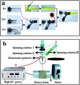 |
| | Fig. 1 Sketch maps of the preparation procedure for specially designed and installed co-axis//single-axis spinneret (a) and electrospinning equipment for fabricating [M@Lum]//E JAM (b). | |
Results and discussion
Phase
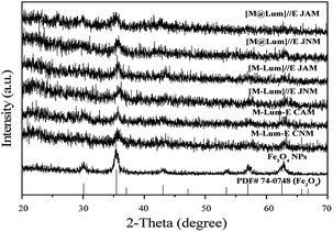
We characterized [M@Lum]//E JAM, five contrastive membranes and Fe3O4 NPs by X-ray diffractometry (Fig. 2). The XRD patterns of Fe3O4 NPs were in agreement with that of the cubic-structured of Fe3O4 (PDF 74-0748). The tests showed that all [M@Lum]//E JAM and contrastive samples contain Fe3O4 NPs.
 |
| | Fig. 2 XRD patterns of the samples with PDF standard card of Fe3O4. | |
Morphology and internal structures
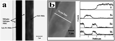
The scanning electron microscopy (SEM) images of [M@Lum]//E JAM are shown in Fig. 3a, which shows that nearly all the Janus nanobelts are configured towards the same dimension. The width of the [M@Lum]//E Janus nanobelts is ca. 6.5 μm, and the thickness is shorter than 1 μm; the results show that nearly all of the broadsides of these nanobelts are face up, which may be because this state helps the nanobelts to deposit onto the rotary drum in a much more steady manner when they are in a lower position. On the basis of the biological microscopy (BM) image analysis, the internal structure of [M@Lum]//E Janus nanobelt can be observed. A clear Janus nanobelt structure can be observed in Fig. 4a, and one side of the Janus nanobelt is [Fe3O4/PMMA]@[Tb(BA)3phen/Eu(BA)3phen/PMMA] coaxial nanobelt, which consists of a low-contrast shell and a dark-colored core; in contrast, the other side is PANI/PMMA. For further demonstration of the distinct Janus-type structure of the [M@Lum]//E Janus nanobelts, energy dispersive spectroscopy (EDS) line scan analysis was conducted (Fig. 4b); Tb, Eu, Fe and S represent Tb(BA)3phen, Eu(BA)3phen, Fe3O4 and PANI, respectively. Elemental Fe exists in the middle domain of the [Fe3O4/PMMA]@[Tb(BA)3phen/Eu(BA)3phen/PMMA] coaxial nanobelt. In addition, we found that only elemental Tb and Eu are dispersed on both sides of the coaxial nanobelt, and the other half side of the [M@Lum]//E Janus nanobelt is PANI/PMMA. Through SEM, BM, EDS line-scan analyses, we inferred that [M@Lum]//E JAM has been successfully prepared.
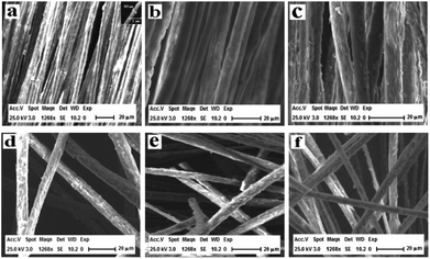 |
| | Fig. 3 SEM images of [M@Lum]//E JAM (a), [M-Lum]//E JAM (b), M-Lum-E CAM (c), [M@Lum]//E JNM (d), [M-Lum]//E JNM (e) and M-Lum-E CNM (f). | |
 |
| | Fig. 4 BM image (a) and EDS line-scan analysis (b) of a single [M@Lum]//E Janus nanobelt. | |
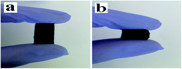
Fig. 3b and c show SEM images of [M-Lum]//E JAM and M-Lum-E CAM, respectively. As can be seen in Fig. 3b and c, the widths of each single [M-Lum]//E Janus nanobelt and M-Lum-E composite nanobelt are ca. 7.5 μm and 8 μm, respectively. In a further survey, [M-Lum]//E Janus nanobelts and M-Lum-E composite nanobelts are ordered in all samples. The SEM images of [M@Lum]//E Janus nanobelt non-array, [M-Lum]//E Janus nanobelt non-array and M-Lum-E composite nanobelt non-array are shown in Fig. 3d, e and f, respectively, whereas the Janus nanobelts and composite nanobelts are out-of-order. The widths of the independent nanobelt in [M@Lum]//E Janus nanobelt non-array, [M-Lum]//E Janus nanobelt non-array and M-Lum-E composite nanobelt non-array are ca. 8 μm, 7 μm and 5.5 μm, respectively. Fig. 5 shows typical digital photos of [M@Lum]//E JAM, and we can observe from the photos that the membrane can be easily bent and folded. This is very important for future applications of materials in flexible devices.
 |
| | Fig. 5 Digital photos of [M@Lum]//E JAM: (a) an unbent and (b) bent Janus nanobelt array membrane. | |
Fluorescent property
Luminescence performances of [M@Lum]//E JAM were studied. Color-tunable luminescence was obtained by modifying the ratios of Eu(BA)3phen to Tb(BA)3phen (samples [Sa2@Sbx]//Sc2, x = 1–5) when the mass percentage of PANI to PMMA was fixed at 30% and the mass ratio of Fe3O4 to PMMA was fixed at 1![[thin space (1/6-em)]](https://www.rsc.org/images/entities/char_2009.gif) :
:![[thin space (1/6-em)]](https://www.rsc.org/images/entities/char_2009.gif) 1. Based on previous experimental investigations,18 we chose 290 nm ultraviolet light as the excitation (abbreviated as EX) source for Tb(BA)3phen and Eu(BA)3phen compounds; under this ultraviolet light, the emission (abbreviated as EM) spectra of [M@Lum]//E JAM exhibited peaks at 490 and 545 nm, which were ascribed to the 5D4 → 7FJ (J = 6, 5) energy level transitions of Tb3+, and the peaks at 592 and 616 nm were due to the 5D0 → 7FJ (J = 1, 2) energy level transitions of Eu3+, as seen in Fig. 6 (left). The test results showed that as the mass ratio of Eu(BA)3phen to Tb(BA)3phen decreased, the green fluorescence EM of Tb3+ ions at 490 and 545 nm gradually increased, and the orange and red fluorescence EM at 592 and 615 nm of Eu3+ ions slowly decreased. Fig. 6 shows the CIE coordinates for [M@Lum]//E JAM excited by 290 nm, and the experiment verified that after adjusting the mass ratios of Eu(BA)3phen compounds to Tb(BA)3phen compounds, the fluorescence color of the samples can be adjusted from red to green.
1. Based on previous experimental investigations,18 we chose 290 nm ultraviolet light as the excitation (abbreviated as EX) source for Tb(BA)3phen and Eu(BA)3phen compounds; under this ultraviolet light, the emission (abbreviated as EM) spectra of [M@Lum]//E JAM exhibited peaks at 490 and 545 nm, which were ascribed to the 5D4 → 7FJ (J = 6, 5) energy level transitions of Tb3+, and the peaks at 592 and 616 nm were due to the 5D0 → 7FJ (J = 1, 2) energy level transitions of Eu3+, as seen in Fig. 6 (left). The test results showed that as the mass ratio of Eu(BA)3phen to Tb(BA)3phen decreased, the green fluorescence EM of Tb3+ ions at 490 and 545 nm gradually increased, and the orange and red fluorescence EM at 592 and 615 nm of Eu3+ ions slowly decreased. Fig. 6 shows the CIE coordinates for [M@Lum]//E JAM excited by 290 nm, and the experiment verified that after adjusting the mass ratios of Eu(BA)3phen compounds to Tb(BA)3phen compounds, the fluorescence color of the samples can be adjusted from red to green.
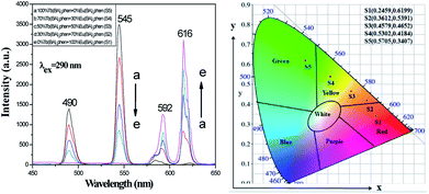 |
| | Fig. 6 EM spectra (left) and CIE chromaticity diagram (right) of [M@Lum]//E JAM containing various mass ratios of Eu(BA)3phen to Tb(BA)3phen. | |
In addition, [M@Lum]//E JAM containing various amounts of Fe3O4 NPs was fabricated to detect the influence of the addition of various amounts of Fe3O4 NPs (samples [Sax@Sb3]//Sc2, x = 1–4) on the fluorescence performances of [M@Lum]//E JAM when the mass ratio of Eu(BA)3phen to Tb(BA)3phen was set at 1![[thin space (1/6-em)]](https://www.rsc.org/images/entities/char_2009.gif) :
:![[thin space (1/6-em)]](https://www.rsc.org/images/entities/char_2009.gif) 1 and the mass percentage of PANI to PMMA was fixed at 30%, as shown in Fig. 7a. It was discovered that as the content of Fe3O4 NPs increased, the EM intensities of [M@Lum]//E JAM decreased. The results demonstrated the light absorption of Fe3O4 NPs. To explain the effect of Fe3O4 NP content on the fluorescence intensity, sketch maps of EX and EM lights in [M@Lum]//E JAM containing various mass ratios of Fe3O4 NPs to PMMA are shown in Fig. 8. Fig. 7b shows the absorption spectrum of Fe3O4 NPs. It was observed that Fe3O4 NPs can absorb visible light from 200 nm to 900 nm. Thus, the intensities of the EX and EM peaks decreased as the EX and EM lights were absorbed and weakened by Fe3O4 NPs. Fig. 7c demonstrates the CIE chromaticity diagram of [M@Lum]//E JAM with various Fe3O4 amounts under EX of 290 nm ultraviolet light. The results showed that the EM color of [M@Lum]//E JAM shifted to red with the addition of more Fe3O4 NPs, and this elaborated the theory that Fe3O4 has powerful light absorption to the light at lower wavelengths. With an increase in the amount of Fe3O4 NPs, the EM color of [M@Lum]//E JAM shifted toward red. This disclosed the fact that Fe3O4 has more powerful light absorption for light of lower wavelengths.
1 and the mass percentage of PANI to PMMA was fixed at 30%, as shown in Fig. 7a. It was discovered that as the content of Fe3O4 NPs increased, the EM intensities of [M@Lum]//E JAM decreased. The results demonstrated the light absorption of Fe3O4 NPs. To explain the effect of Fe3O4 NP content on the fluorescence intensity, sketch maps of EX and EM lights in [M@Lum]//E JAM containing various mass ratios of Fe3O4 NPs to PMMA are shown in Fig. 8. Fig. 7b shows the absorption spectrum of Fe3O4 NPs. It was observed that Fe3O4 NPs can absorb visible light from 200 nm to 900 nm. Thus, the intensities of the EX and EM peaks decreased as the EX and EM lights were absorbed and weakened by Fe3O4 NPs. Fig. 7c demonstrates the CIE chromaticity diagram of [M@Lum]//E JAM with various Fe3O4 amounts under EX of 290 nm ultraviolet light. The results showed that the EM color of [M@Lum]//E JAM shifted to red with the addition of more Fe3O4 NPs, and this elaborated the theory that Fe3O4 has powerful light absorption to the light at lower wavelengths. With an increase in the amount of Fe3O4 NPs, the EM color of [M@Lum]//E JAM shifted toward red. This disclosed the fact that Fe3O4 has more powerful light absorption for light of lower wavelengths.
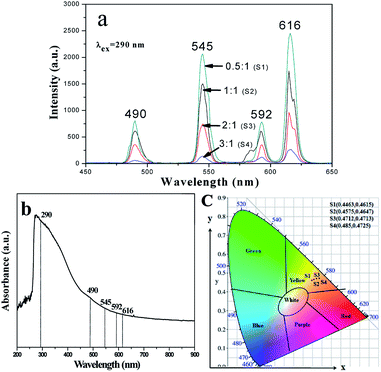 |
| | Fig. 7 EM spectra (a) and CIE chromaticity diagram (c) of [M@Lum]//E JAM containing various mass ratios of Fe3O4 NPs to PMMA; UV-vis absorption spectrum of Fe3O4 NPs (b). | |
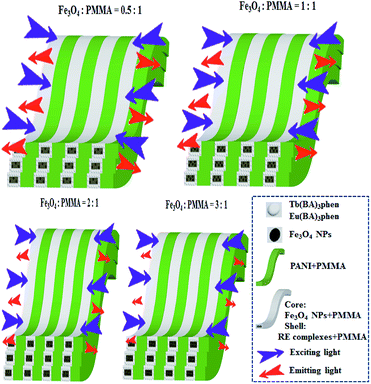 |
| | Fig. 8 Sketch maps of EX and EM light in [M@Lum]//E JAM containing various mass ratios of Fe3O4 NPs to PMMA. | |
Meanwhile, the fluorescence properties of [M@Lum]//E JAM with various amounts of PANI (samples [Sa2@Sb3]//Scx, x = 1–4) are studied when the mass ratio of Eu(BA)3phen to Tb(BA)3phen and Fe3O4 NPs to PMMA are fixed at 1![[thin space (1/6-em)]](https://www.rsc.org/images/entities/char_2009.gif) :
:![[thin space (1/6-em)]](https://www.rsc.org/images/entities/char_2009.gif) 1. As the PANI content increases, the EM intensities tend to decrease due to the light absorption of dark-colored PANI, as demonstrated in Fig. 9a. To illustrate the influence of different amounts of PANI on fluorescence, a schematic of EX and EM light in the array membrane with various percentages is shown in Fig. 10. As manifested in Fig. 9b, PANI strongly absorbs light in the range of 270–360 nm, 380–450 nm and 500–800 nm. Therefore, the EX and EM lights are absorbed by the PANI, resulting in reduced intensity of the EX and EM peaks. The CIE chromaticity coordinates for [M@Lum]//E JAM are shown in Fig. 9c. It is observed that with the introduction of PANI, the EM color of [M@Lum]//E JAM shifts to green, which is due to gradual intense absorption of red light by PANI.
1. As the PANI content increases, the EM intensities tend to decrease due to the light absorption of dark-colored PANI, as demonstrated in Fig. 9a. To illustrate the influence of different amounts of PANI on fluorescence, a schematic of EX and EM light in the array membrane with various percentages is shown in Fig. 10. As manifested in Fig. 9b, PANI strongly absorbs light in the range of 270–360 nm, 380–450 nm and 500–800 nm. Therefore, the EX and EM lights are absorbed by the PANI, resulting in reduced intensity of the EX and EM peaks. The CIE chromaticity coordinates for [M@Lum]//E JAM are shown in Fig. 9c. It is observed that with the introduction of PANI, the EM color of [M@Lum]//E JAM shifts to green, which is due to gradual intense absorption of red light by PANI.
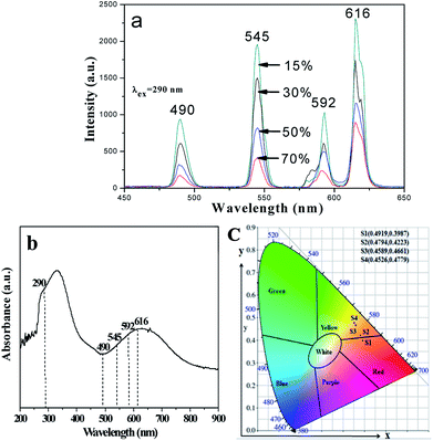 |
| | Fig. 9 EM spectra (a) and CIE chromaticity diagram (c) of [M@Lum]//E JAM containing various mass percentages of PANI to PMMA; UV-vis absorption spectrum of PANI (b). | |
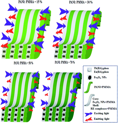 |
| | Fig. 10 Sketch maps of the EX and EM light in [M@Lum]//E JAM containing various mass percentages of PANI to PMMA. | |
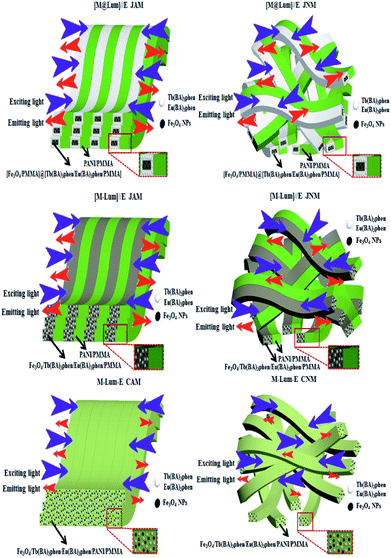
Five contrastive samples were also prepared, and their fluorescence performances were in contrast with the fluorescence performance of [M@Lum]//E JAM. As seen from Fig. 11, compared with [M@Lum]//E JAM, [M@Lum]//E JNM exhibited slightly decreased fluorescence intensity. The results also indicated that other samples had weaker fluorescence intensity when they contained the same content of raw materials. Sketch maps of the EX and EM lights in [M@Lum]//E JAM and contrastive samples are shown in Fig. 12; the figure showed that the surface of [M@Lum]//E JAM was dense because it consisted of parallel Janus nanobelts. The EX light experienced difficulty while penetrating the upper layer and reached the lower Janus nanobelts; thus, the EM light was mainly emitted from the upper Janus nanobelts without reduction. As for [M@Lum]//E JNM, the disordered Janus nanobelts led to a loose membrane surface. In this situation, part of the EX light penetrated the loose upper voids to the lower Janus nanobelts. This led to the absorption of the EX light by the upper Janus nanobelts; thus, the EX light intensity weakened. In the same manner, the EX light must go through the gap in the upper layers, which is also absorbed and attenuated. In the end, the fluorescence intensity of [M@Lum]//E JNM was lower than that of [M@Lum]//E JAM. Likewise, [M-Lum]//E JAM exhibited more powerful fluorescence intensity than [M-Lum]//E JNM, and M-Lum-E CAM exhibited stronger fluorescence intensity than M-Lum-E CNM. As is seen in Fig. 11, [M@Lum]//E JAM and JNM exhibited significantly stronger luminescence intensities than other contrastive samples. As for [M@Lum]//E JAM and JNM, the constitutional unit is the coaxial nanobelt//nanobelt ([Magnetic@Luminescent]//Electrical) type Janus nanobelt, which achieves efficient isolation of PANI and Fe3O4 NPs from RE compounds, due to which the EX and EM lights absorbed by PANI and Fe3O4 NPs are significantly reduced. For [M-Lum]//E JAM and JNM, the constitutional unit is the nanobelt//nanobelt ([Magnetic-Luminescent]//Electrical) Janus nanobelt, which also benefits the isolation of RE compounds and Fe3O4 NPs from PANI; nevertheless, the RE compounds and Fe3O4 NPs are still randomly distributed together in the Fe3O4/Tb(BA)3phen/Eu(BA)3phen/PMMA nanobelts, due to which Fe3O4 NPs absorb and weaken the EX and EM lights. In terms of M-Lum-E CAM and CNM, the constitutional unit is the (Magnetic-Luminescent-Electrical) composite nanobelt, in which the RE compounds, Fe3O4 NPs and PANI are averagely dispersed as a whole in Fe3O4/Tb(BA)3phen/Eu(BA)3phen/PANI/PMMA nanobelts, with the result that the deep-colored Fe3O4 NPs and PANI strongly absorb and weaken the EX and EM lights. The above testing results demonstrate that the [M@Lum]//E Janus-structured nanobelts with three independent partitions have better performance than [M-Lum]//E Janus-structured nanobelts with two independent partitions and M-Lum-E composite nanobelts without any partition.
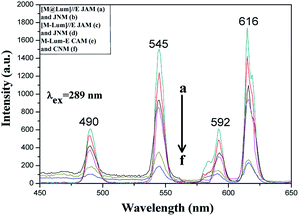 |
| | Fig. 11 EM spectra of [M@Lum]//E JAM (a) and JNM (b), [M-Lum]//E JAM (c) and JNM (d), M-Lum-E CAM (e) and CNM (f). | |
 |
| | Fig. 12 Sketch maps of EX and EM light in [M@Lum]//E JAM and contrastive samples. | |
Superparamagnetic property
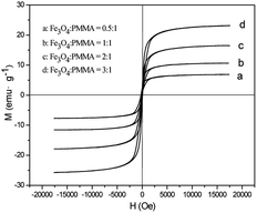
Fig. 13 shows typical hysteresis loops of [M@Lum]//E JAM containing various mass ratios of Fe3O4 NPs to PMMA. As shown in Fig. 13, the samples exhibit superparamagnetic performance. The saturation magnetizations of the samples are summarized in Table 1, and the test results show that the saturation magnetization of [M@Lum]//E JAM increases as more Fe3O4 NPs are introduced into the Fe3O4/PMMA core; this indicates that the superparamagnetism of the samples can be adjusted. In addition, as seen in Table 1, the saturation magnetizations of contrastive samples and [M@Lum]//E JAM ([Sa2@Sb3]//Sc2) are very close when they have similar components and constituents. Based on the above luminescence and magnetism test analyses, [M@Lum]//E JAM and contrastive samples have the same superparamagnetism, but [M@Lum]//E JAM has larger luminescence intensity than the contrastive samples, indicating that [M@Lum]//E JAM exhibits better performance.
 |
| | Fig. 13 Hysteresis loops of [M@Lum]//E JAM containing various mass ratios of Fe3O4 NPs to PMMA. | |
Table 1 Saturation magnetizations of [M@Lum]//E JAM containing various mass ratios of Fe3O4 to PMMA and contrastive samples
| Samples |
Saturation magnetization (Ms)/(emu g−1) |
[Sa1@Sb3]//Sc2 (Fe3O4![[thin space (1/6-em)]](https://www.rsc.org/images/entities/char_2009.gif) : :![[thin space (1/6-em)]](https://www.rsc.org/images/entities/char_2009.gif) PMMA = 0.5 PMMA = 0.5![[thin space (1/6-em)]](https://www.rsc.org/images/entities/char_2009.gif) : :![[thin space (1/6-em)]](https://www.rsc.org/images/entities/char_2009.gif) 1) 1) |
5.22 |
[Sa2@Sb3]//Sc2 (Fe3O4![[thin space (1/6-em)]](https://www.rsc.org/images/entities/char_2009.gif) : :![[thin space (1/6-em)]](https://www.rsc.org/images/entities/char_2009.gif) PMMA = 1 PMMA = 1![[thin space (1/6-em)]](https://www.rsc.org/images/entities/char_2009.gif) : :![[thin space (1/6-em)]](https://www.rsc.org/images/entities/char_2009.gif) 1) 1) |
9.67 |
[Sa3@Sb3]//Sc2 (Fe3O4![[thin space (1/6-em)]](https://www.rsc.org/images/entities/char_2009.gif) : :![[thin space (1/6-em)]](https://www.rsc.org/images/entities/char_2009.gif) PMMA = 2 PMMA = 2![[thin space (1/6-em)]](https://www.rsc.org/images/entities/char_2009.gif) : :![[thin space (1/6-em)]](https://www.rsc.org/images/entities/char_2009.gif) 1) 1) |
15.83 |
[Sa4@Sb3]//Sc2 (Fe3O4![[thin space (1/6-em)]](https://www.rsc.org/images/entities/char_2009.gif) : :![[thin space (1/6-em)]](https://www.rsc.org/images/entities/char_2009.gif) PMMA = 3 PMMA = 3![[thin space (1/6-em)]](https://www.rsc.org/images/entities/char_2009.gif) : :![[thin space (1/6-em)]](https://www.rsc.org/images/entities/char_2009.gif) 1) 1) |
23.19 |
| [M@Lum]//E JNM |
9.71 |
| [M-Lum]//E JAM |
9.53 |
| [M-Lum]//E JNM |
9.76 |
| M-Lum-E CAM |
10.11 |
| M-Lum-E CNM |
9.34 |
Electrical conduction analysis
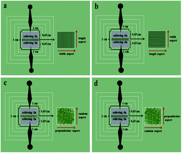
Fig. 14 shows the test methods for the electrical conduction of array (Fig. 14a and b) and non-array membranes (Fig. 14c and d). As shown in Fig. 14, two pieces of soldering tin (0.45 cm in width and 1 cm in length) are placed on the specimen (the specimen is cut into 1 cm × 1 cm); then, the two pins of the Hall effect measurement system are connected to the two pieces of soldering tin. For the array membranes, the conductance along the length and width of the nanobelts in the membranes can be determined. For the non-array membranes, the conductance along a random dimension (equivalent to length) and the corresponding perpendicular dimension (equivalent to width) can be measured. The electrical properties of [M@Lum]//E with various amounts of PANI (samples [Sa2@Sb3]//Scx, x = 1–4) are measured, and the determined conductance values and ratios between length and width are listed in Table 2. From Table 2, it can be seen that the conductance of these array membranes can be tuned by adjusting the mass percentage of PANI to PMMA, and the conductance along the length of the [M@Lum]//E Janus nanobelts in the array membrane sharply increases from 6.24 × 10⁻⁷ S to 4.41 × 10⁻² S when the mass percentage of PANI to PMMA changes from 15% to 70%. The conductance along the width dimension retains ca. 10 orders of magnitude, resulting in a high conductance ratio between length and width. Besides, this shows that the conductance along the length is ca. 8 orders of magnitude higher than that along the width when the mass percentage of PANI is fixed at 70%, which proves that [M@Lum]//E JAM has strong anisotropy in electrical conduction; as far as we know, the volume is the largest conductance ratio between the two perpendicular directions for nanobelt membrane. The results show that [M@Lum]//E JAM is electrically conducting only along the length and insulative along the width, and the Janus nanobelts have electrically conducting anisotropy that can be adjusted by varying the PANI content.
 |
| | Fig. 14 Test methods for electrical conduction along the length (a) and width (b) of the nanobelts in array membrane and along the random dimension (c) and perpendicular dimension (d) in non-array membrane. | |
Table 2 Conductance volumes and anisotropy degree of [M@Lum]//E JAM
| Samples |
Length direction (S) |
Width direction (S) |
Ratio of length direction to width direction |
Anisotropic degree |
| [Sa2@Sb3]//Sc1 (PANI/PMMA: 15%) |
6.24 × 10⁻⁷ |
2.48 × 10⁻¹⁰ |
2.52 × 10³ |
Medium |
| [Sa2@Sb3]//Sc2 (PANI/PMMA: 30%) |
8.33 × 10⁻⁶ |
1.17 × 10⁻¹⁰ |
7.12 × 10⁴ |
Medium |
| [Sa2@Sb3]//Sc3 (PANI/PMMA: 50%) |
5.75 × 10⁻⁴ |
3.24 × 10⁻¹⁰ |
1.77 × 10⁶ |
Strong |
| [Sa2@Sb3]//Sc4 (PANI/PMMA: 70%) |
4.41 × 10⁻² |
1.79 × 10⁻¹⁰ |
2.46 × 10⁸ |
Very strong |
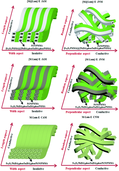
Conductance and electrically conducting anisotropy of the [M@Lum]//E JAM and contrastive samples were comparatively studied when the mass percentage of PANI to PMMA was set to 30%, as seen in Table 3 and Fig. 15. In Table 3, the ratio of length to width in [M-Lum]//E JAM is 1.34 × 10⁴, which is similar to that of [M@Lum]//E JAM (7.12 × 10⁴), implying that both have strong anisotropy. In contrast, composite nanobelt array membranes only have weak electrically conducting anisotropy (5.43 × 101). Fig. 15 shows the sketch maps for the electrical properties of [M@Lum]//E JAM and contrastive samples. In [M@Lum]//E JAM and [M-Lum]//E JAM, electrons can flux along the length of the Janus nanobelts without obstacles and are obstructed along the width owing to the presence of insulative [M@Lum] or [M-Lum] nanobelts, resulting in a higher conductance ratio between the two perpendicular dimensions of the two types of membranes. Compared with [M@Lum]//E JAM and [M-Lum]//E JAM, M-Lum-E CAM has significantly lower electrically conducting anisotropy. On the one hand, the electrically conducting unit is the PANI/PMMA nanobelt in [M@Lum]//E JAM and [M-Lum]//E JAM, which achieves efficient isolation of insulative RE compounds and Fe3O4 NPs from conducting PANI and guarantees the high conductance along the length of the Janus nanobelts. Nevertheless, the electrically conducting unit is Fe3O4/Tb(BA)3phen/Eu(BA)3phen/PANI/PMMA nanobelts in M-Lum-E CAM, which prevents the building of a continuous PANI conducting network and reduces the conductance of the composite nanobelts. As seen in Table 3, the conductance values along the length of [M@Lum]//E JAM and [M-Lum]//E JAM are higher than that along the length of M-Lum-E CAM. On the other hand, there are no effective insulative units among the nanobelts in M-Lum-E CAM; only the interfaces between the composite nanobelts can be used as a less effective insulating medium and thus, the conductance along the width of the nanobelts in M-Lum-E CAM is higher than that along the width in [M@Lum]//E JAM and [M-Lum]//E JAM. In brief, the insulating performance along the width of the nanobelts in M-Lum-E CAM is not strong enough. As shown in Table 3, the non-array membranes have negligible electrically conducting anisotropy. As show in Fig. 15, because the nanobelts in [M-Lum]//E JNM and M-Lum-E CNM are disordered in arrangement, the direction of current flow is disordered, which leads to electrically conducting isotropy of these non-array membranes. Under these circumstances, because electrical conduction exists in all directions of the membrane, the volume of conductance decreases in a particular dimension. From what has been discussed above, we can conclude that two key requirements must be met in the preparation of highly conducting anisotropic films. The other is that the insulator unit will be used and inserted into the insulating direction of the array film to further block the movement of electrons.
Table 3 Conductance volumes of [M@Lum]//E JAM and contrastive samples
| Samples |
Length direction (S) |
Width direction (S) |
Ratio of length direction to width direction |
Anisotropic degree |
| [M@Lum]//E JAM |
8.33 × 10⁻⁶ |
1.17 × 10⁻¹⁰ |
7.12 × 10⁴ |
Strong |
| [M@Lum]//E JNM |
7.07 × 10⁻⁷ |
6.28 × 10⁻⁷ |
1.13 |
None |
| [M-Lum]//E JAM |
7.42 × 10⁻⁶ |
5.51 × 10⁻¹⁰ |
1.34 × 10⁴ |
Strong |
| [M-Lum]//E JNM |
9.02 × 10⁻⁸ |
9.67 × 10⁻⁸ |
0.93 |
None |
| M-Lum-E CAM |
5.59 × 10⁻⁷ |
1.03 × 10⁻⁸ |
5.43 × 101 |
Weak |
| M-Lum-E CNM |
4.47 × 10⁻⁸ |
4.22 × 10⁻⁸ |
1.06 |
None |
 |
| | Fig. 15 Sketch maps of electrical conduction in [M@Lum]//E JAM and contrastive samples. | |
In combination with the above fluorescence analysis, superparamagnetism and electrically conducting anisotropy, we are pleased to discover that the fluorescence intensity of [M@Lum]//E JAM is much stronger than that of [M-Lum]//E JAM when they have similar magnetism and electrically conducting anisotropy, proving that the new [M@Lum]//E JAM have better luminescent-superparamagnetic-electrical properties than [M-Lum]//E JAM. The [M@Lum]//E Janus nanobelts with three isolated partitions are superior in structuring multifunctional nanomaterials as compared with the [M-Lum]//E Janus nanobelts with two isolated partitions and M-Lum-E composite Janus nanobelts without any partition.
Thermal stability analysis
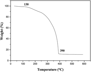
The TG curve for [M@Lum]//E JAM is shown in Fig. 16. [M@Lum]//E JAM loses about 1.31% of its initial weight when the temperature is increased from room temperature to 130 °C due to volatilization of surface absorbed water. With the continuous increase in temperature, organic compounds such as Tb(BA)3phen, Eu(BA)3phen, PMMA and PANI start to decompose, and the decomposition process is completed at 390 °C. The total weight loss percentage is 87.83%. These results show that [M@Lum]//E JAM can be safely applied below 130 °C.
 |
| | Fig. 16 TG curve of [M@Lum]//E JAM. | |
Conclusions
In summary, we have established a new method to construct novel and brand-new flexible peculiar-structured [coaxial nanobelt]//[nanobelt] Janus nanobelts, which are very different from already-reported [nanobelt]//[nanobelt] structure type Janus nanobelts, via electrospinning technology using a newly-designed and manufactured co-axis//single-axis spinneret. With the aid of the peculiar-structured [coaxial nanobelt]//[nanobelt] Janus nanobelts, luminescent, magnetic and electrical substances are mutually isolated, and mutual interferences among them can be further reduced, due to which excellent tri-functionalities of luminescence, electricity and magnetism are concurrently integrated into the Janus nanobelts. Additionally, from the microcosmic angle, partition of only two isolated functional domains can be realized by using the already-reported common 1D Janus nanobelt; nevertheless, partition of three isolated functional domains rather than two isolated functional domains is successfully realized in the new 1D Janus nanobelt reported in this study. Therefore, the novel Janus nanobelts can also be extended to assemble various three functions to realize multi-functionalization without reducing mutual interferences. Furthermore, the peculiar-structured [coaxial nanobelt]//[nanobelt] Janus nanobelts are used to build anisotropic conductive array membranes. Because [Fe3O4/PMMA]@[Tb(BA)3phen/Eu(BA)3phen/PMMA] as insulative units are inserted into the insulative portion of the array membranes, which further blocks the movement of electrons, the largest conductivity ratio between the length and width directions of the nanobelts in the array membrane reaches up to eight orders of magnitude, which is the highest conductivity ratio between the two perpendicular dimensions for nanobelt membranes. Moreover, the electrically conducting anisotropy of Janus nanobelt array membranes can be tuned by adjusting the amount of PANI. Besides, the Janus nanobelt array membrane is simultaneously endued with tunable superparamagnetism and color-tunable fluorescence. The design philosophy and the construction technique for the novel Janus nanobelts and array membranes can afford a facile approach for the fabrication of Janus nanobelts and array membranes with other tri- or multi-functionalities.
Conflicts of interest
There are no conflicts of interest to declare.
Acknowledgements
This work was financially supported by National Natural Science Foundation of China (51573023, 50972020), Natural Science Foundation of Jilin Province (20170101101JC, 20180520011JH), Industrial Technology Research and Development Project of Jilin Province Development and Reform Commission (2017C052-4), Science and Technology Research Planning Project of the Education Department of Jilin Province during the 13th five-year plan period (JJKH20170608KJ, JJKH20181122KJ), and Innovative Foundation (XJJLG-2017-04) and Youth Foundation (XQNJJ-2016-01, XQNJJ-2017-17) of Changchun University of Science and Technology.
References
- N. I. Kovtyukhova and T. E. Mallouk, J. Phys. Chem. B, 2005, 109, 2540–2545 CrossRef PubMed.
- C. Feng, K. Liu, J. S. Wu, L. Liu, J. S. Cheng, Y. Y. Zhang, Y. H. Sun, Q. Q. Li, S. S. Fan and K. L. Jiang, Adv. Funct. Mater., 2010, 20, 885–891 CrossRef.
- J. R. Huang, Y. T. Zhu, W. Jiang and Q. X. Tang, ACS Appl. Mater. Interfaces, 2014, 6, 1754–1758 CrossRef PubMed.
- W. A. D. Heer, A. Chatelain and D. Ugarte, Science, 1995, 270, 1179–1181 CrossRef.
- Q. L. Ma, J. X. Wang, X. T. Dong, W. S. Yu and G. X. Liu, Adv. Funct. Mater., 2015, 25, 2436–2443 CrossRef.
- Q. L. Ma, W. S. Yu, X. T. Dong, M. Yang, J. X. Wang and G. X. Liu, Sci. Rep., 2015, 5, 14583 CrossRef PubMed.
- L. Han, M. M. Pan, Y. Lv, Y. T. Gu, X. F. Wang, D. Li, Q. L. Kong and X. T. Dong, J. Mater. Sci.: Mater. Electron., 2015, 26, 677–684 CrossRef.
- X. Xi, Q. L. Ma, M. Yang, X. T. Dong, J. X. Wang, W. S. Yu and G. X. Liu, J. Mater. Sci.: Mater. Electron., 2014, 25, 4024–4032 CrossRef.
- J. Tian, Q. L. Ma, W. S. Yu, X. T. Dong, Y. Yang, B. Zhao, J. X. Wang and G. X. Liu, New J. Chem., 2017, 41, 13983–13992 RSC.
- X. B. Li, Q. L. Ma, J. Tian, X. Xi, D. Li, X. T. Dong, W. S. Yu, X. L. Wang, J. X. Wang and G. X. Liu, Nanoscale, 2017, 9, 18918–18930 RSC.
- K. Lun, Q. L. Ma, M. Yang, X. T. Dong, Y. Yang, J. X. Wang, W. S. Yu and G. X. Liu, J. Mater. Sci.: Mater. Electron., 2015, 26, 5994–6003 CrossRef.
- Q. L. Ma, J. X. Wang, X. T. Dong, W. S. Yu and G. X. Liu, Chem. Eng. J., 2013, 222, 16–22 CrossRef.
- H. Shao, Q. L. Ma, X. T. Dong, W. S. Yu, M. Yang, J. X. Wang and G. X. Liu, Phys. Chem. Chem. Phys., 2015, 17, 21845–21855 RSC.
- Q. L. Ma, J. X. Wang, X. T. Dong, W. S. Yu and G. X. Liu, Nanoscale, 2014, 6, 2945–2952 RSC.
- X. Xi, J. X. Wang, X. T. Dong, Q. L. Ma, W. S. Yu and G. X. Liu, Chem. Eng. J., 2014, 254, 259–267 CrossRef.
- X. Xi, Q. L. Ma, X. T. Dong, D. Li, W. S. Yu, J. X. Wang and G. X. Liu, J. Mater. Sci.: Mater. Electron., 2018, 29, 7119–7129 CrossRef.
- K. Lun, Q. L. Ma, M. Yang, X. T. Dong, Y. Yang, J. X. Wang, W. S. Yu and G. X. Liu, Chem. Eng. J., 2015, 279, 231–240 CrossRef.
- J. Tian, Q. L. Ma, X. T. Dong, M. Yang, Y. Yang, J. X. Wang, W. S. Yu and G. X. Liu, J. Mater. Sci.: Mater. Electron., 2015, 26, 8413–8420 CrossRef.
Footnote |
| † Electronic supplementary information (ESI) available. See DOI: 10.1039/c8ra06283h |
|
| This journal is © The Royal Society of Chemistry 2018 |
Click here to see how this site uses Cookies. View our privacy policy here.  Open Access Article
 *ab,
Jinxian Wang
 a and
Guixia Liu
 a
a


![[thin space (1/6-em)]](https://www.rsc.org/images/entities/char_2009.gif) :
:![[thin space (1/6-em)]](https://www.rsc.org/images/entities/char_2009.gif) 1. Based on previous experimental investigations,18 we chose 290 nm ultraviolet light as the excitation (abbreviated as EX) source for Tb(BA)3phen and Eu(BA)3phen compounds; under this ultraviolet light, the emission (abbreviated as EM) spectra of [M@Lum]//E JAM exhibited peaks at 490 and 545 nm, which were ascribed to the 5D4 → 7FJ (J = 6, 5) energy level transitions of Tb3+, and the peaks at 592 and 616 nm were due to the 5D0 → 7FJ (J = 1, 2) energy level transitions of Eu3+, as seen in Fig. 6 (left). The test results showed that as the mass ratio of Eu(BA)3phen to Tb(BA)3phen decreased, the green fluorescence EM of Tb3+ ions at 490 and 545 nm gradually increased, and the orange and red fluorescence EM at 592 and 615 nm of Eu3+ ions slowly decreased. Fig. 6 shows the CIE coordinates for [M@Lum]//E JAM excited by 290 nm, and the experiment verified that after adjusting the mass ratios of Eu(BA)3phen compounds to Tb(BA)3phen compounds, the fluorescence color of the samples can be adjusted from red to green.
1. Based on previous experimental investigations,18 we chose 290 nm ultraviolet light as the excitation (abbreviated as EX) source for Tb(BA)3phen and Eu(BA)3phen compounds; under this ultraviolet light, the emission (abbreviated as EM) spectra of [M@Lum]//E JAM exhibited peaks at 490 and 545 nm, which were ascribed to the 5D4 → 7FJ (J = 6, 5) energy level transitions of Tb3+, and the peaks at 592 and 616 nm were due to the 5D0 → 7FJ (J = 1, 2) energy level transitions of Eu3+, as seen in Fig. 6 (left). The test results showed that as the mass ratio of Eu(BA)3phen to Tb(BA)3phen decreased, the green fluorescence EM of Tb3+ ions at 490 and 545 nm gradually increased, and the orange and red fluorescence EM at 592 and 615 nm of Eu3+ ions slowly decreased. Fig. 6 shows the CIE coordinates for [M@Lum]//E JAM excited by 290 nm, and the experiment verified that after adjusting the mass ratios of Eu(BA)3phen compounds to Tb(BA)3phen compounds, the fluorescence color of the samples can be adjusted from red to green.

![[thin space (1/6-em)]](https://www.rsc.org/images/entities/char_2009.gif) :
:![[thin space (1/6-em)]](https://www.rsc.org/images/entities/char_2009.gif) 1 and the mass percentage of PANI to PMMA was fixed at 30%, as shown in Fig. 7a. It was discovered that as the content of Fe3O4 NPs increased, the EM intensities of [M@Lum]//E JAM decreased. The results demonstrated the light absorption of Fe3O4 NPs. To explain the effect of Fe3O4 NP content on the fluorescence intensity, sketch maps of EX and EM lights in [M@Lum]//E JAM containing various mass ratios of Fe3O4 NPs to PMMA are shown in Fig. 8. Fig. 7b shows the absorption spectrum of Fe3O4 NPs. It was observed that Fe3O4 NPs can absorb visible light from 200 nm to 900 nm. Thus, the intensities of the EX and EM peaks decreased as the EX and EM lights were absorbed and weakened by Fe3O4 NPs. Fig. 7c demonstrates the CIE chromaticity diagram of [M@Lum]//E JAM with various Fe3O4 amounts under EX of 290 nm ultraviolet light. The results showed that the EM color of [M@Lum]//E JAM shifted to red with the addition of more Fe3O4 NPs, and this elaborated the theory that Fe3O4 has powerful light absorption to the light at lower wavelengths. With an increase in the amount of Fe3O4 NPs, the EM color of [M@Lum]//E JAM shifted toward red. This disclosed the fact that Fe3O4 has more powerful light absorption for light of lower wavelengths.
1 and the mass percentage of PANI to PMMA was fixed at 30%, as shown in Fig. 7a. It was discovered that as the content of Fe3O4 NPs increased, the EM intensities of [M@Lum]//E JAM decreased. The results demonstrated the light absorption of Fe3O4 NPs. To explain the effect of Fe3O4 NP content on the fluorescence intensity, sketch maps of EX and EM lights in [M@Lum]//E JAM containing various mass ratios of Fe3O4 NPs to PMMA are shown in Fig. 8. Fig. 7b shows the absorption spectrum of Fe3O4 NPs. It was observed that Fe3O4 NPs can absorb visible light from 200 nm to 900 nm. Thus, the intensities of the EX and EM peaks decreased as the EX and EM lights were absorbed and weakened by Fe3O4 NPs. Fig. 7c demonstrates the CIE chromaticity diagram of [M@Lum]//E JAM with various Fe3O4 amounts under EX of 290 nm ultraviolet light. The results showed that the EM color of [M@Lum]//E JAM shifted to red with the addition of more Fe3O4 NPs, and this elaborated the theory that Fe3O4 has powerful light absorption to the light at lower wavelengths. With an increase in the amount of Fe3O4 NPs, the EM color of [M@Lum]//E JAM shifted toward red. This disclosed the fact that Fe3O4 has more powerful light absorption for light of lower wavelengths.

![[thin space (1/6-em)]](https://www.rsc.org/images/entities/char_2009.gif) :
:![[thin space (1/6-em)]](https://www.rsc.org/images/entities/char_2009.gif) 1. As the PANI content increases, the EM intensities tend to decrease due to the light absorption of dark-colored PANI, as demonstrated in Fig. 9a. To illustrate the influence of different amounts of PANI on fluorescence, a schematic of EX and EM light in the array membrane with various percentages is shown in Fig. 10. As manifested in Fig. 9b, PANI strongly absorbs light in the range of 270–360 nm, 380–450 nm and 500–800 nm. Therefore, the EX and EM lights are absorbed by the PANI, resulting in reduced intensity of the EX and EM peaks. The CIE chromaticity coordinates for [M@Lum]//E JAM are shown in Fig. 9c. It is observed that with the introduction of PANI, the EM color of [M@Lum]//E JAM shifts to green, which is due to gradual intense absorption of red light by PANI.
1. As the PANI content increases, the EM intensities tend to decrease due to the light absorption of dark-colored PANI, as demonstrated in Fig. 9a. To illustrate the influence of different amounts of PANI on fluorescence, a schematic of EX and EM light in the array membrane with various percentages is shown in Fig. 10. As manifested in Fig. 9b, PANI strongly absorbs light in the range of 270–360 nm, 380–450 nm and 500–800 nm. Therefore, the EX and EM lights are absorbed by the PANI, resulting in reduced intensity of the EX and EM peaks. The CIE chromaticity coordinates for [M@Lum]//E JAM are shown in Fig. 9c. It is observed that with the introduction of PANI, the EM color of [M@Lum]//E JAM shifts to green, which is due to gradual intense absorption of red light by PANI.


![[thin space (1/6-em)]](https://www.rsc.org/images/entities/char_2009.gif) :
:![[thin space (1/6-em)]](https://www.rsc.org/images/entities/char_2009.gif) PMMA = 0.5
PMMA = 0.5![[thin space (1/6-em)]](https://www.rsc.org/images/entities/char_2009.gif) :
:![[thin space (1/6-em)]](https://www.rsc.org/images/entities/char_2009.gif) 1)
1)![[thin space (1/6-em)]](https://www.rsc.org/images/entities/char_2009.gif) :
:![[thin space (1/6-em)]](https://www.rsc.org/images/entities/char_2009.gif) PMMA = 1
PMMA = 1![[thin space (1/6-em)]](https://www.rsc.org/images/entities/char_2009.gif) :
:![[thin space (1/6-em)]](https://www.rsc.org/images/entities/char_2009.gif) 1)
1)![[thin space (1/6-em)]](https://www.rsc.org/images/entities/char_2009.gif) :
:![[thin space (1/6-em)]](https://www.rsc.org/images/entities/char_2009.gif) PMMA = 2
PMMA = 2![[thin space (1/6-em)]](https://www.rsc.org/images/entities/char_2009.gif) :
:![[thin space (1/6-em)]](https://www.rsc.org/images/entities/char_2009.gif) 1)
1)![[thin space (1/6-em)]](https://www.rsc.org/images/entities/char_2009.gif) :
:![[thin space (1/6-em)]](https://www.rsc.org/images/entities/char_2009.gif) PMMA = 3
PMMA = 3![[thin space (1/6-em)]](https://www.rsc.org/images/entities/char_2009.gif) :
:![[thin space (1/6-em)]](https://www.rsc.org/images/entities/char_2009.gif) 1)
1)
