
 Open Access Article
 This Open Access Article is licensed under a Creative Commons Attribution-Non Commercial 3.0 Unported Licence
Tunable bandwidth of double electromagnetic induced transparency windows in terahertz graphene metamaterial
Yue Wang,
Mengning Tao,
Zhen Pei,
Xuzheng Yu,
Benhua Wang,
Jiuxing Jiang and
Xunjun He *
*
School of Science, Harbin University of Science and Technology, No. 52 Xuefu Road, Nangang District, Harbin, Heilongjiang 150080, P. R. China. E-mail: hexunjun@hrbust.edu.cn
First published on 5th November 2018
Abstract
By patterning graphene on a SiO2/Si substrate, in this paper, we design and numerically investigate double electromagnetic induced transparency (EIT) windows in a terahertz metamaterial based on a π-like graphene structure. The surface current distributions reveal that the double EIT windows arise from the destructive interferences caused by different asymmetric coupling modes. Moreover, the bandwidth of two transparency windows can be actively controlled by changing the asymmetric coupling strength. By shifting the Fermi energy of graphene, more interestingly, the bandwidth and frequency modulation depths of the two transparency windows is 38.4% and 36% respectively, and the associated group delay and delay bandwidth product (DBP) can also be actively tuned. Therefore, such EIT-like graphene metamaterials are promising candidates for designing slow-light devices and wide-band filters.
1. Introduction
Recently, the metamaterial-based electromagnetically induced transparency analogue has attracted considerable attention owing to a promising a variety of potential applications, such as slow-light devices,1 sensing,2 and novel optical communication systems, and quantum information storages.3 Usually, such EIT-like effect obtained in metamaterials arises from the destructive interference between bright and dark modes or superradiant and subradiant modes.4 Currently, different EIT-like terahertz metamaterials have been reported and experimentally demonstrated through these two approaches.5–7 By changing the distance between two resonators of the unit cell or by exciting active materials integrated into the unit cell utilizing electricity or light, moreover, their transparency windows can be actively tuned.8–11 Unfortunately, most of these EIT-like metamaterials normally localize the transparency window in a narrow spectral range, which will significantly limit the scope of the EIT-like metamaterial applications.12 Therefore, the EIT-like metamaterials with tunable bandwidth are important for the future applications in the terahertz frequency regime. However, only a few broadband EIT-like metamaterials have been reported so far.13–15Since being discovered in 2004, graphene has attracted extensive interests due to its unique properties.16–18 More importantly, the graphene conductivity can be dynamically tuned by doping.19 Currently, different graphene metamaterials have been designed and demonstrated by patterning or stacking graphene structures to realize various functional or tunable devices.20–28 Therefore, the graphene metamaterials would open up new approaches for actively controlling the bandwidth of the EIT window. Motivated by the above fundamental studies, in this paper, we design and characterize a simple graphene metamaterial structure to realize two EIT windows. Moreover, we demonstrated numerically that the bandwidth and working frequency of the transparency window are dynamically tuned by changing the strength of the asymmetric coupling or Fermi energy of graphene. Therefore, such EIT-like graphene metamaterials designed here are promising candidates for developing slow-light devices and wide-band filters.
2. Designs and simulations of structure
In this paper, we designed a double-EIT metamaterial based on the π-like graphene array patterned on the low-doped SiO2/Si substrate acting as back gate, as shown in Fig. 1(a). The unit cell of the designed EIT metamaterial can be decomposed into two asymmetric T-shaped structures composed of same horizontal graphene wire and vertical graphene cut-wires with different lengths respectively, as shown in Fig. 1(b) and (c). Moreover, the horizontal wires of all unit cells are connected with two metallic pads to form top gate. Thus, the graphene can be actively doped by applying a bias voltage between the top and back gates to change the Fermi energy of graphene (see Fig. 1(a)), as experimentally demonstrated in previous reports.29,30 Compared to the traditional metal-based EIT structures, therefore, the most arresting feature of this structure is that the bandwidth and working region of two transparency windows can be actively controlled by changing the strength of the asymmetric coupling or Fermi energy of graphene. | ||
| Fig. 1 The designed double EIT graphene metamaterial: (a) schematic of graphene metamaterial, (b) π-like unit cell structure, and (c) asymmetric T-shaped structure. | ||
In order to explore electromagnetic response of the designed graphene-based metamaterial, numerical calculations based on finite difference time domain (FDTD) method are carried out. In the simulations, the moderate mesh accuracy is adopted to make good tradeoff between accuracy, memory requirements and simulation time. Thus, a time step of 1645 fs and the highest mesh accuracy are set in our simulations. The periodic boundary conditions are used for a unit cell in x- and y-directions, and the perfectly matched layer boundary condition is applied in z-plane. The plane wave polarizing along x-direction is normally incident to the structure surface along z-direction, as shown in Fig. 1(a). In the numerical calculations, the structural parameters are as following: a = 100 μm, l = 70 μm, d = 28 μm and w = 4 μm. The relative permittivities of the SiO2 layer and Si substrate are taken as 3.9 and 11.7 respectively, and their corresponding thicknesses are 30 nm and 300 μm respectively. While, the graphene is assumed to be an effective medium with thickness of tg = 0.34 nm and the relative complex permittivity of εr(ω) = 1 + jσ(ω)/(ωε0tg), in which the conductivity σ(ω) can be described as:31
 | (1) |
3. Results and discussions
3.1 Single transparency window
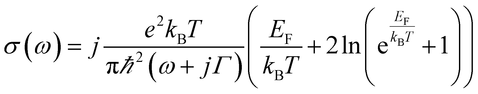
Before studying the π-like array structure as shown in Fig. 1(b), we start by investigating an asymmetric T-shaped structure shown in Fig. 1(c). As observed in Fig. 2(a), a tiny transparency window can be observed in the transmission spectrum once the symmetry of the T-shaped structure is broken. If further enhancing asymmetric coupling by increasing the horizontal displacement s, a sharp transparency window will appear in the transmission spectrum, which is the typical EIT window observed in the EIT system.32,33 To better understand the occurrence of the transparency window, the surface currents at the transmission dip A1 and the transparency peak A2 marked in Fig. 2(a) are calculated, and the corresponding calculated results are shown in Fig. 2(b). For the transmission dip A1, the inphase currents on the surfaces of two back-to-back L-shaped structures are excited due to strongly coupling with the incident wave. Thus, the resonance mode can act as the bright mode because of large radiative losses. For the transparency peak A2, however, the antiphase surface currents on two L-shaped structures are excited due to the asymmetric coupling, leading to a cancellation of the surface currents in the vertical graphene cut-wire and a large current oscillation along the horizontal graphene wire, which indicates that the dark mode is excited in the horizontal graphene wire. As a result, a sharp transparency window is induced due to the destructive interference between the bright and dark modes. | ||
| Fig. 2 Transmission properties and current distributions of the asymmetric T-shaped structure for different horizontal displacement s: (a) simulated transmission curves and (b) simulated surface currents. | ||
The above EIT behavior can be further understood by the classical coupled two-oscillator systems,34
 | (2) |
 | ||
| Fig. 3 Transmission spectra and fitting parameters for different horizontal displacement s: (a) comparison of the simulated and theoretical results, and (b) the fitting parameters γ1, γ2, δ and κ as the functions of the horizontal displacement s. | ||
As demonstrated above, breaking structural symmetry can induce the transparency window, as shown in Fig. 2. Next, we would further investigate the effect of the geometrical parameter l on the transparency window. As observed in Fig. 4(a), when the length of the vertical cur-wire decreases from 70 μm to 40 μm (from top to bottom), the transmission dip at higher frequency shows obvious blue-shift and the corresponding dip depth remains almost unchanged, while the transmission dip at lower frequency shows slight blue-shift, but the corresponding dip depth becomes smaller, indicating a weaker resonance. As a result, the obvious transparency peak disappears between two transmission dips due to weak near field coupling between the horizontal wire and vertical cut-wire of the asymmetric T-shaped structure. This behavior can be explained by the surface current distributions at four transmission dips A, B, C, and D shown in Fig. 4(a). As shown in Fig. 4(b) and (c), the transmission dips A, B and D have similar surface current distributions, which mainly focus on the L-shaped structure. This result indicates that these resonances come from the same origin. For the transmission dip C, however, the surface currents focus mainly on the horizontal graphene wire, which is similar to the dark mode. Therefore, the lower resonance gradually weakens with increasing l, as shown in Fig. 4(a).
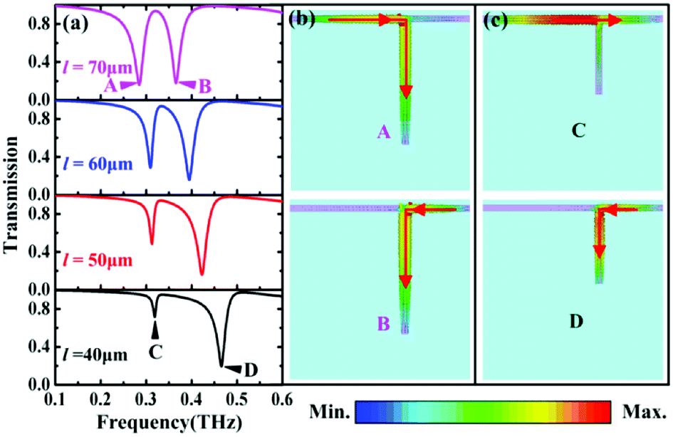 | ||
| Fig. 4 Transmission spectra and surface currents of the asymmetric T-shaped metamaterial with different l: (a) transmission spectra for different length, (b) surface currents at transmission dips A and B, and (c) surface currents at transmission dips C and D. | ||
3.2 Double transparency windows
For the traditional more EIT-based system, usually, multiple transparency windows can be obtained by integrating more dark and bright modes into a unit cell or nesting several structures with close enough resonance frequency together.36,37 Moreover, such system is highly desirable in many practical applications.38 Here, we demonstrate that two transparency windows can be achieved in the designed π-like structure shown in Fig. 1(b). To clarify underlying forming process of the two transparency windows, the transmission spectra of two isolated asymmetric T-shaped structures with the vertical cut-wires of different lengths are also given. As observed in Fig. 5(a), when two isolated asymmetric T-shaped structures are combined together to form a π-like structure, a new transparency window appears between two high frequency transmission dips (H and J) of two isolated T-shaped structures due to introducing new asymmetric coupling, while the positions and strength of the three original transmission dips (F, H and J) and the original transparency window (G) generated respectively by two isolated structures remain almost unchanged. | ||
| Fig. 5 (a) Calculated transmission spectra of three different graphene metamaterials: isolated shorter asymmetric T-shaped graphene array for l = 30 μm (bottom row), isolated longer asymmetric T-shaped graphene array for l = 70 μm (middle row) and combined π-like structure (top row), (b) surface current distributions of the combined π-like structure at three transmission dips (A, D and E) and two transparency peaks (B and D), (c) surface current distributions of the isolated shorter asymmetric T-shaped structure at two transmission dips (F and H) and the transparency peak (G), and (d) surface current distributions of the isolated shorter asymmetric T-shaped structure at two transmission dips (I and J). | ||
To better understand the occurrence mechanism of two transparency windows, the surface currents at the transmission dips and the transparency peaks shown in Fig. 5(a) are calculated, respectively. As observed, the surface current distributions at the transparency peak (B) and three transmission dips (A, C and E) shown in Fig. 5(b) are completely similar to that of the transparency peak (G) and three transmission dips (F, H and J) shown in Fig. 5(c) and (d), which indicates that the corresponding resonant behaviour comes from same origin. For the transparency peak (D), however, the antiphase surface currents on two different L-shaped structures are excited due to asymmetric coupling between two vertical graphene cut-wires, exhibiting similar field distributions of the quadrupole, thus, a new dark mode is excited. From the induced surface current distributions on the π-like structure, therefore, it can be inferred that the two transparency windows come from two different destructive interferences caused respectively by the asymmetric coupling between the horizontal graphene wire and the vertical graphene cut-wire and between two vertical graphene cut-wires with different lengths.
As demonstrated above, two transparency windows are excited due to introducing different asymmetric coupling modes. Next, we further investigate the effect of the asymmetric coupling on the bandwidth of two transparency windows by changing the geometrical parameters of the unit cell structure. The transmission spectra for different structural parameters Δl and d shown in Fig. 1(b) are calculated respectively. As observed in Fig. 6(a), with the increase of the length deviation Δl between two vertical cut-wires (from bottom row to top row), two transmission dips at lower frequencies are slightly blue-shifted and the corresponding resonant depths become larger, indicating stronger resonances, while the third transmission dip at the highest frequency is obviously blue-shifted and the corresponding dip depth remains almost unchanged, as a result, leading to two sharp transparency windows. Moreover, the bandwidth of two transparency windows gradually widens with increase in Δl. This can be attributed to the strong asymmetric coupling between two vertical cut-wires, as demonstrated in the surface current distributions of Fig. 5(b). As increasing the separation d between two vertical cut-wires (from bottom to top), in addition, the first transmission dip remains almost unchanged, the middle transmission dip is slightly blue-shifted and the corresponding resonant depth becomes gradually larger, while the third transmission dip exhibits obvious blue-shift (as shown in Fig. 6(b)). Thus, the bandwidth of two transparency windows gradually widens. Once again, this can be explained by strong asymmetric coupling between the horizontal wire and the vertical cut-wire. Therefore, the bandwidth of two transparency windows induced in this structure can be actively controlled by changing asymmetric coupling strength.
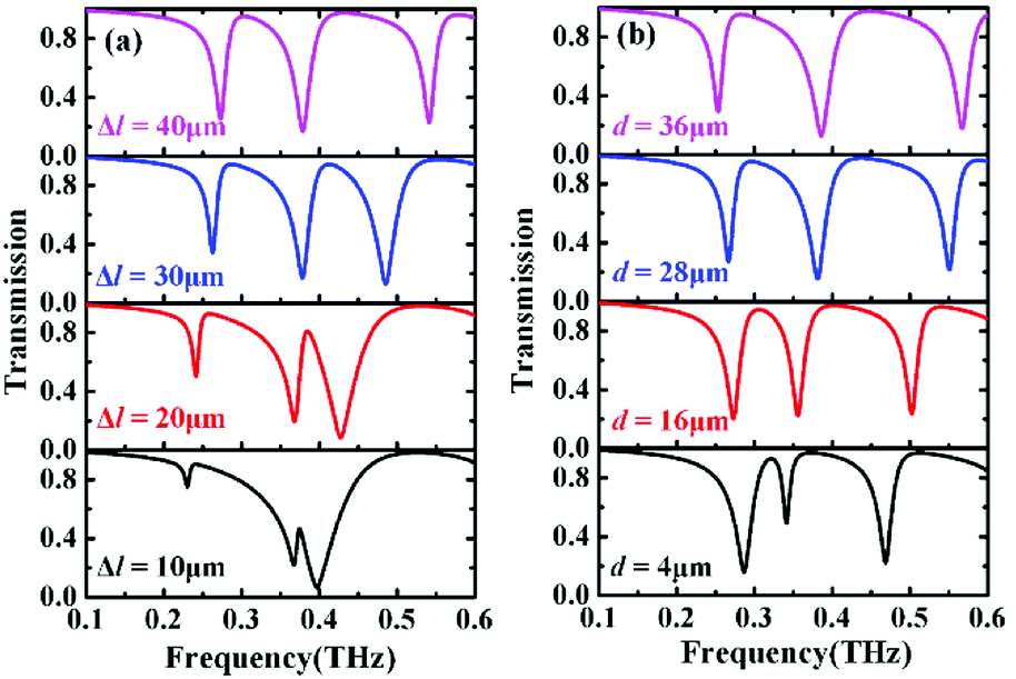 | ||
| Fig. 6 Effect of the structural parameters on the transmission spectra: (a) different length deviation between two vertical cut-wires and (b) different separation between two vertical cut-wires. | ||
3.3 Tunability
Compared with the traditional metal-based metamaterials, the most obvious advantage of the graphene metamaterials is active reconfiguration and tuning, which is highly desirable in many practical applications.38 To further explore the modulation capacity of the designed graphene metamaterial, the transmission spectra of the designed π-like structure with different Fermi energy are calculated. As shown in different colour regions of Fig. 7(a), two transparency windows show obvious blue-shift as increase in Fermi energy of graphene, and the similar change has been experimentally demonstrated in previous reports.39,40 As a result, it can be found that the frequency modulation depth (fmod = Δf/fmax) of both two transparency peaks is about 36% when the Fermi energy changes in the range of 0.08–0.3 eV. If the Fermi energy further increases, better tunable properties can be obtained, as observed in the previous results.41,42 Simultaneously, it is also noted that the resonant strength of the π-like structure is enhanced as the Fermi energy increases. These behaviors can be attributed to change in resonant frequency of graphene cut-wire, in which the resonant frequency can be written as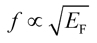 .38,43 During the blue-shift, moreover, the amplitude of the transparency peak is almost unchanged, while the corresponding bandwidth gradually widens, as shown in Fig. 7(b). In another word, when Fermi energy changes from 0.08 eV to 0.3 eV, the bandwidth of two windows (different colour region of Fig. 7(a)) increases from 202 GHz to 328 GHz, and the corresponding bandwidth modulation depth is 38.4%. Based on the blue-shift response, in addition, the designed π-like structure can realize the switching function in the interested frequency range. Such as, the transmission amplitude can switch between 0.263 and 0.947 at 0.32 THz as the Fermi energy changes between 0.08 eV and 0.12 eV, or between 0.945 and 0.082 at 0.40 THz as Fermi energy changes between 0.2 eV to 0.3 eV, and the corresponding magnitude modulation depths are 72% and 91%, respectively. Therefore, the working frequency and bandwidth of two transparency windows can be actively controlled by varying Fermi energy of graphene.
 | ||
| Fig. 7 (a) Blue-shift and (b) bandwidth of two transparency windows in the proposed π-like metamaterial with various values of Fermi energy from 0.08 eV to 0.3 eV. | ||
3.4 Group delay
As well known, a remarkable characteristic of EIT-like response is strong phase dispersion in transparent window region, which can reduce the group velocity.44 As observed in Fig. 8(a), the designed π-like structure exhibits a sudden phase jump in two transparency window regions, in which a steep slope can be obtained. Meanwhile, we also notice that the transmission phase spectrum has two frequency segments: normal phase dispersion and abnormal phase dispersion. The normal dispersion, which leads to a significantly enhanced group delay, occurs in the transparent window, while the abnormal dispersion (not discussed here) occurs around the plasmonic resonance. As increase in Fermi energy, moreover, the corresponding normal phase dispersion experiences a strong change and becomes more and more obvious. This phenomenon can be attributed to the change in the coupling strength between graphene cut-wires.45,46 Therefore, these results indicate that our structure can actively control slow light.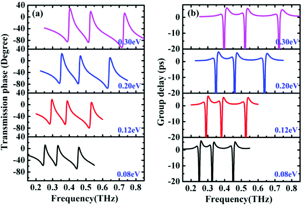 | ||
| Fig. 8 Phase dispersion and group delay of the proposed graphene metamaterial for various Fermi energy EF: (a) simulated transmission phase and (b) corresponding group delay. | ||
To examine the capacity of controlling slow light, the group delay is calculated by the expression: τg = −dφ/dω, where φ and ω = 2πf are the phase shift and frequency of transmission spectrum, respectively.47,48 Fig. 8(b) shows the calculated group delays of the designed π-like structure with different Fermi energy. As expected, the large positive group delay can be achieved in the sharp dispersion region due to the excitation of the transparency window, which leads to strong slow light effect. As increase in Fermi energy from 0.08 eV to 0.3 eV, moreover, the region of the group delay exhibits clear blue-shift over a fairly wide frequency range and widens obviously, which is similar to the change in the transmission spectrum shown in Fig. 7(a). In addition, we also notice the negative group delays at the nearby regions of the two transparency windows, indicating fast light effect, as experimentally observed in atomic EIT systems or EIT-like metamaterials.49
For the practical application in slow light device, however, only talking about group delay is meaningless. Meanwhile, we should also consider the bandwidth of group delay. Generally, the delay bandwidth product (DBP) is used to describe the highest slow light capacity range that the device potentially provides.50 Here, the DBP is defined as the product of the maximum group delay and spectrum bandwidth (DBP = τg × Δf), where Δf is the full width at half maximum bandwidth (FWHM), τg is the maximum group delay at the transparency window.51 For the designed π-like metamaterial structure, we find that as increase in Fermi energy from 0.08 eV to 0.3 eV, the DBPs of two transparency windows increase from 0.357 to 0.571 and from 0.536 to 0.948, respectively. Therefore, the DBP and working region of the slow light effect can be also actively controlled by changing Fermi energy of graphene.
4. Conclusions
In summary, the actively controlled bandwidth and working region of two transparency windows in a terahertz metamaterial based on the π-like graphene array have been numerically demonstrated in this paper. The surface currents reveal that two transparency windows arise from the destructive interferences caused by two different asymmetric coupling modes. Further investigations demonstrate that the bandwidths of two transparency windows can be dynamically controlled by changing the asymmetric coupling strength. As increase in Fermi energy of graphene from 0.08 eV to 0.3 eV, more importantly, two transparency windows can realize the bandwidth modulation depth of 38.4% and the frequency modulation depth of 36%. In addition, the associated group delay and DBP can be also actively tuned. Therefore, the designed EIT metamaterials are promising candidates in a variety of applications for developing tunable slow-light devices and wide-band filters.Conflicts of interest
There are no conflicts to declare.Acknowledgements
The work is supported by the National Natural Science Foundation of China (51672062, 51575149 and 51402075), Project of Innovative and Entrepreneurship Training Program for College students in Heilongjiang Province (201810214105).References
- V. Kravtsov, J. M. Atkin and M. B. Raschke, Opt. Lett., 2013, 38, 1322 CrossRef PubMed.
- R. Singh, W. Cao, I. Al-Naib, L. Cong, W. Withayachumnankul and W. Zhang, Appl. Phys. Lett., 2014, 105, 171101 CrossRef.
- R. Taubert, M. Hentschel, J. Kästel and H. Giessen, Nano Lett., 2012, 12, 1367 CrossRef CAS PubMed.
- Z. H. Zhu, X. Yang, J. Q. Gu, J. Jiang, W. S. Yue, Z. Tian, M. Tonouchi, J. G. Han and W. L. Zhang, Broadband plasmon induced transparency in terahertz metamaterials, Nanotechnology, 2013, 24, 214003 CrossRef PubMed.
- S. Y. Chiam, R. Singh, C. Rockstuhl, F. Lederer, W. L. Zhang and A. A. Bettiol, Phys. Rev. B, 2009, 80, 153103 CrossRef.
- S. X. Li, H. W. Zhao and J. G. Han, J. Electron. Sci. Technol., 2015, 13, 117 Search PubMed.
- Z. Liao, S. Liu, H. F. Ma, C. Li, B. B. Jin and T. J. Cui, Sci. Rep., 2016, 6, 27596 CrossRef CAS PubMed.
- J. Liu, J. Q. Gu, R. Singh, Y. F. Ma, J. Zhu, Z. Tian, M. X. He, J. G. Han and W. L. Zhang, Appl. Phys. Lett., 2012, 100, 131101 CrossRef.
- J. Gu, R. Singh, X. Liu, X. Zhang, Y. Ma, S. Zhang, S. A. Maier, Z. Tian, A. K. Azad, H. T. Chen, A. J. Taylor, J. H. Han and W. L. Zhang, Nat. Commun., 2012, 3, 1151 CrossRef PubMed.
- P. Pitchappa, M. Manjappa, C. P. Ho, R. Singh, N. Singh and C. Lee, Adv. Opt. Mater., 2016, 4, 541 CrossRef CAS.
- Y. C. Fan, T. Qiao, F. L. Zhang, Q. H. Fu, J. J. Dong, B. T. Kong and H. Q. Li, Sci. Rep., 2017, 7, 40441 CrossRef CAS PubMed.
- Y. Wang, Y. B. Leng, L. Wang, L. H. Dong, S. R. Liu, J. Wang and Y. J. Sun, Appl. Phys. Express, 2018, 11, 062001 CrossRef.
- C. Wu, A. B. Khanikaev and G. Shvets, Phys. Rev. Lett., 2011, 106, 107403 CrossRef PubMed.
- S. Han, H. L. Yang and L. Y. Guo, J. Appl. Phys., 2013, 114(16), 163507 CrossRef.
- R. Yahiaoui, M. Manjappa, Y. K. Srivastava and R. Singh, Appl. Phys. Lett., 2017, 111, 021101 CrossRef.
- K. S. Novoselov, V. I. Fal’ko, L. Colombo, P. R. Gellert, M. G. Schwab and K. Kim, Nature, 2012, 490, 192 CrossRef CAS PubMed.
- X. Xu, Q. Q. Zhang, Y. K. Yu, W. L. Chen, H. Hu and H. Li, Adv. Mater., 2016, 28, 9223 CrossRef CAS PubMed.
- Q. Q. Zhang, X. Xu, D. Lin, W. L. Chen, G. P. Xiong, Y. K. Yu, T. S. Fisher and H. Li, Adv. Mater., 2016, 28, 2229 CrossRef CAS PubMed.
- A. Vakil and N. Engheta, Science, 2011, 332, 1291 CrossRef CAS PubMed.
- Y. Fan, Z. Liu, F. Zhang, Q. Zhao, Z. Wei, Q. Fu, J. Li, C. Gu and H. Li, Sci. Rep., 2015, 5, 13956 CrossRef CAS PubMed.
- Y. C. Fan, N. H. Shen, T. Koschny and C. M. Soukoulis, ACS Photonics, 2015, 2(1), 151–156 CrossRef CAS.
- H. Cheng, S. Q. Chen, P. Yu, W. W. Liu, Z. C. Li, J. X. Li, B. Y. Xie and J. G. Tian, Adv. Opt. Mater., 2015, 3(12), 1744–1749 CrossRef CAS.
- X. Y. He, Carbon, 2015, 82, 229 CrossRef CAS.
- S. X. Xia, X. Zhai, L. L. Wang, B. Sun, J. Q. Liu and S. C. Wen, Opt. Express, 2016, 24(15), 17886 CrossRef CAS PubMed.
- Y. P. Zhang, T. T. Li, Q. Chen, H. Y. Zhang, J. F. O'Hara, E. Abele, A. J. Taylor, H. T. Chen and A. K. Azad, Sci. Rep., 2015, 5, 18463 CrossRef CAS PubMed.
- X. Y. He, P. Q. Gao and W. Z. Shi, Nanoscale, 2016, 8, 10388–10397 RSC.
- S. X. Xia, X. Zhai, L. L. Wang and S. C. Wen, Photonics Res., 2018, 6(7), 692 CrossRef.
- X. Y. He, F. Liu, F. T. Lin and W. Z. Shi, Opt. Express, 2018, 26, 9931–9944 CrossRef PubMed.
- F. Valmorra, G. Scalari, C. Maissen, W. Y. Fu, C. Schönenberger, J. W. Choi, H. G. Park, M. Beck and J. Faist, Nano Lett., 2013, 13(7), 3193 CrossRef CAS PubMed.
- P. Q. Liu, I. J. Luxmoore, S. A. Mikhailov, N. A. Savostianova, F. Valmorra, J. Faist and G. R. Nash, Nat. Commun., 2015, 6, 8969 CrossRef CAS PubMed.
- B. Vasic, M. M. Jakovljevic, G. Isic and R. Gajic, Appl. Phys. Lett., 2013, 103, 011102 CrossRef.
- X. B. Zheng, Z. Y. Zhao, W. Z. Shi and W. Peng, Opt. Mater. Express, 2017, 7(3), 1035–1047 CrossRef CAS.
- N. Liu, T. Weiss, M. Mesch, L. Langguth, U. Eigenthaler, M. Hirscher, C. Sonnichsen and H. Giessen, Nano Lett., 2010, 10, 1103–1107 CrossRef CAS PubMed.
- N. Liu, T. Weiss, J. Kästel, M. Fleischhauer, T. Pfau and H. Giessen, Nat. Mater., 2009, 8, 758–762 CrossRef CAS PubMed.
- T. Koschny, P. Markoš, E. N. Economou, D. R. Smith, D. C. Vier and C. M. Soukoulis, Phys. Rev. B, 2005, 7, 1245105 Search PubMed.
- X. G. Yin, T. H. Feng, S. P. Yip, Z. X. Liang, A. Hui, J. C. Ho and J. Li, Appl. Phys. Lett., 2013, 103, 021115 CrossRef.
- F. Bagci and B. Akaoglu, J. Appl. Phys., 2017, 122, 073103 CrossRef.
- J. Ding, B. Arigong, H. Ren, M. Zhou, J. Shao, M. Lu, Y. Chai, Y. Lin and H. Zhang, Sci. Rep., 2014, 4, 6128 CrossRef CAS PubMed.
- L. Ju, B. S. Geng, J. Horng, C. Girit, M. Martin, Z. Hao, H. A. Bechtel, X. G. Liang, A. Zettl, Y. R. Shen and F. Wang, Nat. Nanotechnol., 2011, 6, 630–634 CrossRef CAS PubMed.
- D. Rodrigo, O. Limaj, D. Janner, D. Etezadi, F. J. Abajo, V. Pruneri and H. Altug, Science, 2015, 349, 165–168 CrossRef CAS PubMed.
- X. Y. He, F. T. Lin, F. Liu and W. Z. Shi, Nanotechnology, 2016, 27, 485202 CrossRef PubMed.
- Y. P. Zhang, T. T. Li, B. B. Zeng, H. Y. Zhang, H. H. Lv, X. Y. Huang, W. L. Zhang and A. K. Azad, Nanoscale, 2015, 7, 12682 RSC.
- J. X. Jiang, Q. F. Zhang, Q. X. Ma, S. T. Yan, F. M. Wu and X. J. He, Opt. Mater. Express, 2015, 5, 1962–1971 CrossRef CAS.
- W. Cao, R. Singh, C. H. Zhang, J. G. Han, M. Tonouchi and W. L. Zhang, Appl. Phys. Lett., 2013, 103, 101106 CrossRef.
- B. Tang, L. Dai and C. Jiang, Opt. Express, 2011, 19(2), 628 CrossRef CAS PubMed.
- J. Q. Wang, B. H. Yuan, C. Z. Fan, J. N. He, P. Ding, Q. Z. Xue and E. J. Liang, Opt. Express, 2013, 21(21), 25159 CrossRef PubMed.
- T. Zentgraf, S. Zhang, R. F. Oulton and X. Zhang, Phys. Rev. B, 2009, 80(19), 195415 CrossRef.
- L. Zhang, P. Tassin, T. Koschny, C. Kurter, S. M. Anlage and C. M. Soukoulis, Appl. Phys. Lett., 2010, 97(24), 241904 CrossRef.
- Z. Y. Zhao, Z. Q. Song, W. Z. Shi and W. Peng, Opt. Mater. Express, 2016, 6, 2190 CrossRef CAS.
- T. Baba, Nat. Photonics, 2008, 2(8), 465–473 CrossRef CAS.
- X. G. Yin, T. H. Feng, S. Yip, Z. X. Liang, A. Hui, J. C. Ho and J. Li, Appl. Phys. Lett., 2013, 103(2), 021115 CrossRef.
| This journal is © The Royal Society of Chemistry 2018 |