
 Open Access Article
 This Open Access Article is licensed under a Creative Commons Attribution-Non Commercial 3.0 Unported Licence
AFM-thermoreflectance for simultaneous measurements of the topography and temperature†
Jinsung Rho‡
,
Mikyung Lim‡,
Seung S. Lee and
Bong Jae Lee *
*
Department of Mechanical Engineering, Korea Advanced Institute of Science and Technology, Daejeon 34141, South Korea. E-mail: bongjae.lee@kaist.ac.kr
First published on 2nd August 2018
Abstract
To understand the thermal failure mechanisms of electronic devices, it is essential to measure the temperature and characterize the thermal properties of individual nanometer-scale transistors in electronic devices. Previously, scanning thermal microscopy (SThM) has been used to measure the local temperature with nanometer-scale spatial resolutions using a probe with a built-in temperature sensor. However, this type of temperature measurement requires additional equipment to process the temperature-sensing signals and expensive temperature-sensor-integrated probes fabricated by complicated MEMS processes. Here, we present a novel technique which enables the simultaneous measurement of the temperature and topography of nanostructures only with a conventional atomic force microscope (AFM) of the type commonly used for topography measurements and without any modifications of the probe and extra accessories for data acquisition. The underlying principle of the proposed technique is that the local temperature of a specimen is estimated quantitatively from the thermoreflectance of a bare silicon AFM probe that is in contact with a specimen. The temperature obtained by our technique is found to be consistent with a result obtained by SThM measurements.
1 Introduction
Nanoscale thermometry is an essential technique in diverse research areas, such as micro/nano electronics, thermophysical properties of nanomaterials, and thermoelectric energy conversion.1–16 As an example, the failure of an integrated electronic device can be caused by a hot spot in a transistor which in turn deteriorates the performance and reliability of electronic devices.1,17 Accordingly, the need to understand thermal transport on the sub-100 nm scale, which is comparable to the width of the fine electrodes in a transistor, necessitates the development of a temperature-sensing method with a sub-100 nm spatial resolution.1,13–16,18–27 Further, nanoscale thermometry with a high spatial resolution is paramount for accurate thermal characterizations of nanomaterials (e.g., graphene, carbon nanotubes, or nanowires), which have recently drawn enormous amounts of attention.11–14,27–34 Related research has been carried out with micro-Raman spectroscopy,35 thermoreflectance (TR),36–40 near-field scanning optical microscopy (NSOM),41 scanning thermal microscopy (SThM),12–14,18–24,30–34,42–46 and other measurement methods. However, it should be noted that micro-Raman and TR methods are limited in terms of their ability to measure temperature with sub-100 nm spatial resolutions due to the optical diffraction limit.To meet the demands of nanoscale thermometry with sub-100 nm resolutions, recent studies focus on scanning probe-based thermometries.1,13,14,18–25,30–34,41,47 Among these technique, in the case of NSOM which measures temperature in near-field,41 the spatial resolution is determined by the size of the probe aperture. Accordingly, it requires a very small aperture as well as a complex optical system for high spatial resolutions. Also, SThM, which is contact nanothermometry based on the atomic force microscope (AFM) platform, employs a temperature-sensing probe.1,6 In order to obtain the temperature distribution on the sample surface, the resistance change of a conductor embedded in a probe13,14,20,21,30 or the thermoelectric voltage generated at a thermocouple junction placed at the tip end of a probe18,19,22–24,31–34 must be measured, meaning that an additional system is required to process the signal. Further, these temperature-sensor-integrated probes are produced through a complex MEMS fabrication process, making them expensive and fragile. Consequently, the complexity of both the system and the probe limits the broader application of those techniques with regard to the sensing of nanoscale temperature distributions.
In this work, we propose a novel form of AFM-based thermometry capable of sub-100 nm spatial resolutions. Without using a temperature-sensor-inserted probe, the local temperature on a specimen can be measured by exploiting the TR characteristic (i.e., the change of the reflectance with respect to the temperature) of a conventional AFM Si probe, whose temperature is determined by the heat transfer from the specimen that is in contact with the probe. A key advantage of our technique is that temperature measurements with sub-100 nm spatial resolutions are possible with only a low-cost AFM Si probe without any accessories. The laser diode used for the topography measurement in conventional AFM can also be used as a light source for TR measurement. Moreover, a quadrant photo detector (QPD) of the type found in a conventional AFM can also be employed to detect the change of the laser intensity reflected from the Si probe, enabling TR measurements with a conventional AFM alone. Here, the temperature image with a sub-100 nm spatial resolution will be obtained with a conventional AFM (NTEGRA Aura, NT-MDT) and a conventional Si probe (RESP10, Bruker) with the proposed AFM-TR technique. Quantitative temperature measurements are achieved through calibration, as in previous works with SThM.23,31 Further, the measured temperature will be compared with that obtained with a commercially available SThM probe (NP SThM 02, TSP Nanoscopy) to demonstrate the validity of the proposed technique.
2 Results and discussion
2.1 Concept of the AFM-TR technique
The conventional AFM system consisting of an AFM probe, a QPD, and a laser diode is depicted in Fig. 1. The QPD is divided into the quadrant sections of four photodiodes, denoted here as A, B, C, and D. When the tip of the probe scans the sample surface, the cantilever of the probe is deflected according to the topography of the sample surface. The corresponding change in the laser signal reflected on the cantilever results in variation of the detected laser signal in each of four photodiodes. The changes in the signal detected by each diode are converted into topography information in the conventional AFM system.6 To be specific, while scanning the surface of the sample, a topography image is obtained from the difference between the signals from the upper part and the lower part of the QPD while the frictional force between the probe tip and the sample surface can be estimated from the difference between the signals from the left side and the right side of the QPD.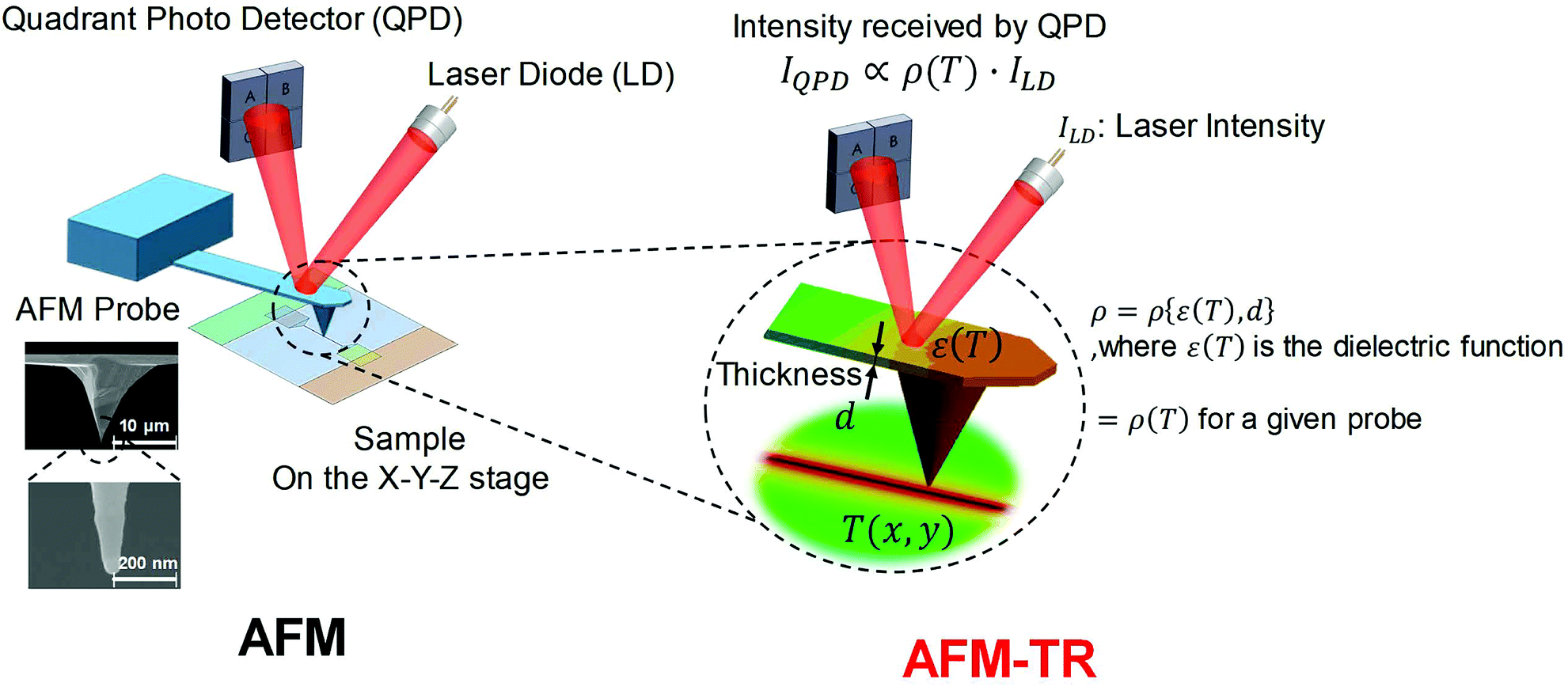 | ||
| Fig. 1 Concept of the AFM-TR technique. In a conventional AFM set up, the laser beam is emitted from the laser diode, reflected on the probe cantilever, and measured on the QPD. The difference between the signals from the upper part and the lower part of the QPD is used to produce a topography image. The AFM-TR technique exploits the total sum of the QPD signal which is proportional to the probe cantilever (Si) reflectance which can be varied by the local temperature of the sample surface. | ||
If the temperature distribution of the sample is not uniform, the temperature of the cantilever, onto which the laser beam is irradiated, is also varied according to the local temperature of the sample surface due to the heat transfer at the tip–sample contact point. Thus, the change in the reflected laser signal depending on the temperature of the cantilever (i.e., thermoreflectance) can be used to estimate the change in the temperature of the sample. Considering an actual AFM configuration, the difference between the signals from the upper and the lower parts of the QPD can be used to obtain a topography image, while the sum of signals from all quadrants A, B, C, and D (i.e., the total detected laser signal) can be used to deduce the reflectance of the Si probe. In general, the reflectance of the cantilever (ρ) depends on the dielectric function (ε) and the thickness (d) of the cantilever, the wavelength of the incident laser beam (λ) and the incident angle of the laser beam (θ). Here, the dielectric function is again a function of the incident laser beam wavelength and temperature of the material. Consequently, if the thickness of the cantilever and wavelength and angle of the incident laser beam are kept constant, the reflectance is then only a function of the temperature of the cantilever. Because the temperature-dependent dielectric function of Si, which is widely used as an AFM probe material, is well characterized,36,38–40 thermometry is possible with the TR characteristics of the conventional AFM Si probe. This method is termed the AFM-TR technique (Fig. 1). Again, key to enabling the AFM-TR is the fact that the laser signal reflected on the Si cantilever can be used not only for topography measurements but also for the thermoreflectance measurement.
2.2 Experimental results
To demonstrate the AFM-TR technique, a tungsten line heater is fabricated. As part of this step, 1 μm-thick SiO2 film is thermally grown on a Si substrate as an thermal insulation layer and the tungsten line heater is patterned onto it with electron-beam lithography. A topography image of the fabricated sample obtained via AFM is shown in Fig. 2a. The measured line width and height of the tungsten line heater are 1.19 μm and 40 nm, respectively. The length of the line heater is designed to be 80 μm. Throughout the paper, all measurements are conducted under a low-vacuum condition (∼2 mTorr) to suppress the parasitic heat transfer between the AFM probe and the sample in the form of air conduction/convection and the conduction through the liquid meniscus at the tip–sample contact point.1,19,48 A current output module (NI 9265, National Instruments) and a voltage input module (NI 9223, National Instruments) were used to supply current to the tungsten line heater and to measure voltage difference across the heater, respectively. A field-programmable gate-array (FPGA) embedded controller (NI cRIO 9039, National Instruments) was introduced to control the modules and calculate the electrical resistance of the tungsten line heater. | ||
| Fig. 2 Effect of the topography and sample temperature on the relative change of QPD signal. (a) Topography of the sample and (b) ΔQPDR when the temperature distribution of the sample is uniform (i.e., room temperature). (c) ΔQPDR measured with respect to the input power applied to the tungsten line heater at point (1), denoted with a circular mark, and at point (2), denoted with a square-shaped mark. Inset of (c): a topography image of the tungsten line heater and the contact points where the measurements were conducted. | ||
The total QPD signal from quadrants A, B, C, and D can be expressed as 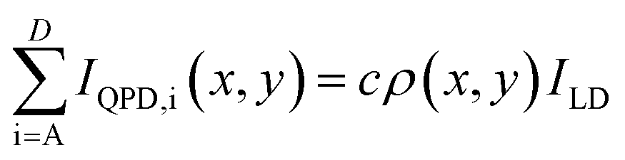 , where the coordinate (x, y) refers to the contact point between the AFM tip and the sample surface (see Fig. 2a). Here, IQPD,i indicates the laser signal obtained from each quadrant of the QPD, where ρ is the reflectance of the AFM cantilever, c is a constant value, and ILD is the intensity of the laser beam irradiated from the laser diode. When calculating the total sum of the QPD signals, the constant c is necessary to compensate for the loss caused by the size difference between the incident laser beam and the cantilever. That is, only a certain portion of the laser beam irradiated onto the cantilever is reflected on the cantilever (i.e., c ≤ 1). In order to measure the temperature while scanning over the heater, the change in the total QPD signal can be defined as
 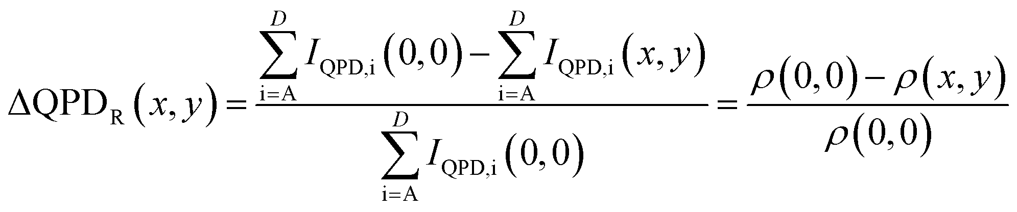 , where the point (0, 0) is the initial scanning location. By taking the relative change of the total QPD signal between two points (i.e., one at desired location and the other at reference location), the unknown constant c and the incident laser beam intensity ILD do not need to be known.
For the AFM-TR technique to be considered as a reliable temperature-measuring technique, two criteria should be met. The first is that the total QPD signal should not be affected by the sample topography, and the second is that the total QPD signal should be a monotonic function of the sample surface temperature. First, in order to examine how the total QPD signal is related to the topography, images of the topography and the total QPD signal are obtained simultaneously for the tungsten-line-heater sample maintained at room temperature (see Fig. 2a and b). Fig. 2a is obtained from the difference between the signals from the upper and the lower parts of the QPD (i.e., the topography image) and Fig. 2b plots the relative change in the total QPD signal (i.e., ΔQPDR) while scanning the sample surface as it is held at room temperature. Because heating power is not applied to the tungsten line heater, it can be safely assumed that both the heater and the probe are in a state of thermal equilibrium at room temperature. In contrast to the clear topography image of the tungsten line heater shown in Fig. 2a, there is no noticeable distribution of ΔQPDR (see Fig. 2b); that is, ΔQPDR is decoupled with the topography of the sample. In this measurement, it can be confirmed that the total QPD signal is not a function of the topography and that ΔQPDR remains at an average of 0.02% with a standard deviation of 0.0067%. A detailed discussion of the noise in ΔQPDR and the corresponding temperature resolution will be presented later in relation to the sensitivity of the Si probe.
The dependence of ΔQPDR on the temperature of the sample surface can be revealed by measuring ΔQPDR while heating the tungsten line heater via Joule heating. Given that the increase in the local temperature of the sample is proportional to the Joule heating power applied to the tungsten line heater, ΔQPDR is measured with respect to the power input. Here, ΔQPDR is defined as the relative change in the total QPD signal with respect to the initial total QPD signal (i.e., when heating power is not applied to the heater) at a certain point. Because the total QPD signal is independent of the topography when there is no temperature distribution (see Fig. 2b), the total QPD signal at any point before Joule heating can be safely used as the reference point. As shown in the inset of Fig. 2c, the AFM probe tip is brought into contact with the midpoint of the tungsten line heater (denoted as point 1) and the SiO2 film (denoted as point 2) which is positioned 1 μm away from point 1. ΔQPDR obtained at each point while increasing the Joule heating power from 0 mW to 15 mW is plotted in Fig. 2c. It is clear that ΔQPDR at both points increases with an increase in the input power and that ΔQPDR is higher at the point on the tungsten line heater than it is at the point on the SiO2. These results verify that ΔQPDR is a function of the local temperature of the sample. To be specific, ΔQPDR increases with respect to the local temperature of the sample monotonically as well as linearly (see Fig. 2c). Such monotonic and linear TR characteristics are possible because the increase in the temperature of the AFM probe is minute compared to that on the surface of the sample (∼60 K at 15 mW as will be shown later). In fact, if we compare ΔQPDR to the outcome with previously reported Si TR,39 ΔQPDR obtained in this study has a much smaller value. The nanoscopic tip–sample contact required for a high spatial resolution inevitably results in considerable thermal contact resistance. Accordingly, thermal equilibrium between the probe cantilever and the sample surface cannot be achieved, and the temperature rise in the AFM probe cantilever should be much smaller than that on the sample surface, leading to low sensitivity when using this technique. On the other hand, such a small temperature rise of the probe due to large contact resistance can be beneficial, as monotonic and linear TR characteristics of a Si probe are possible in a relatively narrow temperature range. Further, bending or expansion of the Si probe at a high temperature, which also affects the QPD signal and increases the uncertainty, can be avoided in cases involving such small temperature increases of the probe. The low sensitivity arising due to the nanoscopic tip–sample contact, which is, however, advantageous in terms of the spatial resolution and TR performance, can be mitigated with high sensitivity of the TR measurements.
In order to demonstrate that the AFM-TR technique can be used for quantitative temperature measurements, calibration with a reference sample was conducted to determine the relationship between ΔQPDR and the local temperature on the tungsten line heater. Because the thermal contact resistance at the contact point between the probe tip and the sample surface is a function of the degrees of thermal conductivity of the tip and the sample,1,23 a reference tungsten-line-heater sample (i.e., same material with the actual sample) is introduced.31 A detailed explanation of the calibration processes is provided in ESI.† The sensitivity of ΔQPDR to the temperature of the tungsten line heater was found to be 0.013% K−1, where the validity of the calibration process is confirmed through a finite element method (FEM) simulation (see ESI†).
Using the calibrated Si probe, a quantitative temperature measurement with the proposed AFM-TR technique is demonstrated. In Fig. 3, the temperature distributions estimated from ΔQPDR(x) while heating the tungsten line heater via Joule heating at input power levels of 3.01 mW, 9.29 mW and 19.17 mW are depicted. As expected, Fig. 3 clearly indicates that the local temperature increases with an increase in the input power. Further, because the input power applied to the heater is dissipated from the heater to the surrounding 1 μm-thick SiO2 film, the maximum temperature should be obtained at the midpoint of the tungsten line heater, which is also observable in Fig. 3. For comparison, the temperature measured with the AFM-TR technique and the calculation results obtained from a FEM simulation with ANSYS software are plotted as well (see ESI†). The temperature profiles from the FEM simulation are slightly different from the experimental results, which may be due to the fact that the trapezoidal cross-section of the actual tungsten line heater is assumed to be rectangular in the FEM model. Nevertheless, the experimental results generally are in good agreement with the predicted results, except for the temperature profiles at the edge. The sharp temperature change at the edge, which is a non-physical jump of the measured temperature, is due to an abrupt change in the contact resistance between the tip and the tungsten line heater. At this point, the contact between the heater edge and the side plane of the probe tip leads to an increase in the contact area, resulting in a fictitious temperature jump at the edge. This phenomena is frequently found in previous works with SThM,22,23 and it can be offset through the two-pass method14 or through a dynamic adjustment.24,45
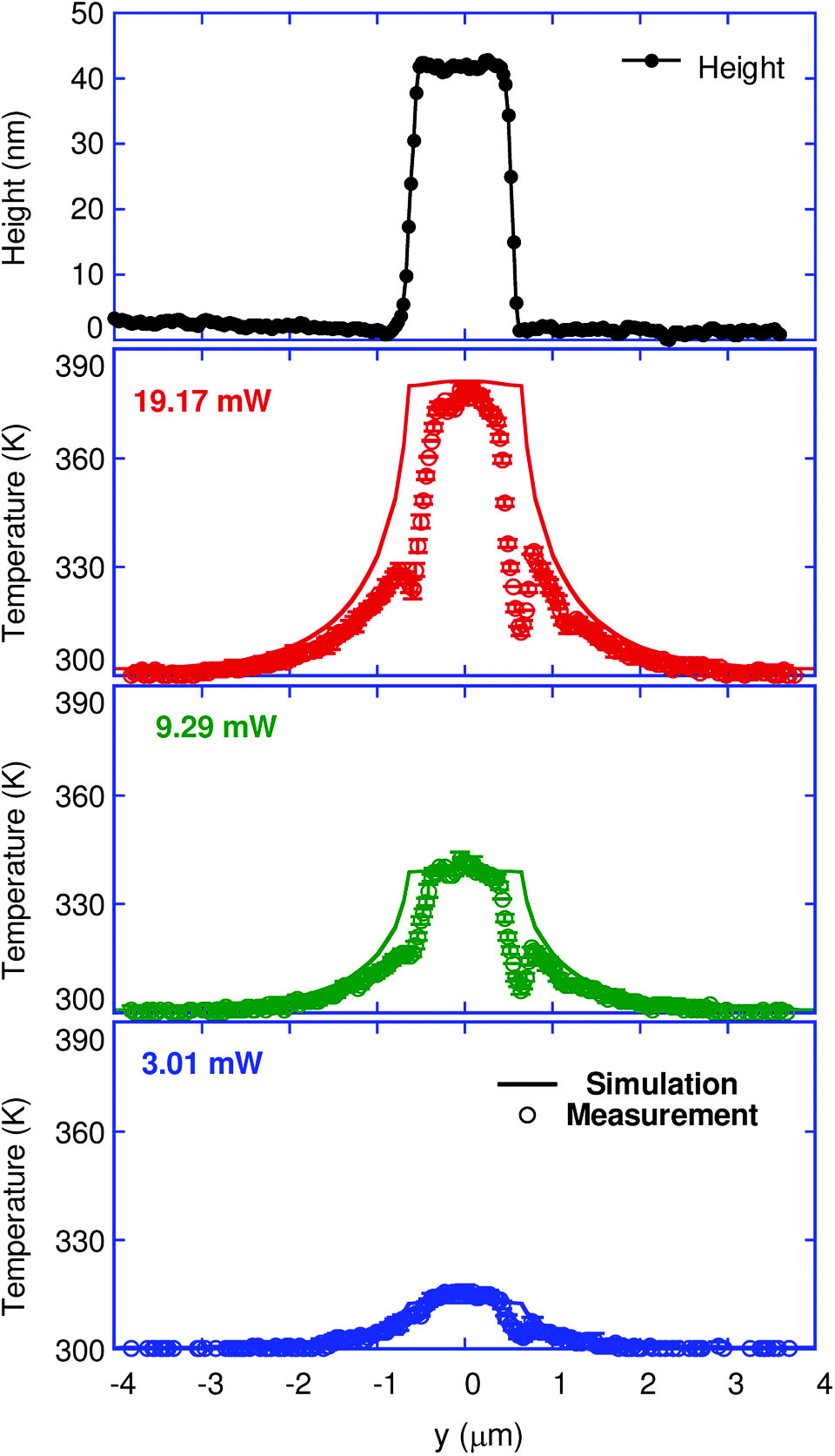 | ||
| Fig. 3 Topography of the tungsten line heater and its quantitative temperature profile obtained with the AFM-TR technique. Temperature profiles measured with the AFM-TR technique across the tungsten line heater when applying various amounts of input power (denoted by the symbols). Each profile represents the average data from three different measurements. The ANSYS simulation results (denoted by the solid line) are also plotted for comparison. The scan speed was 48 μm s−1, the scan step was 30 nm and the total number of measuring points was 256 per scan. | ||
Finally, the quantitative results obtained with the AFM-TR technique are compared with the results obtained with a commercially available SThM probe (NP SThM 02, TSP Nanoscopy). To demonstrate the potential of the technique for a versatile range of applications, we fabricated a new heater with Pt, as shown in Fig. 4. To induce substantial changes in the temperature distribution, the cross-sectional area of the Pt heater is changed abruptly. The line width of the heater on the left side is 422 nm while that on the right side is 2000 nm. The measured height of the heater is uniform and was found to be 72 nm. This heater is also patterned on 1 μm of SiO2 thermally grown on a Si substrate. The abrupt change in the line width of the heater generates the temperature gradient, and the local temperatures are measured at several selected points marked as A–F in Fig. 4a. When using the SThM probe, a pre-amplifier and a signal access module are necessary to determine the thermoelectric voltage signal and a topography image simultaneously. The SThM probe is calibrated identically to how the AFM Si probe is calibrated, except that the relationship between the thermoelectric voltage signal and the sample temperature is obtained rather than the relationship between ΔQPDR and the sample temperature. The results obtained with the both AFM-TR and SThM techniques while increasing the Joule heating power are plotted in Fig. 4b. It is clearly shown that both methods measure nearly identical temperatures for every point. As expected, the maximum temperature is obtained at point A and the temperature decreases as the distance from point A increases. The maximum error between the results obtained with both methods was found to be only 4.3 K at 387 K (i.e., 1.1%). This is a quite compelling result because the proposed AFM-TR technique does not require a specially fabricated probe or an additional complex signal processing system as the SThM technique does. It is confirmed here that the AFM-TR technique is a reliable form of thermometry despite the fact that it is a low-cost and readily accessible technique.
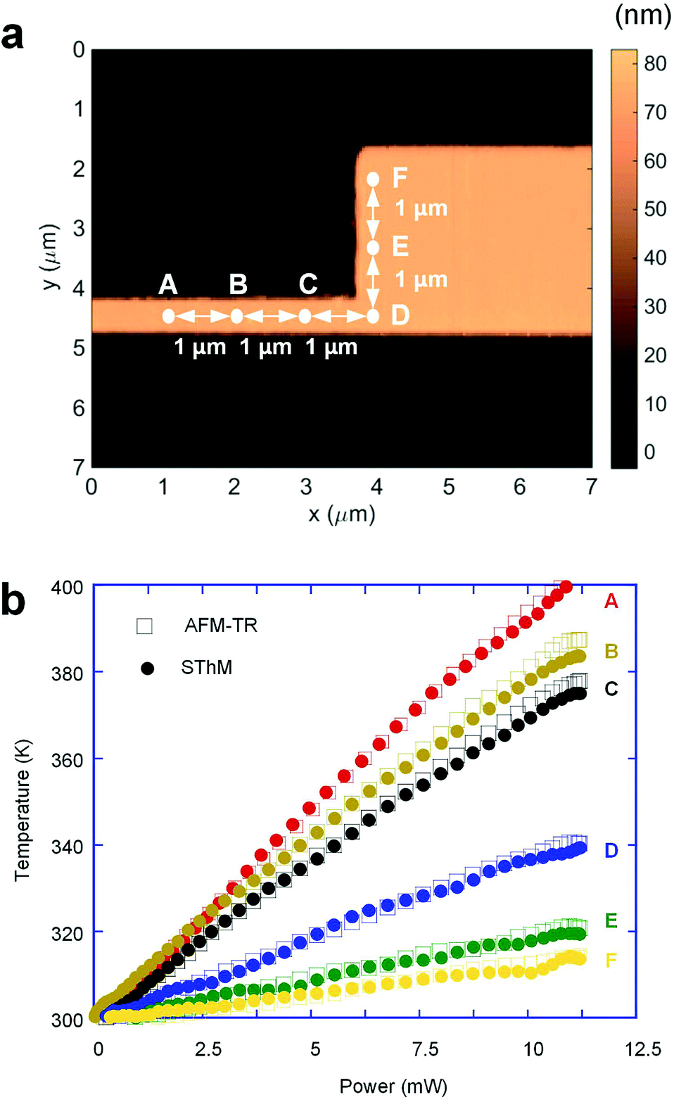 | ||
| Fig. 4 Validity of the proposed AFM-TR technique. (a) A topography image of the Pt heater sample. The locations of temperature-measurement points (i.e., A–F) are also noted. (b) Temperature variation measured with two techniques (AFM-TR and SThM) at each point under various input power levels. | ||
2.3 Discussion
Here, we describe the temperature resolution of the proposed technique. The measured standard deviation of ΔQPDR when there is no input power is 0.0067% (see Fig. 2b). With sensitivity of 0.013%/K as obtained through a calibration process, ΔTnoise can be estimated to be 0.52 K. This can be considered as the noise-limited temperature resolution of the proposed technique. Given that the temperature noise of the SThM probe without modulation and a noise filter is reportedly ∼10 K,13 our technique can produce results similar to those of SThM, as is apparent in Fig. 4b. The contact diameter can be calculated from classical Hertzian theory.1,23 The contact force of the Si probe was measured and found to be 67 nN during the temperature measurement using the AFM-TR technique. The diameter of the contact (i.e., aHertz) can be derived using the following relationship,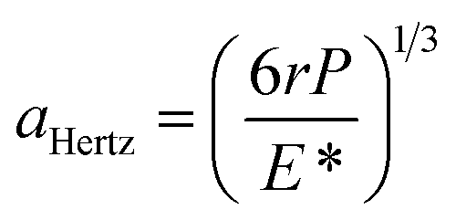 , where r (<20 nm for bare Si probes) is the tip radius, P is the contact force, and E* = [(1 − ν21)/E1 + (1 − ν22)/E2]−1 is the effective elastic modulus with ν being the Poisson's ratio and E being the modulus of elasticity.1,23 The subscripts 1 and 2 represent the two materials of the probe (Si) and the sample (W). The calculated diameter of the contact is less than 4.4 nm. The calculated contact diameter is similar to that of the SThM probe with a bare Si tip reported as ∼10 nm.13 Given that the bare AFM Si tip has a smaller radius (<20 nm) than the metal-coated SThM probe tip (20–50 nm),23,24 the contact diameter when using our technique would be smaller than that of the metal-coated SThM (i.e., 10–20 nm).23,24 The spatial resolution (Δx) can also be estimated from the noise in the temperature measurement and the maximum temperature gradient of the sample:2 Δx = ΔTnoise/(dT/dx). In Fig. 3, the maximum temperature gradient is measured and determined to be 0.322 K nm−1. Considering temperature noise of 0.52 K, the maximum spatial resolution can be estimated as 1.6 nm. Further, it should be noted that the measured temperature is in good agreement with the predicted data and distinguishable where neighboring points are separated by 30 nm, as in Fig. 3. All things considered, the actual resolution of our technique is expected to be 10–30 nm. Thus, it becomes obvious that quantitative thermometry with a sub-100 nm spatial resolution is possible with the AFM-TR technique.
Although the proposed AFM-TR technique is shown to produce results similar to those of SThM for simple measurements (i.e., Fig. 4), the SThM method has been developed for more precise temperature measurements, that is, removing edge effects (see Fig. 3) caused by a change in the contact area between a tip and a sample14,24,45 or nullifying the heat flux between a tip and a sample to measure the ‘actual’ temperature not perturbed by the measurement itself.24,45 These methodologies can also be applied to our AFM-TR technique if a heated AFM cantilever is used instead. Compared to previously reported SThM approaches with high sensitivity, our technique has an inherent limitation with regard to sensitivity; that is, the cantilever temperature is measured for our technique, whereas the probe tip temperature is measured for the SThM measurement. The temperature sensitivity can be defined by the thermal resistance of the heat path from the sample to the cantilever. For SThM using a thermocouple junction,23 the temperature sensitivity is determined via (Rtip + Rcan)/(Rts + Rtip + Rcan), where Rtip and Rcan are the thermal resistance of the probe tip and the cantilever, respectively, and Rts is the contact thermal resistance between the tip and the sample. According to Kim et al.,23 Rtip + Rcan is ∼5 × 10⁶ K W−1 and Rts is estimated to be 2 × 10⁸ K W−1 (SiO2–SiO2 contact) such that the reported sensitivity is ∼0.02 K K−1. However, for the proposed technique where the cantilever temperature is used, the temperature sensitivity can be defined as Rcan/(Rts + Rtip + Rcan). For a Si probe, Rcan is reportedly 2 × 10⁵ K W−1 and Rts is (1–2) × 108 K W−1 (Si–Si contact).13 In this case, the calculated temperature sensitivity of the Si probe for the AFM-TR technique is approximately 0.001 K K−1. This inherent limitation in the sensitivity arising from the geometry of the device can be overcome if a heated cantilever with a high Rcan value is introduced. Further, because the TR sensitivity is highly dependent on the cantilever thickness,40 a heated cantilever with an optimized thickness is expected to increase the sensitivity of the proposed technique. The reported SThM shows a much higher temperature resolution (i.e., 7 mK)14 than that by our technique (i.e., 520 mK). Such a low temperature resolution can be mitigated by modulation, reducing the electrical noise in the QPD signal. In fact, steady-state measurements with SThM show relatively large amounts of temperature noise (i.e., ∼10 K 13), though these are later reduced dramatically to 7 mK with modulation.14
3 Conclusions
In summary, we proposed a versatile AFM-based thermometry with a sub-100 nm spatial resolution. The temperature profile can be obtained only with a conventional AFM setup and conventional AFM probe by exploiting the TR characteristic of the conventional AFM Si probe. The laser diode and the QPD, originally used for topography imaging, can also be employed to detect changes in the laser signal which is altered by the temperature of the sample. Through calibration, the quantitative temperature measurements at resolutions down to 30 nm can be achieved. The temperature measured with the present method shows excellent agreement with the temperature distribution predicted by a simulation and the temperature measured with a commercially available SThM probe, demonstrating the validity of the AFM-TR technique as a reliable form of thermometry. Without using fragile and expensive probes and a complex signal processing system, this technique provides a means by which to measure the temperature only with the conventional AFM setup. It should be noted that this is a wholly new concept and that this work is the very first to concentrate on this technique. Given that there are much room left with regard to this technique to realize improved performance or for to apply it in various areas, future studies are expected. The proposed readily accessible nanoscale thermometry is suitable for researchers from various fields and thus will promote our understanding of diverse nanoscale thermal transport phenomena in various environments.Conflicts of interest
There are no conflicts to declare.Acknowledgements
This research was supported by Basic Science Research Program through the National Research Foundation of Korea (NRF) funded by the Ministry of Science and ICT (NRF-2017R1A2B2011192 and NRF-2015R1A2A1A10055060).References
- A. Majumdar, Annu. Rev. Mater. Sci., 1999, 29, 505–585 CrossRef.
- D. G. Cahill, K. Goodson and A. Majumdar, J. Heat Transfer, 2002, 124, 223–241 CrossRef.
- J. Christofferson, K. Maize, Y. Ezzahri, J. Shabani, X. Wang and A. Shakouri, J. Electron. Packag., 2008, 130, 041101 CrossRef.
- C. D. S. Brites, P. P. Lima, N. J. O. Silva, A. Millán, V. S. Amaral, F. Palacio and L. D. Carlos, Nanoscale, 2012, 4, 4799–4829 RSC.
- D. G. Cahill, P. V. Braun, G. Chen, D. R. Clarke, S. Fan, K. E. Goodson, P. Keblinski, W. P. King, G. D. Mahan, A. Majumdar, H. J. Maris, S. R. Phillpot, E. Pop and L. Shi, Appl. Phys. Rev., 2014, 1, 011305 Search PubMed.
- S. Gomès, A. Assy and P.-O. Chapuis, Phys. Status Solidi A, 2015, 212, 477–494 CrossRef.
- M. J. Pereira, J. S. Amaral, N. J. O. Silva and V. S. Amaral, Microsc. Microanal., 2016, 22, 1270–1280 CrossRef PubMed.
- P. Kolodner and J. A. Tyson, Appl. Phys. Lett., 1983, 42, 117–119 CrossRef.
- L. Aigouy, G. Tessier, M. Mortier and B. Charlot, Appl. Phys. Lett., 2005, 87, 184105 CrossRef.
- G.-Y. Zhuo, H.-C. Su, H.-Y. Wang and M.-C. Chan, Opt. Express, 2017, 25, 21548–21558 CrossRef PubMed.
- D. Halbertal, J. Cuppens, M. B. Shalom, L. Embon, N. Shadmi, Y. Anahory, H. R. Naren, J. Sarkar, A. Uri, Y. Ronen, Y. Myasoedov, L. S. Levitov, E. Joselevich, A. K. Geim and E. Zeldov, Nature, 2016, 539, 407–410 CrossRef PubMed.
- K. Park, G. Hwang, H. Kim, J. Kim, W. Kim, S. Kim and O. Kwon, Appl. Phys. Lett., 2016, 108, 071907 CrossRef.
- F. Menges, H. Riel, A. Stemmer and B. Gotsmann, Nano Lett., 2012, 12, 596–601 CrossRef PubMed.
- F. Menges, P. Mensch, H. Schmid, H. Riel, A. Stemmer and B. Gotsmann, Nat. Commun., 2016, 7, 10874 CrossRef PubMed.
- M. Mecklenburg, W. A. Hubbard, E. R. White, R. Dhall, S. B. Cronin, S. Aloni and B. C. Regan, Science, 2015, 347, 629–632 CrossRef PubMed.
- E. Yalon, S. Deshmukh, M. M. Rojo, F. Lian, C. M. Neumann, F. Xiong and E. Pop, Sci. Rep., 2017, 7, 15360 CrossRef PubMed.
- O. Semenov, A. Vassighi and M. Sachdev, IEEE Trans. Device Mater. Reliab., 2006, 6, 17–27 CrossRef.
- L. Shi, O. Kwon, A. C. Miner and A. Majumdar, J. Microelectromech. Syst., 2001, 10, 370–378 CrossRef.
- L. Shi and A. Majumdar, J. Heat Transfer, 2002, 124, 329–337 CrossRef.
- G. Wielgoszewski, P. Sulecki, T. Gotszalk, P. Janus, D. Szmigiel, P. Grabiec and E. Zschech, J. Vac. Sci. Technol., B: Nanotechnol. Microelectron.: Mater., Process., Meas., Phenom., 2010, 28, C6N7–C6N11 Search PubMed.
- G. Wielgoszewski, P. Sulecki, P. Janus, P. Grabiec, E. Zschech and T. Gotszalk, Meas. Sci. Technol., 2011, 22, 094023 CrossRef.
- K. Kim, J. Chung, G. Hwang, O. Kwon and J. S. Lee, ACS Nano, 2011, 5, 8700–8709 CrossRef PubMed.
- K. Kim, W. Jeong, W. Lee and P. Reddy, ACS Nano, 2012, 6, 4248–4257 CrossRef PubMed.
- G. Hwang, J. Chung and O. Kwon, Rev. Sci. Instrum., 2014, 85, 114901 CrossRef PubMed.
- S. Sadat, A. Tan, Y. J. Chua and P. Reddy, Nano Lett., 2010, 10, 2613–2617 CrossRef PubMed.
- K. L. Grosse, E. Pop and W. P. King, J. Appl. Phys., 2014, 116, 124508 CrossRef.
- K. L. Grosse, M.-H. Bae, F. Lian, E. Pop and W. P. King, Nat. Nanotechnol., 2011, 6, 287–290 CrossRef PubMed.
- S. P. Gurrum, W. P. King, Y. K. Joshi and K. Ramakrishna, J. Heat Transfer, 2008, 130, 082403 CrossRef.
- A. Soudi, R. D. Dawson and Y. Gu, ACS Nano, 2011, 5, 255–262 CrossRef PubMed.
- F. Menges, H. Riel, A. Stemmer, C. Dimitrakopoulos and B. Gotsmann, Phys. Rev. Lett., 2013, 111, 205901 CrossRef PubMed.
- W. Jeong, K. Kim, Y. Kim, W. Lee and P. Reddy, Sci. Rep., 2014, 4, 4975 CrossRef.
- K. Yoon, G. Hwang, J. Chung, H. G. Kim, O. Kwon, K. D. Kihm and J. S. Lee, Carbon, 2014, 76, 77–83 CrossRef.
- G. Hwang and O. Kwon, Int. J. Therm. Sci., 2016, 108, 81–88 CrossRef.
- G. Hwang and O. Kwon, Nanoscale, 2016, 8, 5280–5290 RSC.
- J. S. Reparaz, E. Chavez-Angel, M. R. Wagner, B. Graczykowski, J. Gomis-Bresco, F. Alzina and C. M. Sotomayor Torres, Rev. Sci. Instrum., 2014, 85, 034901 CrossRef PubMed.
- L. R. de Freitas, E. C. da Silva, A. M. Mansanares, G. Tessier and D. Fournier, J. Appl. Phys., 2005, 98, 063508 CrossRef.
- G. Tessier, M.-L. Polignano, S. Pavageau, C. Filloy, D. Fournier, F. Cerutti and I. Mica, J. Phys. D: Appl. Phys., 2006, 39, 4159 CrossRef.
- W. J. Choi, S. Y. Ryu, J. K. Kim, D. U. Kim, G. H. Kim and K. S. Chang, Opt. Lett., 2013, 38, 3581–3584 CrossRef PubMed.
- H. Park, B. J. Lee and J. Lee, Rev. Sci. Instrum., 2014, 85, 036109 CrossRef PubMed.
- J. Rho and B. J. Lee, J. Heat Transfer, 2017, 139, 052703 CrossRef.
- K. E. Goodson and M. Asheghi, Microscale Thermophys. Eng., 1997, 1, 225–235 CrossRef.
- S. Gomés, P.-O. Chapuis, F. Nepveu, N. Trannoy, S. Volz, B. Charlot, G. Tessier, S. Dilhaire, B. Cretin and P. Vairac, IEEE Trans. Compon. Packag. Technol., 2007, 30, 424–431 Search PubMed.
- K. Kim, J. Chung, J. Won, O. Kwon, J. S. Lee, S. H. Park and Y. K. Choi, Appl. Phys. Lett., 2008, 93, 203115 CrossRef.
- J. Chung, K. Kim, G. Hwang, O. Kwon, S. Jung, J. Lee, J. W. Lee and G. T. Kim, Rev. Sci. Instrum., 2010, 81, 114901 CrossRef PubMed.
- J. Chung, K. Kim, G. Hwang, O. Kwon, Y. K. Choi and J. S. Lee, Int. J. Therm. Sci., 2012, 62, 109–113 CrossRef.
- J. Martinek, P. Klapetek and A. C. Campbell, Ultramicroscopy, 2015, 155, 55–61 CrossRef PubMed.
- E. Saïdi, B. Samson, L. Aigouy, S. Volz, P. Löw, C. Bergaud and M. Mortier, Nanotechnology, 2009, 20, 115703 CrossRef PubMed.
- S. Gomès, N. Trannoy and P. Grossel, Meas. Sci. Technol., 1999, 10, 805–811 CrossRef.
Footnotes |
| † Electronic supplementary information (ESI) available. See DOI: 10.1039/c8ra05937c |
| ‡ These authors contributed equally to this work. |
| This journal is © The Royal Society of Chemistry 2018 |