
 Open Access Article
 This Open Access Article is licensed under a Creative Commons Attribution-Non Commercial 3.0 Unported Licence
Characterization of the piezoresistance in highly doped p-type 3C-SiC at cryogenic temperatures†
Hoang-Phuong Phan *ab,
Karen M. Dowlingb,
Tuan-Khoa Nguyena,
Caitlin A. Chapinb,
Toan Dinha,
Ruth A. Millerb,
Jisheng Hana,
Alan Iacopia,
Debbie G. Seneskybc,
Dzung Viet Daoad and
Nam-Trung Nguyena
*ab,
Karen M. Dowlingb,
Tuan-Khoa Nguyena,
Caitlin A. Chapinb,
Toan Dinha,
Ruth A. Millerb,
Jisheng Hana,
Alan Iacopia,
Debbie G. Seneskybc,
Dzung Viet Daoad and
Nam-Trung Nguyena
aQueensland Micro-Nanotechnology Centre, Griffith University, Queensland, Australia. E-mail: hoangphuong.phan@griffithuni.edu.au
bDepartment of Aeronautics and Astronautic, Stanford University, USA
cDepartment of Electrical Engineering, Stanford University, CA, USA
dSchool of Engineering, Griffith University, Queensland, Australia
First published on 24th August 2018
Abstract
This paper reports on the piezoresistive effect in p-type 3C-SiC thin film mechanical sensing at cryogenic conditions. Nanothin 3C-SiC films with a carrier concentration of 2 × 1019 cm−3 were epitaxially grown on a Si substrate using the LPCVD process, followed by photolithography and UV laser engraving processes to form SiC-on-Si pressure sensors. The magnitude of the piezoresistive effect was measured by monitoring the change of the SiC conductance subjected to pressurizing/depressurizing cycles at different temperatures. Experimental results showed a relatively stable piezoresistive effect in the highly doped 3C-SiC film with the gauge factor slightly increased by 20% at 150 K with respect to that at room temperature. The data was also in good agreement with theoretical analysis obtained based on the charge transfer phenomenon. This finding demonstrates the potential of 3C-SiC for MEMS sensors used in a large range of temperatures from cryogenic to high temperatures.
Introduction
Wide band gap semiconductors such as gallium nitride (GaN), silicon carbide (SiC), and diamond like carbon (DLC) have been of significant interest for harsh environment applications.1–6 Among these materials, SiC has proved to be an outstanding candidate owing to its chemical inertness, availability of materials, as well as well-established fabrication technology including the capability of growing on a Si substrate. Numerous SiC based Micro Electro Mechanical Systems (MEMS) sensors have been developed, including UV sensors, gas sensors, and mechanical sensors.7–12 For structural health monitoring systems, the use of mechanical sensors is imperative; for example, strain sensors can detect crack generation, while pressure sensors can be employed for the feedback control of an engine to enhance its fuel efficiency. A large number of studies have been carried out to investigate the piezoresistance in SiC for mechanical sensing applications. With the capability of tuning the energy bands under strain, SiC exhibits a relatively high gauge factor ranging from 10 to 50.13–16 Along with the large Young's modulus and excellent mechanical strength, the piezoresistive effect in SiC has been utilized in applications requiring fast response and extreme mechanical loads such as high-shock sensors and high-g accelerometers.17 Additionally, piezoresistive SiC pressure sensors which can operate at high temperatures have also been demonstrated.18,19 For instance, Okojie et al. developed 4H-SiC pressure sensors which can function up to 1000 K.20 Although numerous studies have been conducted on SiC at high temperatures, the piezoresistance of the material at negative temperatures has rarely been reported. As low temperature tolerance is imperative in several fields (e.g. space exploration where temperatures can be below 100 K),21,22 investigation into the feasibility of SiC for low temperature applications is significant.This work reports for the first time the piezoresistance of p-type 3C-SiC at low temperatures down to 150 K. Our experimental results show that the gauge factor of p-type 3C-SiC films slightly increased with decreasing temperature, which is in good agreement with theoretical analysis.
Results and discussion
The growth process of the SiC film can be found elsewhere,23 in which low pressure chemical vapor deposition was utilized to epitaxially deposit SiC on a 6-inch Si wafer (p-type with a carrier concentration of 1014 cm−3). The crystal quality and surface roughness of the SiC films were reported in our previous studies.24 The SiC films were found to be p-type semiconductor with the carrier concentration found to be approximately 2 × 1019 cm−3 using Hall-measurement and/or hot probe technique. Following the SiC deposition process, lithography and inductive coupled plasma etching were employed to form SiC micro resistors with dimension of 550 μm × 50 μm × 380 nm. Subsequently, aluminum was deposited and patterned to form the electrodes for the SiC resistors. Finally, UV laser engraving was utilized to form SiC on Si diaphragm with dimensions of 7 mm × 7 mm × 150 μm. UV laser engraving was chosen due to the high etching rate of 16 μm min−1 in comparison to other dry etching methods with etching rates of typically below 10 μm min−1. This high etching rate allows quick prototyping of pressure sensors.25 In addition, the use of laser engraving eliminates the requirement for the hard-mask used in backside-Si-etching, which significantly simplifies our fabrication process (see the ESI†). Subsequently, the as-fabricated pressure sensor was mounted on a home-built PCB board to form an enclosed chamber under the SiC/Si membrane. Fig. 1(a) and (b) show photographs of the SiC/Si pressure sensor.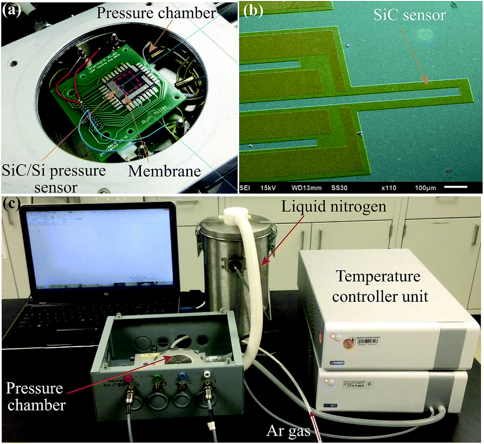 | ||
| Fig. 1 Photographs of fabricated device and the experimental setup. (a) SiC on Si pressure sensor mounted on a PCB board; (b) SEM image of a SiC resistor (false colored); (c) experimental setup for characterization of the piezoresistive effect in 3C-SiC at cryogenic temperature. | ||
Initially, the piezoresistive effect of the SiC film was characterized at room temperature using the experimental setup shown in Fig. 1(c) where the PCB boards were placed on a heating/cooling chuck. A thin layer of thermal grease was applied between the surface of the PCB and the chuck to enhance the thermal conductivity. The Linkam™ chamber was then filled with Ar gas to apply pressure to the sensor. The applied pressure was controlled using a pressure regulator with a manual incrementation of approximately 0.25 bar per step. Further detail of the experimental setup and its schematic sketch are presented in the ESI.† The applied voltage at the SiC resistor was then fixed at 0.5 V, and the current was monitored and recorded using an Agilent™ Semiconductor Device Analyzer B1500 while increasing the gas pressure. It is evident from Fig. 2(a) that the current decreased with increasing pressure from 0 to 2.1 bar, indicating a positive gauge factor in the p-type 3C-SiC. The current also returned to its initial value when the applied pressure was completely released. Additionally, the variation in the current due to the applied pressure at room temperature shows excellent repeatability after several pressurizing/depressurizing cycles, as illustrated in Fig. 2(b).
 | ||
| Fig. 2 Piezoresistive effect in p-type 3C-SiC at room temperature. (a) The output current under increasing applied pressure; (b) the good repeatability of the pressure sensors under several testing cycles; (c) the linear relationship between the resistance change and applied pressure. | ||
Fig. 2(c) plots the resistance change of the SiC resistor against applied pressure, showing a good linearity which is preferable for mechanical sensing applications. The strain induced into the SiC resistors was estimated based on finite element analysis (FEA) using COMSOL Multiphysics™. It should be pointed out that since the thickness of the Si substrate was significantly larger than that of the Si membrane, the strain applied to the SiC piezoresistor was almost the same as that of the top surface of the Si membrane. Additionally, since the SiC resistor was located at the center of the edge of the SiC/Si membrane, the shear and transverse strains were approximately two orders of magnitude smaller than that of longitudinal strain, Fig. 2(c) inset. Therefore, only the longitudinal gauge factor significantly contributed to the response of the SiC resistors under applied pressure, while the influence of shear and transverse gauge factors was negligible. Based on the simulation results, the longitudinal strain applied to the SiC resistor under a pressure of 2 bar was found to be approximately 600 ppm. Consequently, the longitudinal gauge factor (GFl = (ΔR/R)/ε) of the 3C-SiC resistors were found to be 30. This result was consistent with our previously reported results, measured using the bending beam method.16
The temperature of the device was then reduced using liquid nitrogen. The temperature of SiC/Si chip was estimated by the set-temperature of the thermal chuck after a calibration test relating the chuck temperature to the temperature reported by a commercial thermocouple epoxied to the surface was completed. The I–V curve of the resistance at 150 K shows good ohmic contact between Al and p-type SiC was maintained at low temperatures. Furthermore, the current leakage to the substrate at low temperatures was significantly lower than the current passing through the SiC resistors as plotted in Fig. 3(a). This is due to the discontinuity between the valance bands of SiC and Si as well as the reduction of the charge carriers in Si substrate, resulting in less hole tunneling through the potential barrier between SiC and Si at low temperature. It should also be noted that, the designed SiC resistors possess four electrode pads, enabling four-terminal measurement. However, since the contact resistance was significantly smaller than that of the SiC resistor, the two-terminal measurement was applied to monitor the change of SiC resistance under applied pressure.
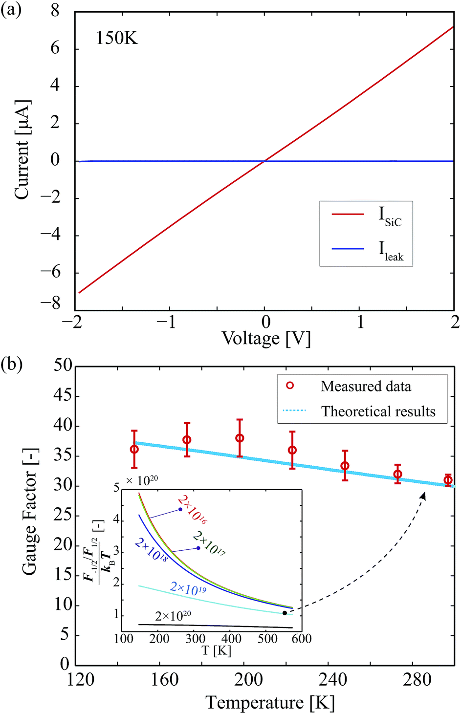 | ||
Fig. 3 Piezoresistive effect in p-type 3C-SiC at cryogenic temperature. (a) Good ohmic contact and small current leakage were maintained at low temperatures. (b) The gauge factor of SiC at room temperature down to 150 K. Inset: estimation of the Fermi–Dirac integral  in a wide range of temperatures at different carrier concentration (unit: cm−3). in a wide range of temperatures at different carrier concentration (unit: cm−3). | ||
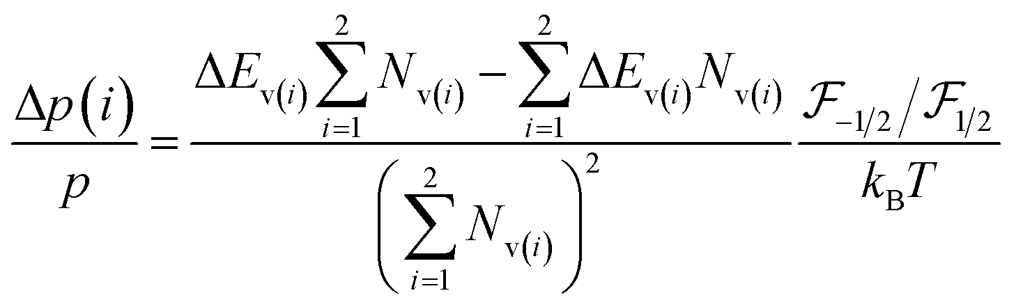
The piezoresistive effect of the SiC pressure sensors at cryogenic temperature was then investigated by pressurizing the chamber using Ar gas as described above. The gauge factor of the SiC films at low temperature was calculated in which the change in the stiffness of Si membrane with temperature was taken into account (ΔESi(T) = ESi × ΔT × γ, where γ = −50 ppm K−1 is the temperature coefficient of Young's modulus).26 Fig. 3(c) shows the relationship between the gauge factors and temperature. It is evident that, there was a small change in the piezoresistive effect in the p-type 3C-SiC at low temperature; the gauge factor increased from 30 at 300 K to 36 at 150 K. The piezoresistive effect in p-type semiconductors is caused by the splitting of heavy hole and light hole bands when the materials are subjected to a mechanical strain. Under the deformation of the energy structures, the holes will re-populate between these two bands, following the Boltzmann distribution:27
 | (1) |
 is the Fermi–Dirac integral, respectively. Assuming that the total number of holes in highly doped semiconductors remains constant under applied strain
  ,28 the changing rate of the charge carrier in the heavy and light hole bands is given by:27
 | (2) |
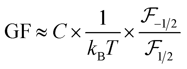
Since the change in the electrical conductance is propositional to the modification of the hole concentration, the gauge factor of p-type semiconductor can be simplified as:29
 | (3) |
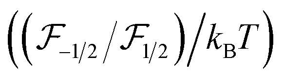 depends not only on temperature but also on the carrier concentration. This component was calculated using the Chang–Izabelle30 approximating method and plotted in the inset of Fig. 3. The analytical result show that
  was higher at low carrier concentrations, exhibiting the same trend as experimental data reported in the literature.31 It also evident that the ratio of the Fermi–Dirac integral to kBT was relatively stable for high carrier concentration, but changes markedly with temperature for low doped SiC. This result was consistent with our experimental data plotted in Fig. 3(b) showing the stability of the piezoresistive effect in p-type 3C-SiC at temperatures down to 150 K.
Conclusion
This work investigated the piezoresistive effect in highly doped p-type 3C-SiC grown on a Si substrate in cryogenic temperatures. A large and temperature-stable gauge factor of above 30 was found in the p-type 3C-SiC. The stability and the high sensitivity of the piezoresistive effect demonstrate the potential of p-type 3C-SiC for mechanical sensing at cryogenic temperatures.Conflicts of interest
There are no conflicts to declare.Acknowledgements
This work was partially funded by the linkage grants LP150100153 and LP160101553 from the Australian Research Council (ARC). This work was performed in part at the Queensland node of the Australian National Fabrication Facility, a company established under the National Collaborative Research Infrastructure Strategy to provide nano and micro-fabrication facilities for Australia's researchers. H.-P. Phan acknowledges research grants from the Australian Nanotechnology Network Overseas Travel Fellowship and the Griffith University New Researcher Grant.References
- D. G. Senesky, B. Jamshidi, K. B. Cheng and A. P. Pisano, IEEE Sens. J., 2009, 9, 1472–1478 Search PubMed.
- A. Qamar, P. Tanner, D. V. Dao, H. P. Phan and T. Dinh, IEEE Electron Device Lett., 2014, 35(12), 1293–1295 Search PubMed.
- F. Gao, J. Zheng, M. Wang, G. Wei and W. Yang, Chem. Commun., 2011, 47(43), 11993–11995 RSC.
- A. L. Vikharev, A. M. Gorbachev, M. A. Lobaev, A. B. Muchnikov, D. B. Radishev, V. A. Isaev, V. V. Chernov, S. A. Bogdanov, M. N. Drozdov and J. E. Butler, Phys. Status Solidi RRL, 2016, 10(4), 324–327 CrossRef.
- T. Chen, Y. Huang, D. Yang, R. Carius and F. Finger, Phys. Status Solidi RRL, 2010, 4(34), 61–63 CrossRef.
- H. P. Phan, H. H. Cheng, T. Dinh, B. Wood and T. K. Nguyen, et al., ACS Appl. Mater. Interfaces, 2017, 9(33), 27365–27371 CrossRef PubMed.
- M. Massimo, P. Shukla, R. Mallik, M. Kumar, R. Previti, G. D. Marco, A. Sciuto, R. A. Puglisi and V. Raineri, IEEE Sens. J., 2011, 11(2), 377–381 Search PubMed.
- K.-S. Kim and G.-S. Chung, Sens. Actuators, B, 2011, 160(1), 1232–1236 CrossRef.
- H. P. Phan, T. Dinh, T. Kozeki, T. K. Nguyen, A. Qamar, T. Namazu, N. T. Nguyen and D. V. Dao, Appl. Phys. Lett., 2016, 109(12), 123502 CrossRef.
- T. Dinh, H. P. Phan, A. Qamar, P. Woodfield, N. T. Nguyen and D. V. Dao, J. Microelectromech. Syst., 2017, 26(5), 966–986 Search PubMed.
- J. Bi, G. Wei, L. Wang, F. Gao, J. Zheng, B. Tang and W. Yang, J. Mater. Chem. C, 2013, 1(30), 4514–4517 RSC.
- X. Li, S. Chen, P. Ying, F. Gao, Q. Liu, M. Shang and W. Yang, J. Mater. Chem. C, 2016, 4(27), 6466–6472 RSC.
- T. K. Nguyen, H. P. Phan, T. Dinh, J. Han, S. Dimitrijev, P. Tanner, A. R. M. Foisal, Y. Zhu, N. T. Nguyen and D. V. Dao, Electron Device Lett., 2017, 38(7), 955–958 Search PubMed.
- M. A. Fraga, H. Furlan, R. S. Pessoa, L. A. Rasia and C. F. R. Mateus, Microsyst. Technol., 2012, 18(7–8), 1027–1033 CrossRef.
- R. Shao, K. Zheng, Y. Zhang, Y. Li, Z. Zhang and X. Han, Appl. Phys. Lett., 2012, 101(23), 233109 CrossRef.
- H. P. Phan, T. Dinh, T. Kozeki, T. K. Nguyen, A. Qamar, T. Namazu, N. T. Nguyen and D. V. Dao, Electron Device Lett., 2016, 37(8), 1029–1032 Search PubMed.
- A. R. Atwell, R. S. Okojie, K. T. Kornegay, S. L. Roberson and A. Beliveau, Sens. Actuators, A, 2003, 104(1), 11–18 CrossRef.
- R. S. Okojie, C. Blaha, D. Lukco, V. Nguyen and E. Savrun, 2010 IEEE Sensors Conf., 2010, pp. 2269–2274 Search PubMed.
- C. H. Wu, C. A. Zorman and M. Mehregany, IEEE Sens. J., 2006, 6(2), 316–324 CrossRef.
- R. S. Okojie, D. Lukco, V. Nguyen and E. Savrun, Electron Device Lett., 2015, 36(2), 174–176 Search PubMed.
- H. So and D. G. Senesky, IEEE Sens. J., 2017, 17(15), 4752–4756 Search PubMed.
- S. J. Zhang, F. Li and F. P. Yu, in Structural Health Monitoring (SHM) in Aerospace Structures, 2016, pp. 59–93 Search PubMed.
- L. Wang, S. Dimitrijev and J. Han, et al., J. Cryst. Growth, 2011, 329, 67–70 CrossRef.
- A. Qamar, H. P. Phan, J. Han, P. Tanner, T. Dinh, L. Wang, S. Dimitrijev and D. V. Dao, J. Mater. Chem. C, 2015, 3(34), 8804–8809 RSC.
- K. M. Dowling, H. So, A. Toor, C. A. Chapin and D. G. Senesky, Microelectron. Eng., 2017, 173, 54–57 CrossRef.
- E. J. Boyd, L. Li, R. Blue and D. Uttamchandani, Sens. Actuators, A, 2013, 198, 75–80 CrossRef.
- T. Toriyama and S. Sugiyama, J. Microelectromech. Syst., 2002, 11(5), 598–604 CrossRef.
- Y. Sun, S. E. Thompson and T. Nishida, Strain effect in semiconductors: theory and device applications. Springer, 2009 Search PubMed.
- H. P. Phan, D. V. Dao, K. Nakamura, S. Dimitrijev and N. T. Nguyen, J. Microelectromech. Syst., 2015, 24(6), 1663–1677 Search PubMed.
- T. Y. Chang and A. Izabelle, J. Appl. Phys., 1989, 65(5), 2162–2164 CrossRef.
- M. Eickhoff, M. Moller and G. Kroetz, et al., J. Appl. Phys., 2004, 96, 2872–2879 CrossRef.
Footnote |
| † Electronic supplementary information (ESI) available. See DOI: 10.1039/c8ra05797d |
| This journal is © The Royal Society of Chemistry 2018 |