
 Open Access Article
 This Open Access Article is licensed under a Creative Commons Attribution-Non Commercial 3.0 Unported Licence
Electrical properties of O-self-doped boron-nitride nanotubes and the piezoelectric effects of their freestanding network film†
Chuncheng Ban a,
Ling Li*abc and
Liuxiao Weiabc
a,
Ling Li*abc and
Liuxiao Weiabc
aMEMS Center, Harbin Institute of Technology, Harbin, 150001, China. E-mail: linglimems@hit.edu.cn
bState Key Laboratory of Urban Water Resource & Environment (Harbin Institute of Technology), Harbin 150001, China
cKey Laboratory of Micro-systems and Micro-Structures Manufacturing, Ministry of Education, Harbin 150001, China
First published on 16th August 2018
Abstract
Boron-nitride nanotubes (BNNTs) are a common one-dimensional (1D) nanostructure that possess piezoelectric potential due to ion-covalent boron-nitride (BN) bonding. Harnessing the advantages offered by high-stability BN structures, these materials have been used for various new applications such as nanogenerators, nanotransistors, and nano-artificial eardrums. In this paper, we used nano-iron oxide red as a catalyst and boron powder in an aqueous dispersion as the boron source to synthesize high-purity O-self-doped BNNTs and film. We investigated the electrical properties of O-self-doped BNNTs and the piezoelectricity of freestanding BNNT film and demonstrated that the electrical properties of O-self-doped BNNTs improved dramatically compared to those of non-doped BNNTs. We also analyzed the band gaps and density of states (DOS) of the O-self-doped BNNTs with the Spanish Initiative for Electronic Simulation with Thousands of Atoms (SIESTA) code to explain the improvement. In addition, we revealed the piezoelectric voltage coefficient g31 of O-self-doped BNNTs (0.28 V m N−1) network films, which can guide future applications for vibration nanosensors and transducers under extreme conditions.
Introduction
1D nanostructures can be made of many types of NT materials, such as carbon NTs (CNTs), BNNTs, zinc oxide NTs, and titanium dioxide NTs. Wide band gap (5.6 eV) BNNTs have the same crystalline structure as carbon NTs.1,2 Compared to other 1D nanostructures, BNNTs exhibit high oxidation-thermal stability and chemical inertness.3 However, limited synthetic methods have encouraged some researchers to focus on the composite films inside BNNTs. These studies have revealed some promising properties, including linear piezoelectric and nonlinear electroactive strain, thermal, electrical, and mechanical properties of composite films.4–8 Furthermore, the piezoelectric potential distribution under an applied stress has been attributed to the noncentral symmetry of BNNTs.9 Currently, these unique properties of BNNTs are utilized in many applications, such as nanotransistors, nanosensors, nanogenerators and nanopiezoelectricity.10,11Although BNNTs possess many advantages beneficial for practical applications, some major obstacles prevent their piezoelectric application, including high impedance and purity and yield. Many researchers are searching for elements and methods that are more efficient for BNNT doping to decrease resistance, and many studies have focused on theoretical simulations based on the Kohn–Sham equations. For instance, some studies investigated Au-doped BNNTs, V-doped BNNTs and C-doped BNNTs.12–14 However, doping with larger atomic number elements has been challenging because these elements only adsorb on the NT surface. In addition, the purity and yield of C-doped BNNTs is limited. Motivated by these issues, O element doped BNNTs seems to be a better choice. Moreover, recently reports reveals O doped BN material process an excellent ferromagnetic properties at room temperature, and other attracting properties.15,16 So that, this properties suggest that O doped BNNT is likely to a very promising piezoelectric nanomaterial for a widely application.
In this paper, a high purity, high yield and stable O-self-doped BNNTs were synthesized by a nano-ferric oxide-catalyzed boron annealing method in this article. These BNNTs were assembled into a freestanding film via vacuum filtration of a BNNT suspension, which is similar to the buckypaper of CNTs.17 We investigated the electrical properties of the O-self-doped BNNTs and their network film using thermionic-field emission theory. With further research, we determined that the band gap of the O-self-doped BNNTs decreased upon the introduction of a donor level in the BNNTs, which agreed with some calculations based on the density functional theory (DFT).18 In addition, we investigated for the first time the piezoelectric coefficient of the randomly oriented pure O-self-doped BNNT network film without any polymer. Using these factors and the relative dielectric constant, piezoelectric strain coefficient can be estimated.19
Experimental
Synthetic procedures
The O-doped BNNTs were synthetized using nano-iron oxide red as a catalyst at high temperature, and a schematic diagram of BNNT preparation system is shown. First, amorphous boron powder (ALDRICH, ≥95% amorphous boron power) and nano-sized Fe2O3 powder (Aladdin, 30 nm 99.5% Fe2O3) with a high surface area were mixed. Next, 0.2 g of the mixed powder was placed into vials filled with ammonia water in a glove box under N2 atmosphere to prepare the raw material for the synthesis process. After ultrasonicating the raw material for 10 min, the raw ink material was coated on a cleaned stainless-steel substrate. Finally, the stainless-steel substrate was placed into a tube furnace at 1150 °C, and the furnace was filled with N2 + 15% H2 to synthesize BNNTs.BNNT network film preparation method
The BNNTs were peeled from the stainless-steel substrate and still contained some impurities and the catalyst. The purity of NTs in the suspension greatly affected the quality of the BNNT network film and was key to successful preparation of the film. To increase the purity of the BNNTs, a wash and oxidation method with nitric acid at a high temperature was performed. We then used ultrasonic dispersion to obtain a uniformly dispersed BNNT suspension solution in ethyl alcohol with a concentration of 2.5 mg ml−1. The BNNT network film was fabricated using 20 ml of the suspension with microfiltration membrane paper. The polytetrafluoroethylene microfiltration membrane paper (PTFE) had a characteristic 0.22 μm pore size and was attached to a 13 mm Luer syringe filter. As the solvent evaporated under a low vacuum at room temperature, the local concentration of BNNTs near the membrane rapidly increased, and BNNTs were deposited on the microfiltration paper to form a paper-like network film as shown in Fig. S2 and S3.†First principles calculation
Calculations were performed using the SIESTA code, which is based on DFT.29 All the calculations were based on a first principles pseudopotential method within the GGA, and the PBE form was adopted as the exchange-correlation functional.41,42 Norm-conserving pseudopotentials for all the atoms were generated using the standard conserved Kleinman-Bylander pseudopotential for the completely nonlocal form. A cut-off of 400 Ry for grid integration and a double-zeta plus polarization (DZP) basis set were utilized for these calculations.28 Monkhorst–Pack k-points were employed as sets of special points in the Brillouin zone considering only the axial direction of the NT for a 1D material. The structural optimizations were performed using a conjugated gradient (CG) procedure until the residual forces were smaller than 0.05 eV Å−1. Based on this parameter, we calculated the band gap and DOS of the O-self-doped BNNTs.Testing and characterization equipment
The morphologies and chemical compositions of the products were investigated using SEM (VRGA 3 SBH, TESCAN, Czech Republic) equipped with an EDX spectroscopy system (NORAN System 7, Thermo Scientific, USA). XPS (Thermo Fisher Scientific, ESCALAB 250Xi, USA) was used to analyze the bands and elements in the NTs. A JEOL-2100 transmission electron microscope (JEOL Ltd., Akishima, and Tokyo, Japan) was used to investigate the structure of the NTs. I–V curves were measured using a precision semiconductor parameter analyzer (Keysight technologies Ltd., B1500a, USA) with a four-tungsten-probe shielding box. A magnetron sputtering coating machine (JZCK-400, Liaoning Juzhi Technology Company Ltd., China) sputtered the electrode on the surface of the BNNTs. The strain or stress on the BNNT network film was supplied by an accurate mass counterweight on the surface of the film using gravity.Results and discussion
Our studies of O-self-doped BNNTs included two parts: the novel preparation of freestanding NT film and an investigation of the electrical properties and piezoelectric characteristic of outside pressure on the network film. We focused on the effects of O on the conductive capacity and the piezoelectricity of BNNT film. Therefore, there were three aspects that must be addressed. First, the purity and yield of the nano-Fe2O3 catalyzed annealing method was described. Next, an analysis of how BNNT conductivity was affected by O was performed, and finally, the piezoelectricity of O-self-doped BNNT film was characterized. In this paper, the nano-Fe2O3 catalysed annealing method was used to efficiently synthesize NTs, and the detailed experiment process is described in the following section, the diagrammatic sketch of preparation equipment are shown in Fig. 1a. White, O-self-doped BNNTs on the substrate with a macrograph map are shown in Fig. 1b-I, and NTs dispersed as a liquid in alcohol are shown in Fig. 1b-II. Scanning electron microscopy (SEM) images showed that the NTs were more than 30 μm long, and the diameters ranged from 50 nm to 120 nm as shown in Fig. 1c. TEM images indicate that the NTs have a bamboo shape with a diameter of approximately 60 nm, as shown in Fig. 1d. These morphological features are a compelling demonstration of the high purity and yield of NTs formed with the nano-Fe2O3 catalyzed annealing method. Here, we must note previous methods for preparing O none-doped BNNTs based on the boron ball-milling–annealing method, which exhibit a similar bamboo BNNT growth mechanism.20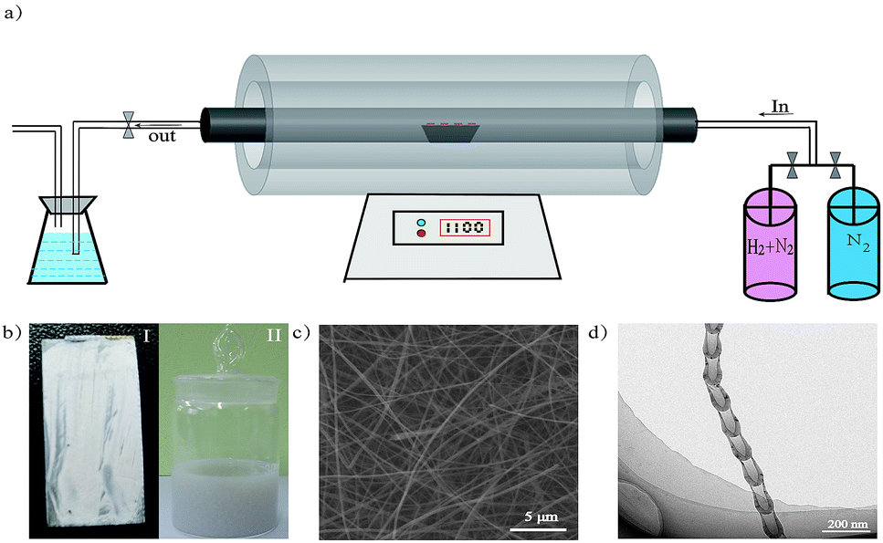 | ||
| Fig. 1 (a) Schematic diagram of the BNNT preparation system. (b) I shows a physical map of O-self-doped BNNTs on the substrate, II shows a high-purity O-self-doped BNNT suspension. (c) SEM image of the O-self-doped BNNTs (10 kV for SEM). (d) TEM images of the O-self-doped BNNTs (200 kV for TEM). | ||
A schematic diagram of the simplified preparation model in section view is shown in Fig. 2. The simplified growth mechanism of NTs involves five steps. The first step is to completely mix boron powders with the Fe2O3 nanoparticles. Next, the boron powders provide B raw materials for NTs and adsorb on the surface nano-Fe2O3 particles before annealing. The third step requires the following chemical reactions to occur on the surface of Fe2O3 nanoparticles during annealing:
 | (1) |
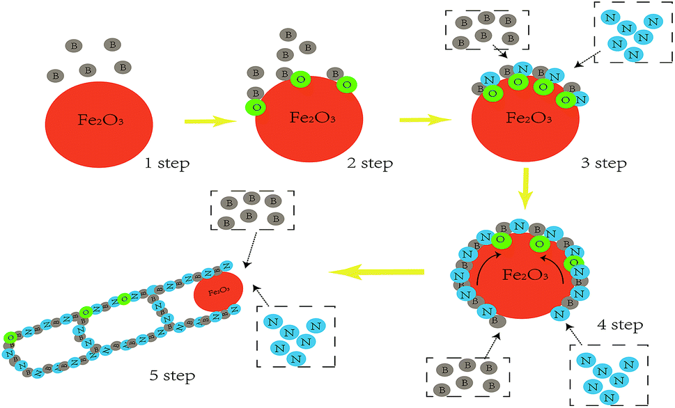 | ||
| Fig. 2 Schematic diagram of the growth mechanism of the NTs in a section view. | ||
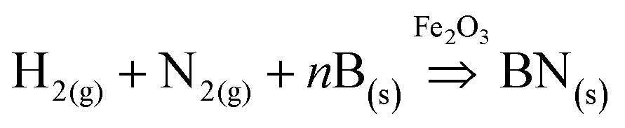
In these reactions, H2 is the activator, Fe2O3 is the catalyst, and BN localizes on the surface of the Fe2O3 nanoparticles. The next step is induced by the surface diffusion motion of BN on Fe2O3 nanoparticles to generate a full-closed BN shell layer on the surface.21 The final step uses capillarity effects to form the NTs at high temperature.22 During the growth process, we noted that the size of the catalyst nanoparticle and the annealing temperature substantially affected BNNT yield.23–25 In addition, during the fourth and fifth steps, some O elements were introduced into the BNNT crystal lattice, suggesting that the O element originates from Fe2O3 at the high temperature and randomly substitutes for B or N atoms during the annealing process in NTs.26 To analyze the role of O, X-ray photoelectron spectroscopy (XPS) was used to analyze the elements in the NTs, as shown in the Fig. 3a; the XPS results showed that O was present in the BNNTs. The XPS results were coincident. We fitted the B 1s peak with a scatter peak to determine the different bonds (the carbon peak at 284 eV comes from the environment, and rectification of the peak is required), which is shown in Fig. 3b. Moreover, the energy dispersive X-ray (EDX) results showed the doping atomic ratio of O in the O-self-doped NTs reached 7.34% (Fig. 3c) and the none-doped NTs reached 2.93% (Fig. 3d). Fig. 3c shows the EDX mapping analyse of single NT as a clear proofs to indicate the reality of oxygen doping. Combine with the results of the mapping analyse of none-doped BNNT, we suggest that the little O element was possible from the impurities of substrate. Based on the NIST X-ray Photoelectron Spectroscopy Database, the B–O and B–N–O bonds were included in the NTs, suggesting that O substitutes for B or N atoms randomly.27 Based on the results above, we confirm that the nano-Fe2O3 catalyzed annealing method efficiently synthesizes O-self-doped BNNTs with high purity.
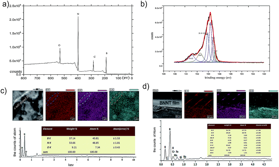 | ||
| Fig. 3 (a) The elementary composition of O-self-doped BNNTs film. (b) Survey images and a B 1s scan with the XPS-peak-differentiation-imitating analysis images of the O-self-doped BNNTs film. (c) EDX results and the elemental ratios of the O-self-doped BNNTs film, and the mapping analyse of the single NTs. (d) EDX results and element ratios of the pure BNNTs film and the mapping analyse of the film along the section orientation of substrate (NTs from the ball milling methods). | ||
To understand the improved conductivity of NTs after O doping, we first generated a physical model based on DFT to explain this effect.28 The (6, 0) and (8, 8) BNNT xyz coordinate files were built via the Virtual Nanolab as a precursor for simulation as shown in Fig. S1.†29 We used a generalized gradient approximation (GGA) Perde–Burke–Ernzerhof (PBE) model with an exchange-correlation energy and a SIESTA code based on the Linux system to obtain the band gap and DOS of the O-self-doped (6, 0 and 8, 8) BNNTs to compare with those of the non-doped BNNTs. We simulated substrates with O substituted for N (ON-doped) and B (OB-doped) as shown in Fig. S4.† After completing the calculations, the band gap of the doping lattice with oxygen decreased in the (8, 8) armchair and (6, 0) zigzag BNNTs as shown in Fig. S5.† A narrower band led to higher conductivity in the NT, which generated the observed increased current. All of the DOS and energy band structures from impurities were observed at the expected donor energy levels (refer to ESI† for details).
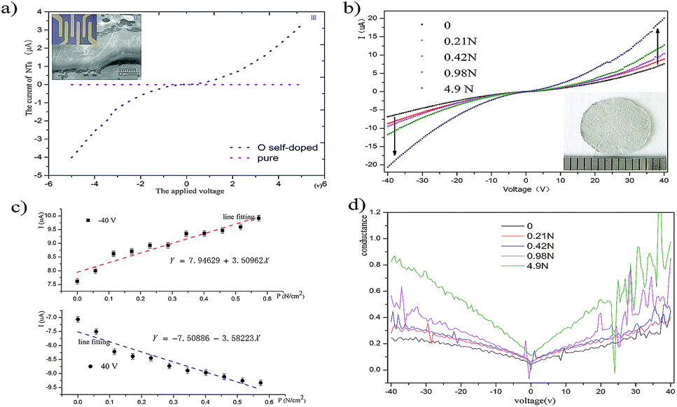
Next, we studied the electrical characteristics of O-self-doped BNNTs by high-precision equipment. We obtained a Ni/Au electrode with lift-off photolithography (Fig. 3-I) after the magnetron sputtering process in the prevacuum chamber (Fig. 3-II). As seen in Fig. 3a-III, the blue curve is the current of the O-self-doped NTs, which reached 4 μA at their highest and showed a test voltage range from −5 V to +5 V. Our results show that the electrical properties of the O-self-doped BNNTs improved substantially compared to the non-doped BNNTs (the red curves). Pure NTs were synthesized using our previous ball milling–annealing methods with a long milling time, as shown in Fig. 3d.20 To decrease the contact barrier, the testing electrode system required a crystallization process by annealing at 525 °C in air.30–32 Here, it seems that the Stark effect, the electron spin effect, or other quantum effects might account for the decreased barrier, but additional studies are required.33,34 According to the thermionic-field emission theory, the first order differential I–V curve is associated with NT resistance: R ≈ dV/dI.35 According to this first order differential equation, resistance has the value Rnon-doped ≈ 1.3 × 10⁹ Ω and RO-self-doped ≈ 0.85 × 10⁶ Ω. In general, conductance is the reciprocal of resistance, indicating that the electrical conductivity of O-doped BNNTs was much higher than that of non-doped BNNTs, and the results these tests are in agreement with the theory.
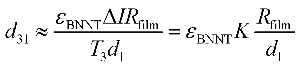
In view of the vast improvement in electrical properties, we characterized the piezoelectric properties of O-self-doped BNNT network film and calculated the piezoelectric voltage coefficient g31 based on piezoelectric constitutive equations (PCE) and apposite boundary conditions to explore potential in piezoelectric sensors.36,37 The thermal annealing condition was applied on the electrode to create the contact well, which is similar to a single NT. The network film was from the vacuum filtration of an ethanol suspension. Fig. 4b shows the I–V curves of NT network films under different pressures and that the current increases with increasing pressure. Obviously, the conductance of network film increases with pressure due to the piezoelectric effect, as shown in Fig. 4d. Fig. 4c shows the curves for film current I vs. stress S3 at 40 V and −40 V. The red line, K1, and the blue line, K2, in Fig. 4c are represented by the linear fitting slope at two different voltages; here, the slope K = ΔI/T (T for the stress) is relevant to the piezoelectric coefficient. The network film was sandwiched between the slide and the coverslip to maintain zero strain and electrically insulate the surroundings. Therefore, this experiment fitted to the third boundary condition of the piezoelectric equation.
 | ||
| Fig. 4 (a) I shows the electrode structure manufactured by the lift-off process, II shows the SEM image of the O-self-doped single NT contacting the electrode, and III shows the I–V curves of single O-self-doped (blue) and pure (purple) BNNTs in a voltage range of −5 to 5 V. (b) Piezoelectric properties of the BNNT network film under different forces and a physical map of the O-self-doped BNNT network film. (c) Images show the change in current with pressure at –40 V and 40 V, respectively. (d) The conductance vs. the voltage curves at the different pressures. | ||
The piezoelectric properties of the BNNTs come from their non-centrosymmetric hexagonal BN structure, and polarization resulting in piezoelectric properties can be strain controlled or stress controlled.38,39 It is known that the piezoelectric coefficient d31 is significantly correlated with piezoelectric effect performance. In addition, the piezoelectric coefficient indicates the polarization of a piezoelectric material upon application of a stress: d31 = D3/T1, in which D is the electric displacement, and T is the stress. For the linear electrical behavior of the material, D3 = εE3, in which ε is permittivity (free-body dielectric constant), and E is the electric field strength. Here, electric field E is related to resistivity and current density J, and current density J is related to current I. Therefore, the piezoelectric coefficient d31 was calculated using the follow equation:
 | (2) |
In which ΔI is the change of current, T3 is the load stress applied on the surface of the NTs film, and d1 is the electrode gap 1.5 mm. In addition, d31 = g31/εBNNT, with εBNNT approximately equal to 5.9 times vacuum permittivity. According to eqn (1) and the I–V curves of the film without stress, the resistance Rfilm ≈ 2.5 MΩ. Therefore, the piezoelectric coefficient d31 ≈ 31.186 pC N−1, and g31 ≈ −0.597 V m N−1. The values for the d31 coefficient are similar to other reports, and the g31 coefficient of the BNNT film is 2 times higher than the PVDF film (Max g31 = 0.28 V m N−1).40 Significantly, these sample methods might resolve the primary challenge in regard to measuring the piezoelectric constant.
Conclusions
In this article, high-quality O-doped BNNTs were fabricated using a nanocatalyst-assisted annealing method. This method makes the study of BN nano material fast. The O self-doped BNNT network films were prepared using a microporous filtration method, and the electrical properties of the O self-doped single BNNT and the network film were investigated using an I–V test and calculation. The conductivity of O-doped BNNTs was much higher than that of non-doped BNNTs, indicating that O markedly improves the electrical properties of BNNTs. We illustrated that the change in the energy band structure and DOS of O-self-doped BNNTs may cause increased electrical properties based on a first principle. The assessment of the BNNT film also clearly demonstrated its piezoelectric characteristics. This higher conductivity of piezoelectric O doped BN 1D nano material as a widely attraction material applied in the piezoelectric nano-devices, 1D electric nano-devices, and nano generator. Moreover, we calculated the piezoelectric constant d31 and g31 using a sample method. Herein, the g31 coefficient described the change in the electric field when stress was changed. The results show that BNNT network film had a higher piezoelectric voltage coefficient, indicating its high sensitivity to a supersonic wave compared to PVDF film. These results can guide the development of nano transducers, nano medicine and nano wearable devices.Conflicts of interest
There are no conflicts to declare.Acknowledgements
This work is financially supported by the Joint Space Science and Technology Fund (No. 6141B06260302), the National Natural Science Funds of China (Grant No. 61404036), and the State Key Laboratory of Urban Water Resource and Environment (Harbin Institute of Technology) (No. 2016TS 06).Notes and references
- D. Golberg, Y. Bando, K. Kurashima and T. Sato, Synthesis and Characterization of Ropes Made of BN Multiwalled Nanotubes, Scr. Mater., 2001, 44, 1561–1565 CrossRef.
- R. H. Baughman, C. Cui, A. A. Zakhidov, Z. Iqbal, J. N. Barisci, G. M. Spinks, G. G. Wallace, A. Mazzoldi, R. D. De and A. G. Rinzler, Carbon Nanotube Actuators, Science, 1999, 284, 1340 CrossRef PubMed.
- Y. Chen, J. Zou, S. J. Campbell and G. L. Caer, Boron Nitride Nanotubes: Pronounced Resistance to Oxidation, Appl. Phys. Lett., 2004, 84, 2430–2432 CrossRef.
- T. Terao, C. Zhi, Y. Bando, M. Mitome, C. Tang and D. Golberg, Alignment of Boron Nitride Nanotubes in Polymeric Composite Films for Thermal Conductivity Improvement, J. Phys. Chem. C, 2010, 114, 4340–4344 CrossRef.
- K. S. Kim, M. B. Jakubinek, Y. Martinez-Rubi, B. Ashrafi, J. Guan, K. O'Neill, M. Plunkett, A. Hrdina, S. Lin and S. Denommee, Polymer Nanocomposites from Free-Standing, Macroscopic Boron Nitride Nanotube Assemblies, RSC Adv., 2015, 5, 41186–41192 RSC.
- J. H. Kang, G. Sauti, C. Park, V. I. Yamakov, K. E. Wise, S. E. Lowther, C. C. Fay, S. A. Thiebeault and R. G. Bryant, Multifunctional Electroactive Nanocomposites Based on Piezoelectric Boron Nitride Nanotubes, ACS Nano, 2015, 9, 11942 CrossRef PubMed.
- K. Khoo, M. S. C. Mazzoni and S. G. Louie, Electronic Properties of Boron Nitride Nanotubes in the Presence of a Transverse Electric Field, in APS Meeting, 2003 Search PubMed.
- Y. Gu, X. Wang, W. Gu, Y. Wu, T. Li and T. Zhang, Flexible Electronic Eardrum, Nano Res., 2017, 10, 2683–2691 CrossRef.
- D. Golberg, Y. Bando, Y. Huang, T. Terao, M. Mitome, C. Tang and C. Zhi, Boron Nitride Nanotubes and Nanosheets, ACS Nano, 2010, 4, 2979–2993 CrossRef PubMed.
- Z. L. Wang, Novel Nanostructures of ZnO for Nanoscale Photonics, Optoelectronics, Piezoelectricity, and Sensing, Appl. Phys. A: Mater. Sci. Process., 2007, 88, 7–15 CrossRef.
- S. M. Nakhmanson, A. Calzolari, V. Meunier, J. Bernholc and M. B. Nardelli, Spontaneous Polarization and Piezoelectricity in Boron Nitride Nanotubes, Phys. Rev. B, 2003, 67, 102–105 CrossRef.
- Y. J. Chen, L. Fu, Y. Chen, J. Zou, J. Li and W. H. Duan, Tunable Electric Conductivities of Au-Doped Boron Nitride Nanotubes, Nano, 2008, 2, 367–372 CrossRef.
- K. L. Yao, Y. Min, S. C. Zhu, G. Y. Gao, Z. L. Liu and H. G. Cheng, First-Principles Study of Transport of V Doped Boron Nitride Nanotube, Phys. Lett. A, 2008, 372, 5609–5613 CrossRef.
- J. X. Zhao and B. Q. Dai, DFT Studies of Electro-Conductivity of Carbon-Doped Boron Nitride Nanotube, Mater. Chem. Phys., 2004, 88, 244–249 CrossRef.
- Q. Lu, Q. Zhao, T. Yang, C. Zhai, D. Wang and M. Zhang, Preparation of Boron Nitride Nanoparticles with Oxygen Doping and a Study of Their Room-Temperature Ferromagnetism, ACS Appl. Mater. Interfaces, 2018, 10, 12947–12953 CrossRef PubMed.
- J. Sahu, K. Panda, B. Gupta, N. Kumar, P. A. Manojkumar and M. Kamruddin, Enhanced Tribo-Chemical Properties of Oxygen Functionalized Mechanically Exfoliated Hexagonal Boron Nitride Nanolubricant Additives, Mater. Chem. Phys., 2018, 207, 412–422 CrossRef.
- M. Endo, H. Muramatsu, T. Hayashi, Y. A. Kim, M. Terrones and M. S. Dresselhaus, Nanotechnology: 'Buckypaper' from Coaxial Nanotubes, Nature, 2005, 433, 476 CrossRef PubMed.
- G. Gou, B. Pan and L. Shi, The Nature of Radiative Transitions in O-Doped Boron Nitride Nanotubes, J. Am. Chem. Soc., 2009, 131, 4839 CrossRef PubMed.
- J. F. S. Jr, P. J. Moses and S. Trolier-Mckinstry, The Wafer Flexure Technique for the Determination of the Transverse Piezoelectric Coefficient (d31) of PZT Thin Films, Sens. Actuators, A, 1998, 71, 133–138 CrossRef.
- L. Li, S. Fan, C. Zhuang, C. Ban and X. Liu, Customizable Local Superhydrophobic Micro Channels by BNNTs Growth, Microelectron. Eng., 2015, 141, 223–227 CrossRef.
- T. Hirano, T. Oku and K. Suganuma, Fabrication and Magnetic Properties of Boron Nitride Nanocapsules Encaging Iron Oxide Nanoparticles, Diamond Relat. Mater., 2000, 9, 476–479 CrossRef.
- L. T. Chadderton and Y. Chen, A Model for the Growth of Bamboo and Skeletal Nanotubes: Catalytic Capillarity, J. Cryst. Growth, 2002, 240, 164–169 CrossRef.
- R. Hoffmann, Solids and Surfaces, 1988 Search PubMed.
- K. Fujimura and A. Miyake, Effect of the Particle Size and Specific Surface Area of Ferric Oxide Catalyst on the Burning Rate of AP/HTPB Solid Propellant, Sci. Technol. Energ. Mater., 2010, 71, 65–69 Search PubMed.
- W. M. Shaheen, Effects of Thermal Treatment and Doping with Cobalt and Manganese Oxides on Surface and Catalytic Properties of Ferric Oxide, Mater. Chem. Phys., 2007, 101, 182–190 CrossRef.
- S. Abbas, A. Abbas, Y. Huang, J. Lin, Z. Liu, Y. Fang and C. Tang, Synthesis of Boron Nitride Nanotubes Using an Oxygen and Carbon Dual-Free Precursor, RSC Adv., 2018, 8, 3989–3995 RSC.
- US Department of Commerce, Nist X-Ray Photoelectron Spectroscopy Database 1, Version 2. NIST NSRDS Search PubMed.
- J. M. Soler, E. Artacho, J. D. Gale, A. Garcia, J. Junquera, P. Ordejon and D. Sanchez-Portal, The SIESTA Method for Ab Initio Order-N Materials Simulation, Physics, 2001, 14, 2745–2779 Search PubMed.
- E. Artacho, E. Anglada, O. Diéguez, J. D. Gale, A. García, J. Junquera, R. M. Martin, P. Ordejón, J. M. Pruneda and D. Sánchezportal, The SIESTA Method; Developments and Applicability, J. Phys.: Condens. Matter, 2008, 20, 064208 CrossRef PubMed.
- M. Radosavljevic, J. Appenzeller, V. Derycke, R. Martel, P. Avouris, A. Loiseau, J. L. Cochon and D. Pigache, Electrical Properties and Transport in Boron Nitride Nanotubes, Appl. Phys. Lett., 2003, 82, 4131–4133 CrossRef.
- K. B. Dhungana and R. Pati, Electrical Tuning of Spin Current in a Boron Nitride Nanotube Quantum Dot, Phys. Chem. Chem. Phys., 2014, 16, 7996 RSC.
- C. Kimura, T. Yamamoto and T. Sugino, Study on Electrical Characteristics of Metal/Boron Nitride/Metal and Boron Nitride/Silicon Structures, Diamond Relat. Mater., 2001, 10, 1404–1407 CrossRef.
- M. Ishigami, J. D. Sau, S. Aloni, M. L. Cohen and A. Zettl, Observation of the Giant Stark Effect in Boron-Nitride Nanotubes, Phys. Rev. Lett., 2005, 94, 056804 CrossRef PubMed.
- K. H. Khoo, M. S. C. Mazzoni and S. G. Louie, Tuning the Electronic Properties of Boron Nitride Nanotubes with Transverse Electric Fields: A Giant Dc Stark Effect, Phys. Rev. B, 2004, 69, 1324–1332 CrossRef.
- Z. Y. Zhang, C. H. Jin, X. L. Liang, Q. Chen and L. M. Peng, Current-Voltage Characteristics and Parameter Retrieval of Semiconducting Nanowires, Appl. Phys. Lett., 2006, 88, 073102 CrossRef.
- M. L. Thompson and H. A. Sosa, On the Material Properties and Constitutive Equations of Piezoelectric Poly Vinylidene Fluoride (PVDF), PhD thesis, Drexel University, 2002.
- Q. M. Wang and L. Eric Cross, Constitutive Equations of Symmetrical Triple Layer Piezoelectric Benders, IEEE Trans. Sonics Ultrason., 1999, 46, 1343–1351 Search PubMed.
- E. J. Mele and P. Král, Electric Polarization of Heteropolar Nanotubes as a Geometric Phase, Phys. Rev. Lett., 2002, 88, 056803 CrossRef PubMed.
- V. Yamakov, C. Park, H. K. Jin, K. E. Wise and C. Fay, Piezoelectric Molecular Dynamics Model for Boron Nitride Nanotubes, Comput. Mater. Sci., 2014, 95, 362–370 CrossRef.
- B. Gusarov, E. Gusarova, B. Viala, L. Gimeno and O. Cugat, PVDF Piezoelectric Voltage Coefficient In Situ measurements as a Function of Applied Stress, J. Appl. Polym. Sci., 2016, 133, 43248 CrossRef.
- J. P. Perdew, K. Burke and M. Ernzerhof, Errata: Generalized Gradient Approximation Made Simple, Phys. Rev. Lett., 1996, 77, 3865 CrossRef PubMed.
- M. Ernzerhof and G. E. Scuseria, Assessment of the Perdew–Burke–Ernzerhof Exchange-Correlation Functional, J. Chem. Phys., 1999, 110, 5029–5036 CrossRef.
Footnote |
| † Electronic supplementary information (ESI) available. See DOI: 10.1039/c8ra05698f |
| This journal is © The Royal Society of Chemistry 2018 |