
 Open Access Article
 This Open Access Article is licensed under a Creative Commons Attribution-Non Commercial 3.0 Unported Licence
Ultrasensitive detection of low-ppm H2S gases based on palladium-doped porous silicon sensors†
Nu Si A. Eom‡
ab,
Hong-Baek Cho‡b,
Hyo-Ryoung Limb,
Tea-Yeon Hwangb,
Yoseb Songb and
Yong-Ho Choa *b
*b
aElectrochemistry Department, Korea Institute of Materials Science, Changwon, 51508, Republic of Korea
bDepartment of Fusion Chemical Engineering, Hanyang University, Ansan, 15588, Republic of Korea. E-mail: choa15@hanyang.ac.kr; Fax: + 82 31 418 6490; Tel: +82 11 9629 7446
First published on 24th August 2018
Abstract
In this study, the sensing properties of palladium-doped porous silicon (Pd/p-Si) substrates for low-ppm level detection of toxic H2S gas are investigated. A Si substrate with dead-end pores ranging from nano- to macroscale was generated by a combined process of metal-assisted chemical etching (MacE) and electrochemical etching with tuned reaction time, in which nano-Pd catalysts were decorated by E-beam sputtering deposition. The sensing properties of the Pd/p-Si were enhanced as the thickness of the substrate layer increased; along with the resulting variation in surface area, this resulted in superior H2S sensing performances in the low-ppm range (less than 3 ppm), with a detection limit of 300 ppb (sensitivity 30%) at room temperature. Furthermore, the sensor displayed excellent selectivity toward the hazardous H2S molecules in comparison with various other reducing gases, including NO2, CO2, NH3, and H2, showing its potential for application in workplaces or environments affected by other toxic gases. The enhancement in sensing performance was possibly due to the increased dispersion and surface area of Pd nano-catalysts, which led to an increase in chemisorption sites of adsorbate molecules.
Introduction
In the past few decades, due to rapid industrialization and urbanization, the development of gas sensors has attracted continuous attention in areas such as environmental monitoring, agriculture, disease diagnosis, household security, and vehicles.1–3 The detection of gases such as H2S, SO2, and NH3, which can be harmful to human health, is necessary in many fields, especially environmental monitoring and process control, due to their toxicity and associated risk to the ecosystem.4,5 In addition to the various toxic and/or combustible gaseous and liquid products generated at chemical and materials processing plants, ensuring security at airports and other public sites is a clear motivation for tracking and controlling such emissions of chemical analytes.6 Therefore, there is high demand for high-performance sensors for monitoring harmful gas. A promising basis for high-performance sensing devices is nanomaterials and nanostructures7 because the key factors in improving gas sensing performance are improving the interaction between the gas molecules and the sensing surface and decreasing the operating temperature.8 Nanostructured materials exhibit excellent sensing properties because they improve the adsorbate molecule-to-sensing surface interaction through their high surface area-to-volume ratio.9–11Among the various possible nanomaterials, porous silicon (p-Si) is an interesting base material for developing a gas sensor due to its unique combination of crystalline structure; high specific surface area of up to 200–800 m2 g−1, which enables the enhancement of adsorbate effects; and high surface chemical activity.12,13 Because of these features, p-Si has been used as a template for the detection of many gases, such as NO2, NH3, H2S, SO2, CO, and more.14,15 Compared to other semiconductor gas sensors, p-Si chemical sensors can be operated at relatively low temperatures, even room temperature,16 due to their high specific surface area and high surface chemical activity.17 The sensing principles of p-Si gas sensors are generally associated with changes in the carrier concentration18,19 in the porous layer or changes in the dielectric constant20,21 between the p-Si surfaces and the detecting gas due to intrinsic adsorption properties and the concentration of the gas.
The properties of p-Si gas sensors are strongly dependent on their surface morphology. It is essential to synthesize the p-Si sensor by controlling the structural morphology, creating porosity in porous layers of controlled thickness in order to improve the efficiency and sensing properties of the device. These sensors have been used for detecting low concentrations of ecologically harmful gases. Hydrogen sulfide, H2S, is one example of such a gas, of which concentrations between 15 and 100 ppm are considered to cause severe damage to human health in the form of digestive upset, loss of appetite, olfactory paralysis, and eye and/or lung irritation.22 This necessitates the monitoring and detection of H2S and the control of its leakage in many technological processes;23 therefore, the development of stable and reliable H2S gas sensor systems with high sensitivity and selectivity is crucial.
To enhance the selectivity of Si-based gas sensors, various additives such as graphene,24 Pd,25 CuO,26 and WO3 (ref. 27) have been incorporated into p-Si. Pd particles are mainly used as H2 sensing materials and form PdHx upon exposure to H2 gas molecules through dissociative adsorption, resulting in changes in the resistance of the substrate.28 It is extensively used as a catalyst metal for the enhancement of H2S gas adsorption over a wide range of temperatures and enables detection even at room temperature.29,30 Hydrogen sulfide gas also shows dissociative adsorption at the surface of the catalytic Pd clusters, then diffuses before interacting with other reacting adsorbate oxygen species in atmospheric conditions.31,32 Recently, the interaction mechanisms of H2S molecules with other types of metal surfaces have been studied.33 However, there has been little significant research on H2S gas sensors using Pd/p-Si at room temperature.
In this study, we investigated a Pd/p-Si substrate-based gas sensor for low-ppm H2S gas detection at room temperature. The Pd/p-Si gas sensor was synthesized on silicon wafer substrates by an electrochemical etching process to control porosity as a function of etching time. The deposition of nanoscale palladium particles was carried out by E-beam evaporation to produce a homogeneous distribution of active sites. The sensing properties for H2S gas molecules were analyzed in combination with the interaction between the p-layers of silicon and the Pd particles. The synthesized gas sensor had 30% sensitivity under exposure to 300 ppb of H2S at room temperature and displayed remarkable selectivity for H2S detection in comparison with other gases.
Experimental
The high porosity silicon substrate was fabricated on a p-type monocrystalline silicon wafer with a thickness of 300 μm, orientation of 〈100〉, and resistance of 1–10 Ω by combining the processes of metal-assisted chemical etching (MacE) and electrochemical etching. To remove organic contamination and the oxide layer on the Si surface, the Si substrates were dipped in 6![[thin space (1/6-em)]](https://www.rsc.org/images/entities/char_2009.gif) :3:1 volume ratio of H2SO4:H2O2:H2O for 10 min at 80 °C, followed by 10 wt% HF for 10 min. The samples were washed with deionized water and dried under an ambient nitrogen gas flow. The deposition of Pt catalyst on the prepared silicon was carried out by sputtering deposition of a Pt (purity: 99.99%) target using sputtering equipment (Quorum Technologies, Q150T, ES). The regions of deposited Pt metal particles on the Si substrate had nanoscale dimensions ranging from 30–60 nm after deposition and heat treatment at 650 °C (see Fig. S1 in ESI†), and the Pt particles had an effect on the p-layer morphology of the silicon wafer surface during the combined MacE and electrochemical etching technique.34,35 After cooling to room temperature, the Pt-doped silicon wafer was attached to aluminum foil for electrochemical etching, in which the anodic bath was composed of a mixture of 30 wt% H2O2 and 10 wt% HF, and the Si (metal plate) and Pt were connected to a computer-controlled DC power supply (E3647A, Agilent) as working electrode and counter electrode, respectively. A current density of 1 mA cm−2 was applied, and the time for porosity generation was varied from 10 to 120 minutes during the electrochemical etching in the HF–H2O2 solution. The resulting porous silicon substrate was then dipped in 10 wt% HF for 10 seconds in order to remove the oxide layer that formed on the silicon surface during the anodizing process, and the samples were rinsed thoroughly in DI water and dried at room temperature. To form a Pd layer with thickness of approximately 3 nm on the prepared p-Si surface, sputtering deposition of a Pd (purity: 99.99%) target was carried out using E-beam evaporation (UEE, ULTECH, Korea). A gold layer of 200 nm thickness was deposited on the top of each p-Si surface as a sensor electrode to create an ohmic electrical contact, which was confirmed by the current–voltage (IV) curve (NI PXle-1073, National Instruments Corporation, USA). The morphology of the Pd-doped p-Si sample was analyzed by scanning electric microscopy (SEM, MIRA3, TESCAN Ltd., USA). The phase analysis of Pd on the silicon substrate was carried out using SEM-EDX (MIRA3, TESCAN Ltd., USA) and X-ray fluorescence (XRF, Rigaku Co. Ltd, Tokyo, Japan). The metal dispersion and metal surface area of the deposited Pd catalyst on porous silicon wafer substrate were confirmed by a H2 chemisorption method (ASAP 2020, Micromeritics Inc., USA). The electrical and gas sensing properties of the sensor system were measured and recorded online, and the periodic changes in electrical response between dry air and the detecting gases (H2S, NO2, NH3, CO2, and H2) were compared at room temperature. The pore diameter distribution of the p-Si substrate was obtained by measurements of 50 pore sizes from each SEM image using image analysis software (ImageJ). The resistance of the sensor was measured by a NI PXle-1073 (National Instruments Corporation, USA).
:3:1 volume ratio of H2SO4:H2O2:H2O for 10 min at 80 °C, followed by 10 wt% HF for 10 min. The samples were washed with deionized water and dried under an ambient nitrogen gas flow. The deposition of Pt catalyst on the prepared silicon was carried out by sputtering deposition of a Pt (purity: 99.99%) target using sputtering equipment (Quorum Technologies, Q150T, ES). The regions of deposited Pt metal particles on the Si substrate had nanoscale dimensions ranging from 30–60 nm after deposition and heat treatment at 650 °C (see Fig. S1 in ESI†), and the Pt particles had an effect on the p-layer morphology of the silicon wafer surface during the combined MacE and electrochemical etching technique.34,35 After cooling to room temperature, the Pt-doped silicon wafer was attached to aluminum foil for electrochemical etching, in which the anodic bath was composed of a mixture of 30 wt% H2O2 and 10 wt% HF, and the Si (metal plate) and Pt were connected to a computer-controlled DC power supply (E3647A, Agilent) as working electrode and counter electrode, respectively. A current density of 1 mA cm−2 was applied, and the time for porosity generation was varied from 10 to 120 minutes during the electrochemical etching in the HF–H2O2 solution. The resulting porous silicon substrate was then dipped in 10 wt% HF for 10 seconds in order to remove the oxide layer that formed on the silicon surface during the anodizing process, and the samples were rinsed thoroughly in DI water and dried at room temperature. To form a Pd layer with thickness of approximately 3 nm on the prepared p-Si surface, sputtering deposition of a Pd (purity: 99.99%) target was carried out using E-beam evaporation (UEE, ULTECH, Korea). A gold layer of 200 nm thickness was deposited on the top of each p-Si surface as a sensor electrode to create an ohmic electrical contact, which was confirmed by the current–voltage (IV) curve (NI PXle-1073, National Instruments Corporation, USA). The morphology of the Pd-doped p-Si sample was analyzed by scanning electric microscopy (SEM, MIRA3, TESCAN Ltd., USA). The phase analysis of Pd on the silicon substrate was carried out using SEM-EDX (MIRA3, TESCAN Ltd., USA) and X-ray fluorescence (XRF, Rigaku Co. Ltd, Tokyo, Japan). The metal dispersion and metal surface area of the deposited Pd catalyst on porous silicon wafer substrate were confirmed by a H2 chemisorption method (ASAP 2020, Micromeritics Inc., USA). The electrical and gas sensing properties of the sensor system were measured and recorded online, and the periodic changes in electrical response between dry air and the detecting gases (H2S, NO2, NH3, CO2, and H2) were compared at room temperature. The pore diameter distribution of the p-Si substrate was obtained by measurements of 50 pore sizes from each SEM image using image analysis software (ImageJ). The resistance of the sensor was measured by a NI PXle-1073 (National Instruments Corporation, USA).
Results and discussion
Fig. 1 shows the surface and cross-sectional morphologies of p-Si wafers for etching times of 10, 30, 60, and 120 min in the electrochemical process. The thickness and diameter of the synthesized p-layers gradually increased with etching time and were generated uniformly across the entire substrate surface. With an etching time of 10 min, a porous layer of dead-end porosity with a thickness of 15 μm was created. The thickness increased to 40 μm, 90 μm, and 140 μm as the etching time was extended to 30 min, 60 min, and 120 min, respectively. The cross-sectional images show that the porous layers were firmly attached to the substrate with vertically upright assembly. The insets of Fig. 1(a)–(d) show that the average pore diameter increased with the increase in etching time; the mean pore diameter after 10 min of etching was 1.5 μm, which proportionally increased to 2.3, 4.5, and 5.6 μm as the etching time increased from 10 to 120 min. The magnified view of the inside wall of the internal pores show narrower nanoscale gaps on the surface, indicating the microporosity of the p-Si substrate (Fig. S2†).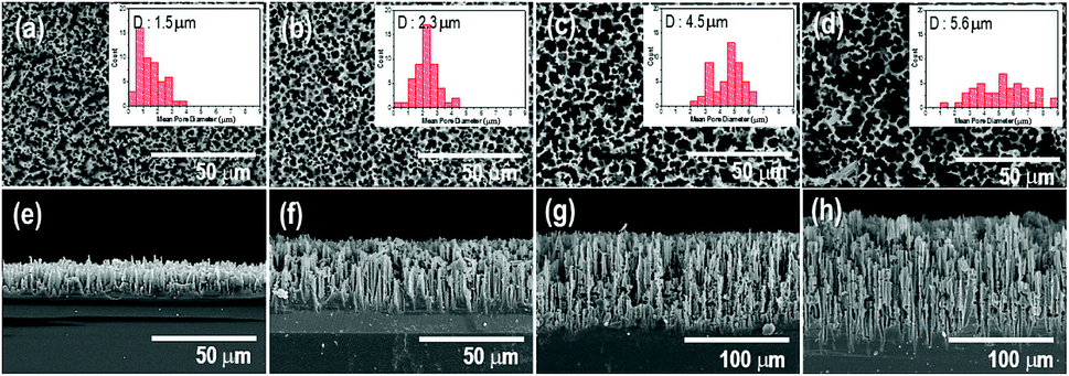 | ||
| Fig. 1 Surface and cross-sectional SEM images of the Pd-doped porous layer of Si wafer substrates with varying thickness; (a) and (e) 15 μm, (b) and (f) 40 μm, (c) and (g) 90 μm, and (d) and (h) 140 μm. | ||
Fig. 2 compares the sensitivity of the sensing properties of the fabricated Pd deposited sensor system as a function of etching time under a 10 ppm dose of H2S gas. With increasing porous layer thickness and pore diameter, the sensing properties increased to an etching time of 60 min and then decreased with longer etching times upon exposure to H2S gas. The enhancement in these sensing properties was related to the increased surface area of the p-Si template and the extended domains allowing palladium nanoparticle deposition through the increase in interaction sites with H2S gas molecules. The increase in resistance due to the adsorption of hydrogen sulfur gas was not observed when a non-Pd-doped p-Si substrate was used (see also Fig. S2 in ESI†). In contrast, the palladium-doped porous silicon with p-Si layer thicknesses of 15 μm, 40 μm, and 90 μm (in Fig. 2(a)–(c)) showed an increase in resistance under 10 ppm of H2S gas injection. Although the p-Si substrate with a porous layer thickness of 140 μm had H2S sensing performance of around 0.7 × 10³ Ω, it was similar to the gas response (Rg/Ra) of p-Si with a 15 μm-thick porous layer, as shown in Fig. S4.† It is surmised that the collapsed porosity due to excessive etching and the inevitable decrease in deposition sites for Pd metal during Pd deposition directly influenced the poor sensing properties of H2S gas molecules on the p-Si layer. Eqn (1) describes the surface reaction that occurs when H2S gas approaches the silicon surface, a surface oxidation reaction with adsorbed oxygen species (O2−, O−, O2−):36
| 2H2S(g) + 3O2(ad)α− ↔ 2H2O(g) + 2SO2(g) + 3αe− (α = 1, 2) | (1) |
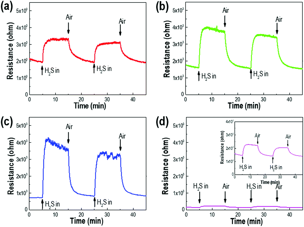 | ||
| Fig. 2 The resistance changes of Pd/p-Si sensors as a function of etching time; (a) 10 min, (b) 30 min, (c) 60 min, and (d) 120 min, under exposure to 10 ppm H2S. | ||
In this reaction, the electrons formed by the chemisorption of detecting gas molecules and the holes from the p-type Si substrate generate an electron–hole pair, resulting in reduced conductance (or enhanced resistance). The hole density of p-type silicon is controlled by the surface reaction of H2S with chemisorbed oxygen species on the sensing material's surface.
Fig. 3(a) and (b) show TEM-EDX spectra and mappings of the 3 nm Pd-doped porous layer of 15 μm thickness on the Si substrate. The TEM-EDX spectra confirm the presence of Pd on the porous layered Si, with a concentration of approximately 1 at%. It was also confirmed that over 4.5 at% of Pt particles remained on the Si porous layer after the anodization process during electrochemical etching. This did not impact the sensing properties, as shown by the lack of resistance variation in Fig. S3 in ESI.† As an identical amount of Pd was deposited on the porous silicon substrate, a disparity in sensing properties of the porous silicon substrate was expected due to the dispersion and surface area of the deposited Pd being influenced by the structural morphology of the porous layer, as shown in Fig. 3(c) (see also the ESI† for information on the Pd content calculation). The relative dispersion of Pd particles on the surface of the porous Si layer increased for a porous layer thickness of 90 μm relative to that of the sample with thickness of 15 μm by an amount proportional to the increase in metal surface area. This confirms that the increase in porosity and layer thickness of Si substrate attributed to the substantial increase in dispersion and surface area of the doped palladium, leading to enhanced sensing performance.
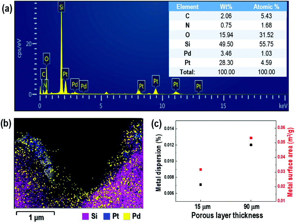 | ||
| Fig. 3 (a) EDX-TEM and (b) TEM analysis of a 3 nm Pd-doped 15 μm-thick porous layer on silicon substrate, and (c) 3 nm Pd dispersion on 300 μm Si wafers with porous layer thickness of 15 μm and 90 μm. | ||
The IV behavior of the samples can be explained using the energy band diagram shown in Fig. 4. Both the synthesized pure p-Si and the P/p-Si showed the formation of an ohmic contact between the substrate and the Au electrodes (Fig. 4(a)). The ohmic contact between Pd and p-Si is explained by the formation of a hetero-junction, as determined by the energy band diagram shown in Fig. 4(b). This ohmic response was expected because the work function of palladium (φPd) is 5.12 eV, which is higher than that of p-Si (∼4.97 eV), and the electron affinity (χSi) and bandgap of Si are 4.05 and 1.12 eV, respectively.37 Therefore, the Ef − Ev is estimated to be ∼0.2 eV based on a resistivity of 1–10 Ω cm for p-type Si.24 This ohmic behavior is very important to the gas sensing properties because the sensitivity of the gas sensor, the ratio of the electrical resistance under H2S gas to that under dry air, can be maximized38,39 depending on the contact resistance. After a contact barrier is formed due to the work function disparity between Pd particles and the p-Si interface, partial carriers in the p-Si move toward the Pd side, leading to the formation of a hole accumulation layer.
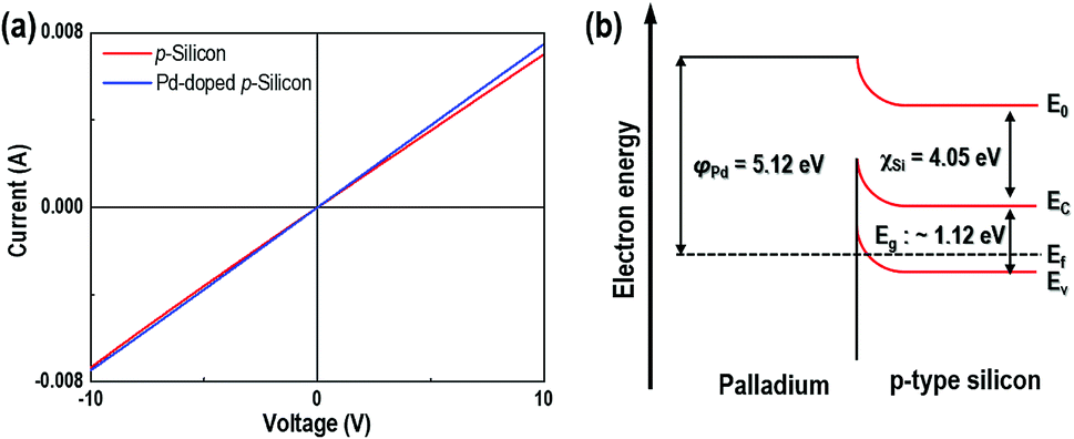 | ||
| Fig. 4 (a) IV curve and (b) band diagram between palladium and p-type silicon in a Pd/p-Si wafer. | ||
The variation in resistance change under exposure to H2S gas was measured to demonstrate the potential utility of the gas-sensing properties of the Pd/p-Si (see Fig. 5). The sensor system with a 90 μm-thick porous layer was chosen to evaluate the sensing properties before and after introducing the detecting gas at atmospheric temperature. The resistance of the materials increased upon exposure to H2S, indicating that the decorated p-Si substrate was a p-type semiconducting oxide. The response time is defined as the time to achieve 90% of the stable output of the sensor after the detected gas enters, while the recovery time is defined as the time to fall to 10% of its maximum output after the detected gas exits.40 A response time of 65 s was measured during exposure to 10 ppm H2S gas; when the gas was removed, the resistance of the sensor decreased with a recovery time of 165 s. A comparison between the sensing performance of this sensor system and literature reports is summarized in Table S1.† It is inferred that the increase in surface area and Pd adsorption sites motivated the fast response and recovery of the interaction with H2S gas.
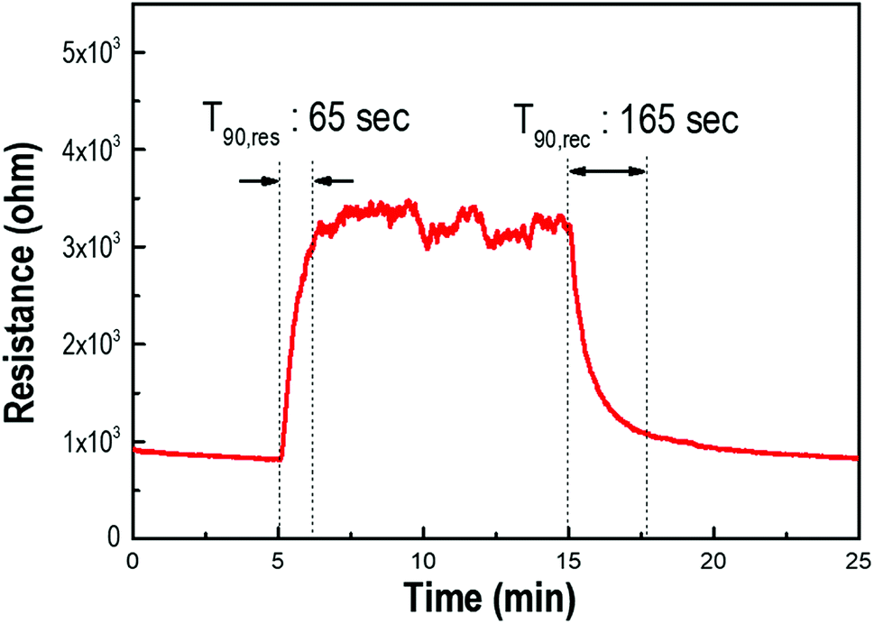 | ||
| Fig. 5 The response and recovery behavior of the Pd-doped porous Si layer of 90 μm thickness under exposure to 10 ppm of H2S gas at room temperature. | ||
The typical response–recovery curves of the samples were further investigated by sequentially exposing the sensor to different concentrations of H2S between 0.3 ppm to 3 ppm at room temperature, as shown in Fig. 6. Sensitivity was defined as ΔR/Ra = (Rg − Ra)/Ra × 100, where Ra and Rg represent the resistance of the sensor exposed to air and H2S gas, respectively. Fig. 6 shows the variation in sensitivity, which proportionally increased to 30, 50, 70, 110, 150, 330, and 500 for introduced gas concentrations of 0.3, 0.5, 0.7, 1, 1.5, 2, and 3 ppm, respectively. The response and recovery characteristics were almost reproducible. The sensor system had relatively fast response and recovery time, indicating the rapid changes in resistance upon exposure to H2S gas and air. It is obvious that the palladium-doped sensor was able to detect a wide range of H2S concentrations with a detection limit at the ppb level; the response toward 300 ppb (0.3 ppm) H2S was still as high as 30% sensitivity, indicating that the sensor can detect H2S gas down to the ppb level. Furthermore, the sensor sensitivity could completely recover to its initial value rapidly, suggesting that the sensor could monitor H2S gas at a sub-ppm level at room temperature.
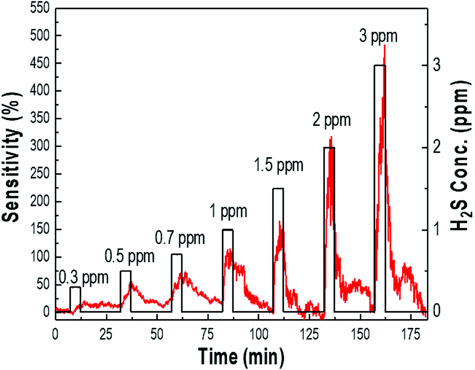 | ||
| Fig. 6 The sensing response curves of the Pd/p-Si with 90 μm thickness for different concentrations of H2S at room temperature. | ||
Gas selectivity is one of the crucial properties in determining whether a sensor can respond selectively to a group of analytes or even specifically to a single analyte.41 To examine the H2S gas selectivity of the decorated p-Si gas sensor, the sensing response to other gases, including CO2, NH3, NO2, and H2, was examined and compared with the response to H2S. Fig. 7 shows the sensor response to H2S gas and other gases measured at room temperature. Here, the sensor response was calculated by S = ΔR/Rg × 100 for reductive gases such as NH3 or H2 and as S = ΔR/Ra × 100 for oxidizing gases such as NO2 or CO2 because the conductance of the p-Si switched depending on whether the target gases adsorbed on the surface as oxidizing or reducing agents. Fig. S5† exhibits the sensitivity of the Pd/p-Si gas sensor to CO2, NH3, NO2, and H2, as well as the gas concentration at room temperature. As shown in Fig. 7, the Pd/p-Si sensor showed the highest response of 90% for H2S gas at the lowest concentration of 3 ppm, while the responses to 10000 ppm CO2, 333 ppm NH3, 20 ppm NO2, and 1000 ppm H2 were 5%, 10%, 50%, and 30%, respectively. The metal doped porous silicon sensors have been generally used for detection of H2 gas molecules as summarized in Table S2† because of the selectivity of porous silicon substrate toward H2 gas molecules at room temperature. However, we could accomplish a novel demonstration of excellent sensing selectivity toward H2S (response of 90% to 3 ppm H2S gas corresponding to 5% to 1000 ppm H2 gas) by sophisticated control of Pd deposition on the surface of highly porous silicon. It can be concluded that the Pd/p-Si gas sensor has excellent sensing selectivity to H2S compared to other reducing gases, demonstrating its potential for detecting H2S gas in complex environments and even enabling it to monitor extremely dilute leakage of the gas.
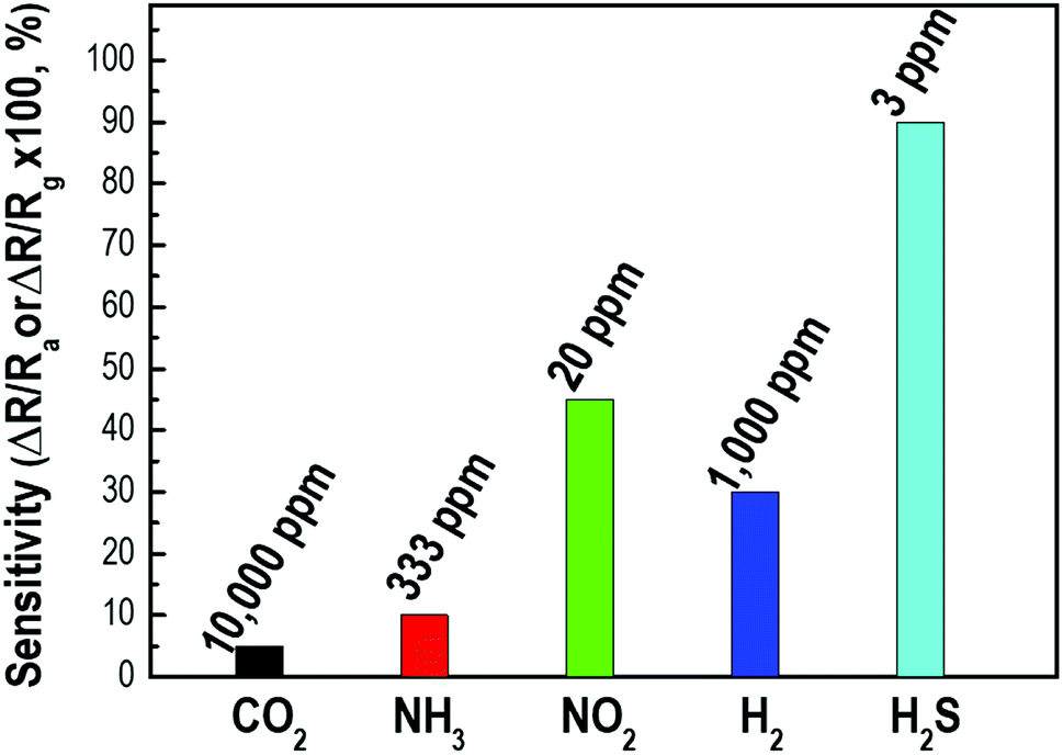 | ||
| Fig. 7 The selectivity of a Pd-doped p-Si gas sensor of 90 μm thickness for various detecting gases at room temperature. | ||
The Pd/p-Si has excellent sensing properties due to the high specific surface area of the chemical activity on the p-Si surface, which was verified by H2S chemisorption (Fig. 5). Fig. 8 shows a schematic illustration of the gas sensing mechanism of Pd/p-Si in H2S gas and in air. As previously mentioned in Fig. 4(b), some electrons in p-Si move to the higher work function of Pd due to the formation of an ohmic junction between Pd and p-Si, which results in the formation of a hole accumulation layer near the Pd/p-Si interface. When the Pd/p-Si sensor is exposed to H2S gas (a reducing gas), the gas molecules adsorb on the active sites of the Pd nanoparticles, preferentially taking an electron in the process. The catalytic palladium metals dispersed on the p-Si enhance the dissociative adsorption of H2S molecules through the spill-over effect, leading to an increase in the rate of dissociation and resulting in chemisorption between the detecting gas and the sensor materials,42 in which the H2S molecules dissociate into hydrogen and sulfur atoms on the Pd particles and then diffuse to the substrate.31,32 The resulting hydrogen atoms partly penetrate the Pd metal film to the Pd/p-Si interface,30 and the accumulated holes near the Pd/p-Si interface and the absorbed gas molecules are transferred. Consequently, the adsorption of H2S on the surface of the Pd/p-Si results in an increase in resistivity.
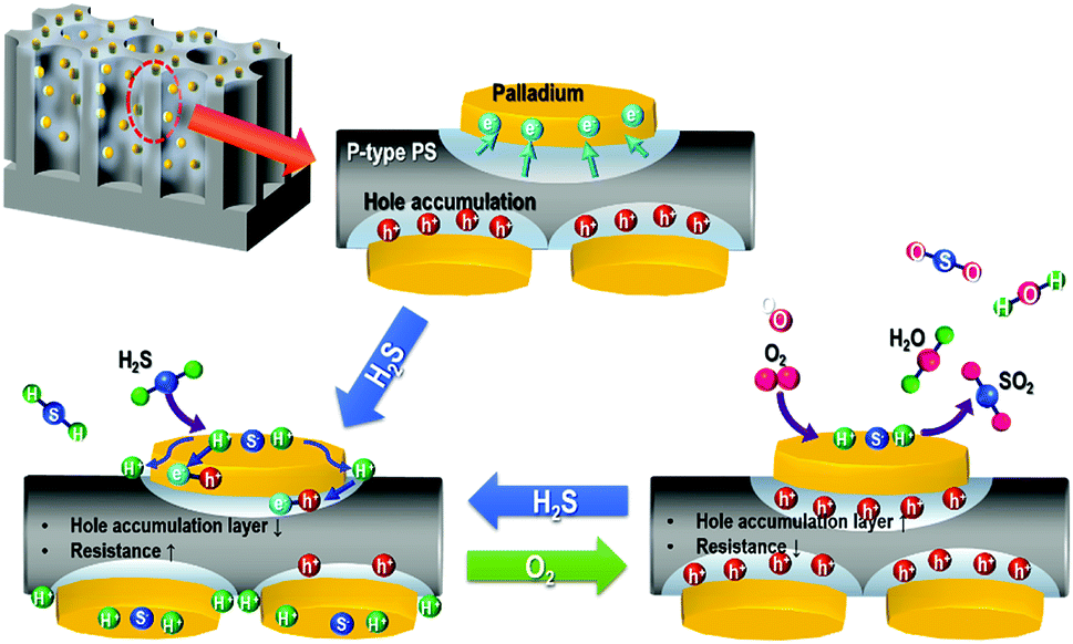 | ||
| Fig. 8 Schematic of the H2S gas sensing performance of Pd/p-Si sensors through surface oxidation in air at room temperature. | ||
In contrast, when the Pd/p-Si is exposed to air, the electrons in the Pd and p-Si are trapped by oxygen molecules, which can form ionized oxygen species through oxygen redox reactions and undergo a surface reaction with chemisorbed hydrogen and sulfur atoms on the surface of the Pd and the p-Si substrate adjacent to the edges of the Pd metal, leading to hole transfer into the valence band of the Si. The holes accumulated in the Pd/p-Si then enhance the conductance. The unique surface morphology, which ranged from nano- to macroporosity, enabled the metal-doped porous silicon to possess an increased surface area throughout the entire p-Si surface, providing the synergic effect necessary to obtain excellent sensing properties in the sensor system.
Conclusions
A noticeable enhancement in both H2S gas sensitivity and selectivity was demonstrated by Pd-decorated Si substrates with nano- to macroporosity and high surface area. The porosity of the p-Si could be tuned using an electrochemical etching process, which enabled control of the thickness of the porous silicon layers from 15 μm to 140 μm by varying the etching time. The sensing properties of the synthesized Pd/p-Si substrate were noticeably improved with an increase in the porous layer thickness, with maximum sensitivity at a thickness of 90 μm, due to an increase in Pd dispersion that enhanced the surface oxidation of the adsorbate molecules. The Pd/p-Si sensors exhibited high sensitivity at low H2S concentrations less than 3 ppm, with a detection limit of 300 ppb (sensitivity of 30%) at room temperature. Furthermore, the Pd/p-Si gas sensor had excellent sensing selectivity toward H2S compared to other reducing gases (NO2, NH3, CO2, and H2), demonstrating its potential for application in complex environments and even its ability to monitor extremely dilute leakage of the gas.Conflicts of interest
There are no conflicts to declare.Acknowledgements
This research was supported by Nano Material Technology Development Program (No. 2016M3A7B4900044) and the Basic Science Research Program (No. 2015R1A5A1037548) funded by the National Research Foundation of Korea (NRF) and the Ministry of Science, ICT & Future Planning, Republic of Korea.References
- S. G. Chatterjee, S. Chatterjee, A. K. Ray and A. K. Chakraborty, Graphene–metal oxide nanohybrids for toxic gas sensor: a review, Sens. Actuators, B, 2015, 221, 1170–1181 CrossRef.
- P. Rai, S. Raj, K.-J. Ko, K.-K. Park and Y.-T. Yu, Synthesis of flower-like ZnO microstructures for gas sensor applications, Sens. Actuators, B, 2013, 178, 107–112 CrossRef.
- T. Wagner, S. Haffer, C. Weinberger, D. Klaus and M. Tiemann, Mesoporous materials as gas sensors, Chem. Soc. Rev., 2013, 42, 4036–4053 RSC.
- Z. Hosseini, A. Mortezaali and S. Fardindoost, Sensitive and selective room temperature H2S gas sensor based on Au sensitized vertical ZnO nanorods with flower-like structures, J. Alloys Compd., 2015, 628, 222–229 CrossRef.
- S. A. Hooker, Nanotechnology advantages applied to gas sensor development, in The nanoparticles 2002 conference proceedings, 2002, pp. 1–7 Search PubMed.
- I.-D. Kim, A. Rothschild and H. L. Tuller, Advances and new directions in gas-sensing devices, Acta Mater., 2013, 61, 974–1000 CrossRef.
- G. Di Francia, B. Alfano and V. La Ferrara, Conductometric gas nanosensors, J. Sens., 2009, 18 Search PubMed.
- Y. Wang, B. Liu, S. Xiao, H. Li, L. Wang, D. Cai, D. Wang, Y. Liu, Q. Li and T. Wang, High performance and negative temperature coefficient of low temperature hydrogen gas sensors using palladium decorated tungsten oxide, J. Mater. Chem. A, 2015, 3, 1317–1324 RSC.
- N. S. Ramgir, Y. Yang and M. Zacharias, Nanowire Based Sensors, Small, 2010, 6, 1705–1722 CrossRef PubMed.
- Y. Wang, J. Liu, X. Cui, Y. Gao, J. Ma, W. Sun, P. Sum, F. Liu, X. Liang, T. Zhang and G. Lu, NH3 gas sensing performance enhanced by Pt-loaded on mesoporous WO3, Sens. Actuators, B, 2017, 238, 473–481 CrossRef.
- T. Yang, Q. YANG, Y. Xiao, P. Sun, Z. Wang, Y. Gao, J. Ma, Y. Sun and G. Lu, pulse-driven sensor based on ordered mesoporous Ag2O/SnO2 with improved H2S-sensing performance, Sens. Actuators, B, 2016, 228, 529–538 CrossRef.
- S. E. Lewis, J. R. DeBoer, J. L. Gole and P. J. Hesketh, Sensitive, selective, and analytical improvements to a porous silicon gas sensor, Sens. Actuators, B, 2005, 110, 54–65 CrossRef.
- G. Korotcenkov, Handbook of gas sensor materials, Springer, Heidelberg 2013 Search PubMed.
- L. T. Canham, Properties of porous silicon, INSPEC, London, UK, 1997 Search PubMed.
- C. Baratto, E. Comini, G. Faglia, G. Sberveglieri, G. Di Francia, F. De Filippo, V. La Ferrara, L. Quercia and L. Lancellotti, Gas detection with a porous silicon based sensor, Sens. Actuators, B, 2000, 65, 257–259 CrossRef.
- V. Solntsev, V. Litovchenko, T. Gorbanyuk and A. Evtukh, Influence of H2S and H2 adsorption on characteristics of MIS structures with Si porous layers, Semicond. Phys., Quantum Electron. Optoelectron., 2008, 11, 381–384 Search PubMed.
- S. Ozdemir and J. L. Gole, The potential of porous silicon gas sensors, Curr. Opin. Solid State Mater. Sci., 2007, 11, 92–100 CrossRef.
- K. Watanabe, T. Okada, I. Choe and Y. Sato, Organic vapor sensitivity in a porous silicon device, Sens. Actuators, B, 1996, 33, 194–197 CrossRef.
- S.-J. Kim, S.-H. Lee and C.-J. Lee, Organic vapour sensing by current response of porous silicon layer, J. Phys. D: Appl. Phys., 2001, 34, 3505–3509 CrossRef.
- R. C. Erson, R. S. Muller and C. W. Tobias, Investigations of porous silicon for vapor sensing, Sens. Actuators, A, 1990, 23, 835–839 CrossRef.
- P. Fürjes, A. Kovács, C. Dücso, M. Ádám, B. Müller and U. Mescheder, Porous silicon-based humidity sensor with interdigital electrodes and internal heaters, Sens. Actuators, B, 2003, 95, 140–144 CrossRef.
- F. Simon, R. Giudici, C. N. Duy, H. Schelzig, S. Öter, M. Gröger, U. Wachter, J. Vogt, G. Speit and C. Szabo, Hemodynamic and metabolic effects of hydrogen sulfide during porcine ischemia/reperfusion injury, Shock, 2008, 30, 359–364 CrossRef PubMed.
- F. Zhang, A. Zhu, Y. Luo, Y. Tian, J. Yang and Y. Qin, CuO nanosheets for sensitive and selective determination of H2S with high recovery ability, J. Phys. Chem. C, 2010, 114, 19214–19219 CrossRef.
- M. A. Uddin, A. K. Singh, T. S. Sudarshan and G. Koley, Functionalized graphene/silicon chemi-diode H2 sensor with tunable sensitivity, Nanotechnology, 2014, 25, 125501 CrossRef PubMed.
- K. Skucha, Z. Fan, K. Jeon, A. Javey and B. Boser, Palladium/silicon nanowire Schottky barrier-based hydrogen sensors, Sens. Actuators, B, 2010, 145(1), 232–238 CrossRef.
- X. Liu, M. Hu, Y. Wang, J. Liu and Y. Qin, High sensitivity NO2 sensor based on CuO/p-porous silicon heterojunction at room temperature, J. Alloys Compd., 2016, 685, 364–369 CrossRef.
- S. Peng, H. Ming, L. Mingda and M. Shuangyun, Nano-WO3 film modified macro-porous silicon (MPS) gas sensor, J. Semicond., 2012, 33, 054012 CrossRef.
- K. Skucha, Z. Fan, K. Jeon, A. Javey and B. Boser, Palladium/silicon nanowire Schottky barrier-based hydrogen sensors, Sens. Actuators, B, 2010, 145(1), 232–238 CrossRef.
- J. Saleh, Interaction of sulphur compounds with palladium, Trans. Faraday Soc., 1970, 66, 242–250 RSC.
- P. F. Ruths, S. Ashok, S. Fonash and J. Ruths, A study of Pd/Si MIS Schottky barrier diode hydrogen detector, IEEE Trans. Electron Devices, 1981, 28, 1003–1009 Search PubMed.
- Z. Weixin and Z. Yibing, The temperature characteristics of an H2S-sensitive Pd-gate MOS transistor, Sens. Actuators, 1988, 15, 85–93 CrossRef.
- H. Kim, C. Jin, S. Park and C. Lee, Enhanced H2S gas sensing properties of multiple-networked Pd-doped SnO2-core/ZnO-shell nanorod sensors, Mater. Res. Bull., 2012, 47, 2708–2712 CrossRef.
- Z. Jiang, P. Qin and T. Fang, Investigation on adsorption and decomposition of H2S on Pd (100) surface: a DFT study, Surf. Sci., 2015, 632, 195–200 CrossRef.
- M. L. Chourou, K. Fukami, T. Sakka, S. Virtanen and Y. H. Ogata, Metal-assisted etching of p-type silicon under anodic polarization in HF solution with and without H2O2, Electrochim. Acta, 2010, 55, 903–912 CrossRef.
- Y. L. Kawamura, K. Fukami, T. Sakka and Y. H. Ogata, Electrochemically driven intrusion of silver particles into silicon under polarization, Electrochem. Commun., 2008, 10, 346–349 CrossRef.
- J. Kim and K. Yong, Mechanism study of ZnO nanorod-bundle sensors for H2S gas sensing, J. Phys. Chem. C, 2011, 115, 7218–7224 CrossRef.
- S. Sze, Physics of semiconductor devices, New York, John Wiley & Sons, Inc., 1981 Search PubMed.
- Z. Zeng, K. Wang, Z. Zhang, J. Chen and W. Zhou, The detection of H2S at room temperature by using individual indium oxide nanowire transistors, Nanotechnology, 2008, 20, 045503 CrossRef PubMed.
- M. Jayaweera, R. De Silva, I. Kottegoda and S. Rosa, Synthesis, characterization and ethanol vapor sensing performance of SnO2/graphene composite film, Sri Lankan Journal of Physics, 2014, 15, 1–10 CrossRef.
- J. Hu, G. Yin, J. Chen, M. Ge, J. Lu, Z. Yang and D. He, An olive-shaped SnO2 nanocrystal-based low concentration H2S gas sensor with high sensitivity and selectivity, Phys. Chem. Chem. Phys., 2015, 17, 20537–20542 RSC.
- V. Bochenkov and G. Sergeev, Sensitivity, selectivity, and stability of gas-sensitive metal-oxide nanostructures, Met. Oxide Nanostruct. Their Appl., 2010, 3, 31–52 Search PubMed.
- H. Gu, Z. Wang and Y. Hu, Hydrogen gas sensors based on semiconductor oxide nanostructures, Sensors, 2012, 12, 5517–5550 CrossRef PubMed.
Footnotes |
| † Electronic supplementary information (ESI) available. See DOI: 10.1039/c8ra05520c |
| ‡ These authors contributed equally to this work. |
| This journal is © The Royal Society of Chemistry 2018 |