
 Open Access Article
 This Open Access Article is licensed under a Creative Commons Attribution-Non Commercial 3.0 Unported Licence
Discovery of asymmetric NaXBi (X= Sn /Pb) monolayers with non-trivial topological properties
Yi-zhen Jia ,
Wei-xiao Ji,
Chang-wen Zhang*,
Ping Li and
Pei-ji Wang
,
Wei-xiao Ji,
Chang-wen Zhang*,
Ping Li and
Pei-ji Wang
School of Physics and Technology, University of Jinan, Jinan, Shandong 250022, People’s Republic of China. E-mail: ss_zhangchw@ujn.edu.cn
First published on 6th August 2018
Abstract
Two-dimensional (2D) Bi-based films have attracted intensive attention recently. However, materials with spatial asymmetry are rarely reported, impeding their practical application. In the present work, based on density functional theory (DFT) calculations, we propose a new type of 2D asymmetric NaXBi (X = Sn and Pb) monolayer, which can realize the coexistence of a topological phase and the Rashba effect. The dynamical and thermal stability are confirmed by the phonon spectra and ab initio DFT molecular dynamic simulations. Analysis of the band structures reveals that NaPbBi is an intrinsic 2D topological insulator with a gap as large as 0.35 eV, far beyond room temperature. The non-trivial topology, caused by pxy − pz band inversion, is confirmed by the Z2 topological index and helical edge states. Remarkably, unlike Bi(111) or BiX (X = H, F, Cl) monolayers, the inversion-symmetry breaking in NaPbBi gives rise to a sizable Rashba splitting energy of 64 meV, which is tunable under external strains (−1 to 7%). Also, an effective tight-binding (TB) model is constructed to understand the origin of the non-trivial topology of NaPbBi. Our work opens a new avenue to designing a feasible 2D asymmetric material platform for application in spintronics.
1. Introduction
Since the discovery of graphene,1,2 many two-dimensional (2D) materials have been extensively explored both theoretically and experimentally, such as silicene, germanene, borophene, TMDs and hexagonal BN film.3–13 Among them, topological insulators (TIs), characterized by insulating properties in the bulk and metallic conductivity on the edge, have shown potential for applications in high-performance nanoscale devices.14,15 Ever since the topological model proposed by Kane and Mele,16,17 several 2D films, including 1T′-WTe2 (ref. 18–22) and group-IV monolayers,23–28 have been put forward to host the quantum spin Hall (QSH) effect and the quantum anomalous Hall (QAH) effect. Remarkably, the QSH effect has been observed experimentally in HgTe/CdTe29,30 and InAs/GaSb31,32 quantum wells (QWs), though at very low temperatures and ultrahigh vacuum due to weak SOC. These novel properties have sparked enormous research effort into 2D materials as building blocks of nanoelectronics devices.2D Bismuth (Bi) materials, the counterpart of carbon among group-V elements, are known for their stronger SOC, which drives non-trivial topological states. Compounds containing the element Bi are among the most promising 2D topological insulator (TI) candidates, including Bi(111),33 Bi(110),34 functionalized Bi,35–41 III-Bi,42 halogenated GaBi43 and so on. Experimentally, Drozdov et al.44 have observed the topological edge states of 2D Bi(111) using scanning tunneling microscopy, showing direct spectroscopic evidence of the existence of its non-trivial topological nature. Recently, Miao et al.45 achieved the epitaxial growth of ultra-thin Bi(111) on the Bi2Te3 substrate, but they found that the topological properties of Bi films are strongly influenced by the substrate and the band dispersion near the Γ point is drastically modified due to strong hybridization at the Bi/Bi2Te3 interface. F. Reis et al.46 also reported the high-temperature topological paradigm in bismuthene on a SiC(0001) substrate in experiments. In this context, the ongoing search for Bi-based films is of great interest to researchers.
In this work, we propose new honeycomb-like asymmetric NaXBi (X = Sn and Pb) films, whose structural stability is confirmed by phonon spectra and ab initio molecular dynamics (MD) simulations. Analysis of the electronic structures indicate that 2D NaSnBi is a trivial insulator, while NaPbBi becomes an intrinsic 2D TI with a gap as large as 0.35 eV at the Γ point, far beyond room temperature. Unlike 2D Bi(111) or BiX (X = H, F, Cl) monolayers, the inversion-symmetry breaking in NaPbBi gives rise to a sizable Rashba splitting energy of 64 meV, which can be tunable in a range of strains (−1 to 7%). Also, an effective tight-binding (TB) model is proposed to understand the origin of the non-trivial topology of NaPbBi. The large non-trivial band gap in 2D NaPbBi without chemical adsorption or field effects opens the door for future experimental preparation and makes it highly adaptable to various application environments.
2. Computational details
All the calculations were performed using the plane wave basis Vienna ab initio simulation pack (VASP) code47,48 package within density functional theory (DFT). The projector-augmented wave (PAW) method49 was used to describe the electron-ion potential, and the exchange–correlation potential was approximated using a generalized gradient approximation (GGA) in the Perdew–Burke–Ernzerhof (PBE)50 form. Due to the underestimation of the band gap, the Heyd–Scuseria–Ernzerhof (HSE06) hybrid functional51 was employed to check the band structures. We used an energy cutoff of 500 eV and a maximum residual force of less than 0.001 eV Å−1. Periodic boundary conditions were employed to simulate 2D films, and the Brillouin zone was sampled using a 13 × 13 × 1 Gamma-centered Monkhorst–Pack grid. Moreover, the SOC effect was included in self-consistent electronic structure calculations. The phonon spectra were calculated using a supercell approach within the PHONON code.523. Results and discussion
Bulk NaXBi (X = Sn and Pb) compounds, similar to the case of experimentally synthesized 3D NaSnAs,53 have a non-centrosymmetric layered structure with P63mc group symmetry, as illustrated in Fig. 1(a). Note that the alternately stacked Na-X-Bi trilayer appears in this structure, where X and Bi atoms form strong covalent bonds, but the X and Na atoms form ionic bonds. Thus, the trigonal prismatic coordination in bulk NaXBi is similar to that in 2H–MoS2 with the top and bottom atoms being Na and X atoms, respectively, instead of both being S atoms. Table 1 lists the fully relaxed lattice parameters of NaSnSb, NaSnBi, and NaPbBi in their 2D and 3D forms, respectively. Note that the results for 3D NaSnAs are consistent with previous experimental results.59 Compared with NaSnAs, the lattice constant c changes a little but a increases by 7.1% and 8.2% for NaSnBi and NaPbBi, respectively. To check the structural stability of the new film structures, we calculate the binding energy expressed as| Eb = E(NaXBi) − E(Na) − E(Bi) − E(X) | (1) |
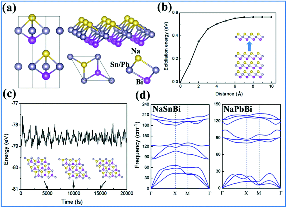 | ||
| Fig. 1 (a) Top view and side view of 2D NaXBi (X = Sn/Pb), (b) cleavage energy of NaSnBi, (c) snapshots of atomic configurations of NaSnBi at the end of MD simulations at 5, 10 and 15 ps at a temperature of 300 K, respectively. (d) Calculated phonon spectrum dispersions of monolayers NaSnBi (left) and NaPbBi (right). | ||
| Structure | NaSnAs | NaSnBi | NaPbBi |
|---|---|---|---|
| 2D | 4.05 | 4.58 | 4.79 |
| 3D | 4.00 | 4.50 | 4.67 |
Now, we examine the possibility of using an exfoliation process to obtain 2D films from the bulk form. We constructed bulk NaSnBi with an optimized lattice a = 4.58 Å and c = 11.71 Å, and then implemented a fracture in the bulk after periodic NaSnBi layers and systematically increased the layered distance. At the end, we calculated the corresponding cleavage energy (CE), as shown in Fig. 1(b). This method is very effective and has been widely confirmed.37 Here, the electric dipole correction55,56 term was used in these calculations. The CE was found to be 0.51 J m−2, which is slightly larger than that of graphite (0.39 J m−2). This can be attributed to ionic interactions in the bulk forming with quite a small distance.
While studying a new material theoretically, it is essential to check whether it is dynamically and mechanically stable. In order to examine the structural stability, we calculated the phonon spectrum dispersion. Note that any structural instability would show up as soft phonon modes with imaginary frequencies. As expected, and shown in Fig. 1(d), all phonon branches have real frequencies throughout the whole Brillouin zone for NaSnBi, confirming its dynamic structural stability. On the other hand, we examined the thermal stability using ab initio molecular dynamics (MD) simulations. As expected from the data shown in Fig. 1(c), the structure of NaSnBi does not collapse during a 20 ps MD simulation, indicating that the melting point of NaSnBi is probably at 300 K. These results reveal that NaSnBi has good thermal stability and can maintain its structural integrity in a high-temperature environment.
The mechanical stability of this structure has been checked by calculating two independent elastic constants expressed as,
 | (2) |
| YS = (c112 − c122)/c11 | (3) |
For NaSnBi and NaPbBi, YS = 178 N m−1 and 152 N m−1, respectively. This is about 40% that of graphene (341 N m−1), one of the strongest materials. Thus, it can be assumed that these systems can stably keep their free-standing structures.
Now we turn to the electronic properties of 2D NaXBi (X = Sn/Pb) films. Fig. 2 displays the calculated band structures for both NaSnBi and NaPbBi films, in which the red, green, and blue dots represent the Bi-pxy, pz, and s states, respectively. In the absence of SOC, both NaSnBi and NaPbBi films exhibit a direct semiconducting character with the valence band maximum (VBM) and conduction band minimum (CBM) degenerate at the Γ point. However, with an increasing atomic number of X, the band gaps decrease drastically, reaching 65 meV for NbPbBi. When switching SOC on, the band gap at the Γ point still exists, but the CBM moves from Γ to the Γ–M line, indicating a transition from a direct to an indirect gap semiconductor.
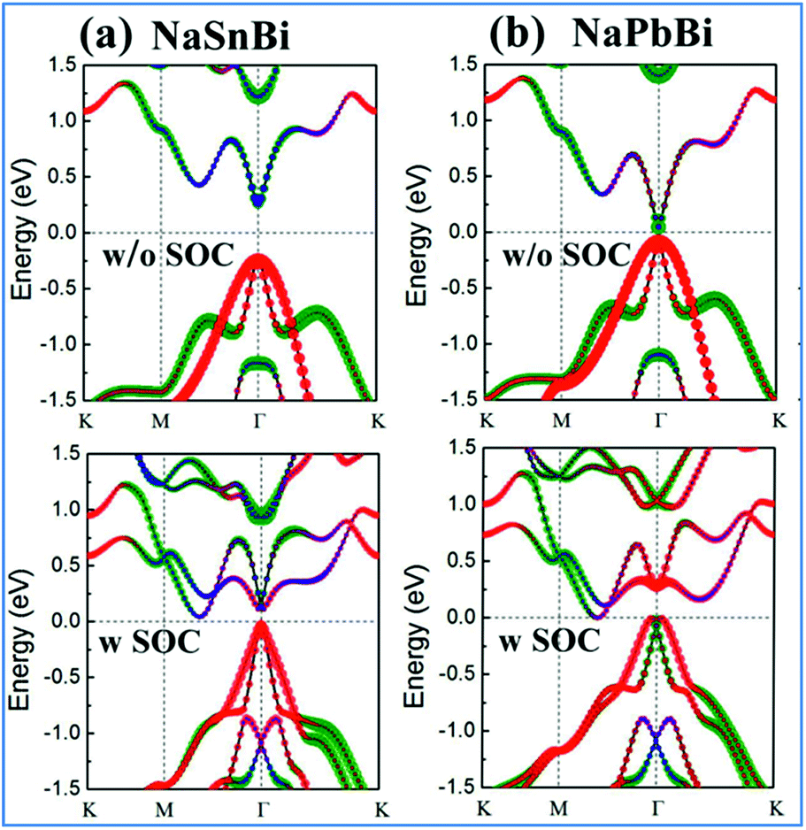 | ||
| Fig. 2 Orbital-resolved band structures of (a) NaSnBi, and (b) NaPbBi without SOC and with SOC, respectively. The red, green, and blue dots are mainly contributed by the pxy, pz, and s orbitals from Bi atoms. | ||
More interestingly, when comparing the band structures of NaSnBi and NaPbBi films to each other, the change trends of the orbital components at the CBM and VBM are different. For NaSnBi, the band character of the CBM and VBM is not influenced by whether the SOC is turned on. Meanwhile for NaPbBi, including SOC makes the components of the CBM and VBM at the Γ point exchange, i.e., the CBM, which is mainly composed of the pz orbital, is pushed downward, while the VBM, which is composed of the px,y orbital (i.e., the hybridized px and py orbitals), is conversely pushed upward. The strong SOC strength from the Bi and Pb atoms makes the band order around the Γ point invert, which is opposite to the band structure alignment without SOC. This px,y–pz band inversion strongly suggests the topologically non-trivial feature of 2D NaPbBi. To overcome the underestimation of the band gap, we further employed HSE06 to check the band gap, see Fig. 6(b). Note that the non-trivial gap at the Fermi level is enlarged from 0.35 eV to 0.42 eV, which is larger than those of Bi (111) (0.2 eV)30 and stanene (0.1 eV).13 This satisfactory bulk gap guarantees its experimental realization and viable applications working at room temperature.
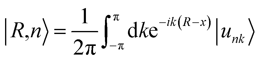
One prominent feature of 2D topological materials is the appearance of topologically protected metallic edge states. To see QSHE explicitly, we calculated the edge Green’s functions of a semi-infinite nanoribbon using an ab initio tight-binding (TB) model with the recursive method based on maximally localized Wannier functions (MLWFs).58 Fig. 3(a) displays the results from fitted DFT and TB model bands, as well as local density of states (LDOS) on the edge states. Note that a pair of gapless edge states traverse across the bulk gap and connect the conduction and valence bands in NaPbBi. By projecting the contribution of spin up and spin down components, we find that the spin-momenta of edge states are spin-momentum locked, which is consistent with band structure results. In fact, the non-trivial topological phase of this structure can be examined using the Z2 invariant by tracing the Wannier Center of Charges (WCCs) using the non-Abelian Berry connection.59 The Wannier functions (WFs) related to the lattice vector R can be written as:
 | (4) |
 can be defined as the mean value of 〈0n|
![[X with combining circumflex]](https://www.rsc.org/images/entities/i_char_0058_0302.gif) |0n〉, where is the position operator and |0n〉 is the state corresponding to a WF in the cell with R = 0. Then we can obtain
|0n〉, where is the position operator and |0n〉 is the state corresponding to a WF in the cell with R = 0. Then we can obtain
 | (5) |
 with S= I or II, where summation in α represents the occupied states and A is the Berry connection. So we have the format of the Z2 invariant:
 | (6) |
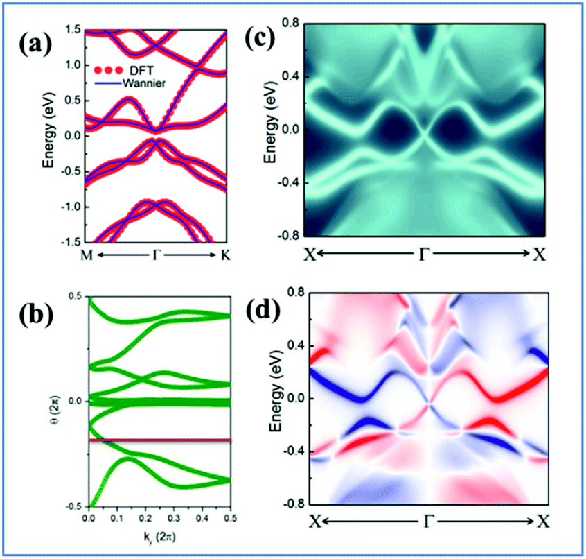 | ||
| Fig. 3 (a) Comparison of band structures under 4% strain of DFT (red circles) and Wannier function (blue lines) methods. (b) Evolution of Wannier centers along ky. The evolution lines cross the arbitrary reference line (red dashed line parallel to ky) an odd number of times. (c) and (d) Topological edge states of NaPbBi under 4% strain obtained from the ab initio TB Wannier function method. | ||
The Z2 invariant can be obtained by counting the even or odd number of crossings of any arbitrary horizontal reference line. Fig. 3(b) gives the evolution lines of WCCs, in which the WCCs evolution curves cross an arbitrary reference line an odd number of times, yielding Z2 = 1, in agreement with the spin-polarized edge states. In this case, the Fermi velocity vF of the edge states was calculated to be 2.6 × 10⁵ m s−1, which is comparable to that of HgTe/CdTe QW,29,30 indicating that the counter-propagating edge states are indeed promising in experiments.
To better understand the band evolution process, we propose a brief schematic of atomic orbitals to interpret the band structure at the Γ point, as shown in Fig. 4. Considering that the states near the Fermi level are mainly from p orbitals, we neglected the effects of other orbitals, and summarized in three stages (I), (II), and (III). In stage (I) the film’s field makes the p orbitals near the Fermi level split into px,y and pz orbitals, due to the threefold axis symmetry, with pz shifting downward with respect to degenerate px,y orbitals. When considering the effects of chemical bonding in stage (II), both px,y and pz states split into the bonding and anti-bonding states, i.e., px,y+ and px,y−, as well as pz+ and pz−. If SOC is turned on, the strong SOC drives the exchange of pz− and px,y+ states at the Fermi level, leading to a clear band inversion, as illustrated in stage (III). Note that this mechanism is different from that seen in graphene,16,17 arsenene60 and Nb2O3 monolayers61 where the SOC does not change the band order, instead only opening a sizable gap at the Fermi level.
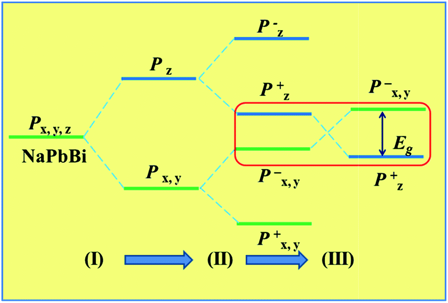 | ||
| Fig. 4 Schematic diagram of the evolution from atomic pz and px,y orbitals into conduction and valence bands at the Γ point in NaPbBi. | ||
Strain has been widely used in 2D materials to modulate their electronic and magnetic properties. Remarkably, non-trivial topological properties and phase transitions in 2D materials are generally sensitive to the lattice parameters. Thus, we explored how the electronic properties of this structure can be engineered using in-plane strain, since it is quite crucial to check the robustness of the topological phase against strain. Here, the strains can be expressed as ε = (a − a0)/a0 along the xy direction, where a0 is the lattice constant of NaPbBi at the ground state. Fig. 5(b) displays the change trend of the band gap and topological phase transition with respect to strains. Note that the non-trivial topology is sensitive to applied strain, ε, upon which the topological phase transition can be tuned efficiently. When under strain ranging from −4 to 12%, NaPbBi undergoes several topological phase transitions in the sequence: non-trivial topological semi-metal phase (<−1%) → non-trivial topological insulating phase (0–6.8%) → trivial (normal) insulating phase (>7.0%). Obviously, the tunable range of the non-trivial topological phase is in the range of −4% to 7%. The band structures with various applied strains are shown in Fig. 6(a). Such a strain induced topological phase transition in this structure greatly expands the potential use of NaPbBi in electronics and spintronics, and the tunability of the non-trivial band gap offers a promising route to engineering the topology using biaxial strain for the benefit of nanoelectronics.
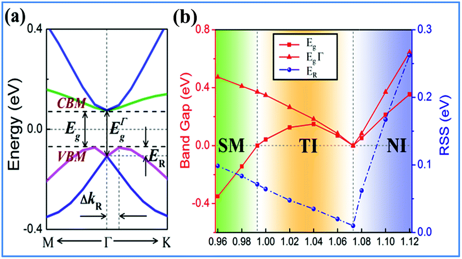 | ||
| Fig. 5 (a) The calculated Rashba SOC of 2D NaPbBi, (b) the variations of the global band gap Eg, band gap at the Γ point and RSS ER as a function of external strain for NaPbBi. | ||
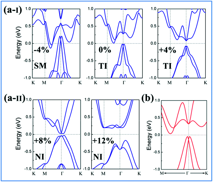 | ||
| Fig. 6 (a-I) and (a-II) Calculated PBE band structures (blue line) of NaPbBi under strains of −4, 0, +4, +8, +12%, respectively. (b) The band structures with HSE06 (red line) of the NaPbBi crystal. | ||
Another prominent feature is Rashba SOC related to spin topology, unlike the systems with spatial inversion-symmetry. Fig. 5(a) displays the spin–orbit split momentum distribution that accompanies the antiparallel spin direction, indicating that the band splitting at the Γ point is Rashba-type. To give a better understanding of Rashba SOC splitting, we present the spin texture in the highest valence bands for NaPbBi in Fig. 7, where the spin components projected to the in-plane polarization are normal to k in the Brillouin zone. The RSS is characterized by the Rashba energy ER and corresponding momentum offset ΔkR away from the crossing point, which is illustrated in Fig. 5(a). From an estimation of ΔkR and a fitting value of the effective mass, we found that the effective Rashba constant 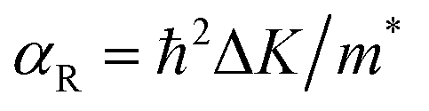 reaches a value as large as 0.18 eV Å−1, larger than the results for InGaAs/GaAs quantum dots (αR ∼ 0.08 − 0.12 eV Å−1), or InGaAs/InAlAs quantum wells (αR = 0.07 eV Å−1).62 More interestingly, the Rashba energy ER is tunable to a great extent by external in-plane strains. NaPbBi has an extremely large ER = 71 meV under 1% pressure. The larger RSS of the electronic bands obtained here provides a chance for spintronic device applications without the magnetic field, for instance, in a spin field-effect transistor (FET). More interestingly, when moving around the Fermi surface, the spin orientation rotates simultaneously, forming a right-handed spin–orbit ring, which indicates the bulk non-trivial topology. Because the surface is very close to the Fermi level, it may be detected in future ARPES experiments.
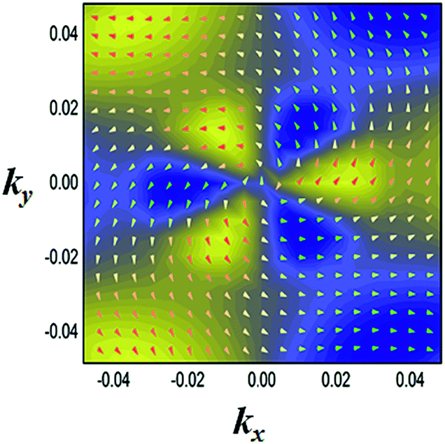 | ||
| Fig. 7 Spin texture in the highest valence bands for the NaBiPb monolayer. Arrows refer to the in-plane orientation of the spins, and the background color denotes the z component of the spins. | ||
To give a better understanding of the topological phase transition mechanism between the p orbits, we constructed an effective tight-binding (TB) model on the basis of |px, py, pz〉 and the second quantized representation can be expressed as
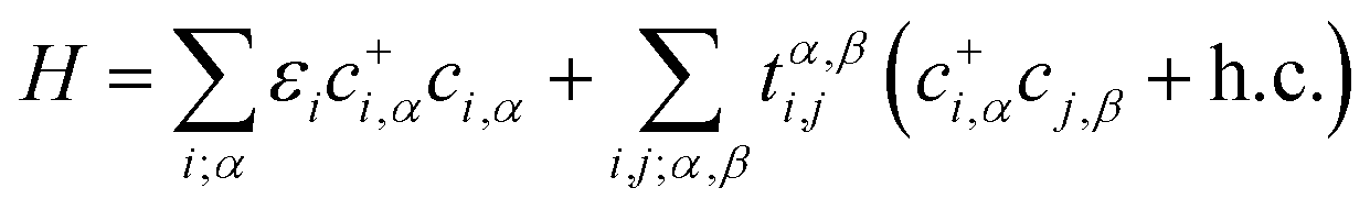 | (7) |
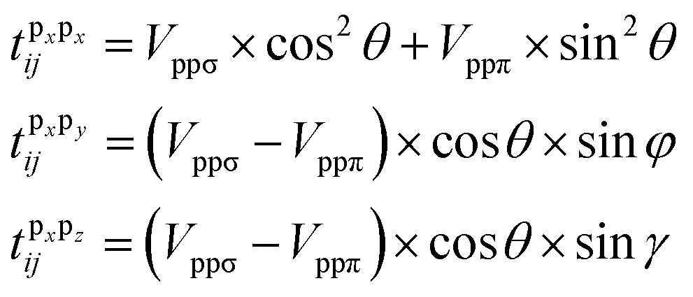 | (8) |
To evaluate the effect of SOC in our TB calculations, we further considered an on-site term, expressed as
HSOC = λ〈![[L with combining right harpoon above (vector)]](https://www.rsc.org/images/entities/i_char_004c_20d1.gif) · ·![[small sigma, Greek, vector]](https://www.rsc.org/images/entities/char_e1c9.gif) 〉αβ 〉αβ |
is the Pauli matrix, and λ is the SOC strength of this structure. Our calculated results show that increasing SOC strength, λ, initially reduces the band gap at the Γ point, which is consistent with the results of the DFT calculations. When λ reaches 0.57 eV, the valence and conduction bands meet at a single point, at the Γ point, resulting in complete band-gap closure. Increasing λ further reopens the band gap and eventually produces a non-trivial band structure. Obviously, it is the SOC effect that leads to a trivial–non-trivial topological phase transition.
Tuning the electronic properties of 2D materials is crucial for their applications in opto-electronic and spintronic devices. Heterostructures have been widely used in conventional semiconductors for achieving versatile electronic properties. For the development of future 2D materials, van der Waals (vdW) heterostructures have been recognized as among the most promising candidates and field-effect transistors and memory cells made of TMD/graphene heterostructures have been reported.64,65 Additionally, the topological properties of germanene on MoS2 and those of stanene on InSe, Ge(111), and H-passivated SiC have been reported.66,67 To utilize the non-trivial topological properties of the 2D NaPbBi in the honeycomb structure, we selected 3 × 3 MoS2 as a substrate to construct a NaPbBi/MoS2 heterostructure (HTS), as illustrated in Fig. 8(a) and (b).68,69 After careful structural optimization, the distance (d) between adjacent layers is 3.782 Å, with the binding energy being −0.71 eV, suggesting a typical vdW HTS. Fig. 8(c) displays the corresponding band structures with and without SOC, respectively. Note that a few bands appear within the bulk gap of the MoS2 substrate around the Fermi level, which is mainly contributed by NaPbBi according to wave-function analysis. By projecting Bloch wave functions onto the atomic orbitals of 2D NaPbBi, Bloch states contributed by the pxy and pz orbitals are visualized by blue and red dots, respectively. Obviously, this SOC-induced band gap is topologically non-trivial as illustrated by the band inversion, thus NaPbBi is a robust 2D TI supported on a MoS2 substrate.
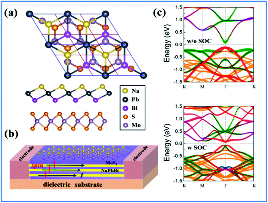 | ||
| Fig. 8 (a) Top and side view of the crystal structure of the NaPbBi/MoS2 heterostructure, with the supercell of 2 × 2 NaPbBi on the 3 × 3 MoS2 substrate, which matches well. (b) Schematic model of NaPbBi/MoS2 HTS for quantum state measurement. Vertical arrows show the spin orientation of electrons in the edge states and horizontal arrows show their transport directions. (c) The band structure without and with SOC in which the red, green, and blue dots represent pxy, pz, and s states, respectively, while yellow dots represent the MoS2 substrate effect. | ||
4. Conclusions
Based on first-principles calculations, we propose new 2D NaXBi (X = Sn/Pb) films, which can be exfoliated from their bulk NaXBi forms. The phonon spectra and ab initio molecular dynamic simulations show that both films have high thermodynamic stability and their 2D lattices can be retained at temperatures up to 300 K. The spin-polarized calculations indicate that 2D NaSnBi is a trivial insulator in its ground state, while NaPbBi turns into a 2D TI with a gap as large as 0.35 eV at the Γ point, which is important for the practical realization of QSHE working at room temperature. The non-trivial band topology, induced via pxy–pz band inversion, is confirmed by the calculated Z2 index and helical edge states. Unlike 2D Bi(111) or BiX (X = H, F, Cl) films, the inversion-symmetry breaking in these films gives rise to a sizable Rashba splitting energy of 64 meV, which can further be engineered in a range of strains (−1 to 7%). Our work provides new strategies to obtain desired 2D films for spintronic devices at room temperature.Conflicts of interest
There are no conflicts to declare.Acknowledgements
This work was supported by the Natural Science Foundation of Shandong Province under Grant No ZR2018MA033, and the National Natural Science Foundation of China under Grant No 61571210.References
- K. S. Novoselov, A. K. Geim, S. V. Morozov, D. Jiang, Y. Zhang, S. V. Dubonos, I. V. Grigorieva and A. A. Firsov, Science, 2004, 306, 666–669 CrossRef PubMed.
- X. Qian, J. Liu, L. Fu and J. Li, Science, 2014, 346, 1344 CrossRef PubMed.
- K. F. Mak, C. Lee, J. Hone, J. Shan and T. F. Heinz, Phys. Rev. Lett., 2010, 105, 136805–R CrossRef PubMed.
- A. Splendiani, L. Sun, Y. Zhang, T. Li, J. Kim, C. Y. Chim, G. Galli and F. Wang, Nano Lett., 2010, 10, 1271–1275 CrossRef PubMed.
- H. Liu, A. T. Neal, Z. Zhu, Z. Luo, X. Xu, D. Tománek and P. D. Ye, ACS Nano, 2014, 8, 4033–4041 CrossRef PubMed.
- L. Li, Y. Yu, G. J. Ye, Q. Ge, X. Ou, H. Wu, D. Feng, X. H. Chen and Y. Zhang, Nat. Nanotechnol., 2014, 9, 372–377 CrossRef PubMed.
- M. E. Davila, L. Xian, S. Cahangirov, A. Rubio and G. L. Lay, New J. Phys., 2014, 16, 3579–3587 CrossRef.
- S. Cahangirov, M. Topsakal, E. Aktürk, H. Şahin and S. Ciraci, Phys. Rev. Lett., 2009, 102, 236804 CrossRef PubMed.
- C. W. Z. Zhang and S. S. Yan, J. Phys. Chem. C, 2012, 116, 4163–4166 CrossRef.
- A. J. Mannix, X. F. Zhou, B. Kiraly, J. D. Wood, D. Alducin, B. D. Myers, X. Liu, B. L. Fisher, U. Santiago, J. R. Guest, M. J. Yacaman, A. Ponce, A. R. Oganov, M. C. Hersam and N. P. Guisinger, Science, 2015, 350, 1513–1516 CrossRef PubMed.
- F. B. Zheng and C. W. Zhang, Nanoscale Res. Lett., 2012, 7, 422 CrossRef PubMed.
- N. Ullah, R. Q. Zhang, G. Murtaza, A. Yar and A. Mahmood, Solid State Commun., 2016, 246, 54–58 CrossRef.
- R. W. Zhang, C. W. Zhang, W. X. Ji, S. S. Li, S. J. Hu, S. S. Yan, P. Li, P. J. Wang and F. Li, New J. Phys., 2015, 17, 083036 CrossRef.
- M. Z. Hasan and C. L. Kane, Rev. Mod. Phys., 2010, 82, 3045–3067 CrossRef.
- J. E. Moore, Nat. Nanotechnol., 2013, 8, 194–198 Search PubMed.
- C. L. Kane and E. J. Mele, Phys. Rev. Lett., 2005, 95, 226801 CrossRef PubMed.
- C. L. Kane and E. J. Mele, Phys. Rev. Lett., 2005, 95, 146802 CrossRef PubMed.
- Z. Fei, T. Palomaki, S. Wu, W. Zhao, X. Cai, B. Sun, P. Nguyen, J. Finney, X. Xu and D. H. Cobden, Nat. Phys., 2017, 13, 677 Search PubMed.
- S. Wu, V. Quinn, D. Gibson, K. Watanabe, T. Taniguchi, R. J. Cava, P. Jarillo-Herrero, 2017, 03584, arXiv: 1711.
- S. Tang, C. Zhang, D. Wong, Z. Pedramrazi, H. Tsai, C. Jia, B. Moritz, M. Claassen, H. Ryu, S. Kahn, J. Jiang, H. Yan, M. Hashimoto, D. Lu, R. Moore, C. Hwang, C. Hwang, Z. Hussain, Y. Chen, M. Ugeda, Z. Liu, X. Xie, T. Devereaux and M. Crommie, Nat. Phys., 2017, 13, 683–687 Search PubMed.
- Z. Jia, Y. Song, X. Li, K. Ran, P. Lu, H. Zheng, X. Zhu, Z. Shi, J. Sun, J. Wen, D. Xing and S. Li, Phys. Rev. B, 2017, 96, 041108 CrossRef.
- L. Peng, Y. Yuan, G. Li, X. Yang, J. Xian, C. Yi, Y. Shi and Y. Fu, Nat. Commun., 2017, 8, 659 CrossRef PubMed.
- C. C. Liu, W. Feng and Y. Yao, Phys. Rev. Lett., 2011, 107, 076802 CrossRef PubMed.
- R. W. Zhang, C. W. Zhang, W. X. Ji, P. Li, P. J. Wang, S. S. Li and S. S. Yan, Appl. Phys. Lett., 2016, 109, 182109 CrossRef.
- C. C. Liu, H. Jiang and Y. Yao, Phys. Rev. B, 2011, 84, 4193–4198 Search PubMed.
- R. W. Zhang, W. X. Ji, C. W. Zhang, S. S. Li, P. Li and P. J. Wang, J. Mater. Chem. C, 2016, 4, 2088–2094 RSC.
- Y. Xu, B. Yan, H. J. Zhang, J. Wang, G. Xu, P. Tang, W. H. Duan and S. C. Zhang, Phys. Rev. Lett., 2013, 111, 136804 CrossRef PubMed.
- H. Zhao, C. W. Zhang, W. X. Ji, R. W. Zhang, S. S. Li, S. S. Yan, B. M. Zhang and P. J. Wang, Sci. Rep., 2016, 6, 20152 CrossRef PubMed.
- B. A. Bernevig, T. L. Hughes and S. C. Zhang, Science, 2006, 314, 1757–1761 CrossRef PubMed.
- M. König, S. Wiedmann, C. Brüne, A. Roth, H. Buhmann, L. W. Molenkamp, X. L. Qi and S. C. Zhang, Science, 2007, 318, 766–770 CrossRef PubMed.
- C. Liu, T. L. Hughes, X. L. Qi, K. Wang and S. C. Zhang, Phys. Rev. Lett., 2008, 100, 236601 CrossRef PubMed.
- I. Knez, R. R. Du and G. Sullivan, Phys. Rev. Lett., 2011, 107, 136603 CrossRef PubMed.
- M. Wada, S. Murakami, F. Freimuth and G. Bihlmayer, Phys. Rev. B, 2011, 83, 121310 CrossRef.
- S. S. Li, W. X. Ji, P. Li, S. J. Hu, L. Cai, C. W. Zhang and S. S. Yan, ACS Appl. Mater. Interfaces, 2017, 9, 41443 CrossRef PubMed.
- C. C. Liu, S. Guan, Z. G. Song, S. Y. Yang, J. B. Yang and Y. Yao, Phys. Rev. B, 2014, 90, 085431 CrossRef.
- J. J. Zhou, W. Feng, G. B. Liu and Y. Yao, New J. Phys., 2015, 17(1), 015004 CrossRef.
- C. W. Niu, G. Bihlmayer, H. B. Zhang, D. Wortmann, S. Blügel and Y. Mokrousov, Phys. Rev. B, 2015, 91, 041303 CrossRef.
- R. Zhang, C. Zhang, W. Ji, S. Yan and Y. Yao, Nanoscale, 2017, 9, 8207–8212 RSC.
- S. S. Li, W. X. Ji, P. Li, S. J. Hu, L. Cai, C. W. Zhang and S. S. Yan, ACS Appl. Mater. Interfaces, 2017, 9, 21515 CrossRef PubMed.
- M. Eschbach, M. Lanius and C. W. Niu, et al., Nat. Commun., 2017, 8, 14976 CrossRef PubMed.
- C. C. Liu, J. J. Zhou, Y. Yao and F. Zhang, Phys. Rev. Lett., 2016, 116(6), 066801 CrossRef PubMed.
- F. C. Chuang, L. Z. Yao, Z. Q. Huang, Y. T. Liu, C. H. Hsu, T. Das, H. Lin and A. Bansil, Nano Lett., 2014, 14, 2505–2508 CrossRef PubMed.
- L. Li, X. Zhang, X. Chen and M. Zhao, Nano Lett., 2015, 15, 1296–1301 CrossRef PubMed.
- I. K. Drozdov, A. Alexandradinata, S. Jeon, S. Nadj-Perge, H. Ji, R. J. Cava, B. A. Bernevig and A. Yazdani, Nat. Phys., 2014, 10(9), 664 Search PubMed.
- L. Miao, M. Y. Yao, W. Ming, F. Zhu, C. Q. Han, Z. F. Wang, D. D. Guan, C. L. Gao, C. H. Liu, F. Liu and D. Qian, Phys. Rev. B, 2015, 91, 205414 CrossRef.
- F. Reis, G. Li, L. Dudy, M. Bauernfeind, S. Glass, W. Hanke, R. Thomale, J. Schäfer and R. Claessen, Science, 2017, 357, 287 CrossRef PubMed.
- G. Kresse and J. Furthmüller, Phys. Rev. B, 1996, 54(16), 11169 CrossRef.
- G. Kresse and J. Hafner, Phys. Rev. B, 1994, 49(20), 14251 CrossRef.
- G. Kresse and D. Joubert, Phys. Rev. B, 1999, 59(3), 1758 CrossRef.
- J. P. Perdew and Y. Wang, Phys. Rev. B, 1992, 45(23), 13244 CrossRef.
- J. Heyd, G. E. Scuseria and M. Ernzerhof, J. Chem. Phys., 2006, 124, 219906 CrossRef.
- A. Togo, F. Oba and I. Tanaka, Phys. Rev. B, 2008, 78, 134106 CrossRef.
- Z. Lin, G. Wang, C. Le, H. Zhao, N. Liu, J. Hu, L. Guo and X. Chen, Phys. Rev. B, 2017, 95, 165201 CrossRef.
- X. Dai, C. C. Le, X. X. Wu, S. S. Qin, Z. P. Lin and J. P. Hu, Chin. Phys. Lett., 2016, 33(12), 127301 CrossRef.
- G. Makov and M. C. Payne, Phys. Rev. B, 1995, 51, 4014 CrossRef.
- J. Neugebauer and M. Scheffler, Phys. Rev. B, 1992, 46(24), 16067 CrossRef.
- M. P. L. Sancho, J. M. L. Sancho and J. Rubio, J. Phys. F: Met. Phys., 1984, 14, 1205 CrossRef.
- A. A. Soluyanov and D. Vanderbilt, Phys. Rev. B, 2011, 83, 235401 CrossRef.
- R. Yu, X. L. Qi, A. Bernevig, Z. Fang and X. Dai, Phys. Rev. B, 2011, 84, 075119 CrossRef.
- Y. P. Wang, W. X. Ji, C. W. Zhang, P. Li, S. F. Zhang, P. J. Wang, S. S. Li and S. S. Yan, Appl. Phys. Lett., 2017, 110, 213101 CrossRef.
- S. J. Zhang, C. W. Zhang, S. F. Zhang, W. X. Ji, P. Li, P. J. Wang, S. S. Li and S. S. Yan, Phys. Rev. B, 2017, 96, 205433 CrossRef.
- J. Nitta, T. Akazaki, H. Takayanagi and T. Enoki, Phys. Rev. Lett., 1997, 78, 1335 CrossRef.
- B. Yan and S. C. Zhang, Rep. Prog. Phys., 2012, 75, 096501 CrossRef PubMed.
- S. Bertolazzi, D. Krasnozhon and A. Kis, ACS Nano, 2013, 7, 3246–3252 CrossRef PubMed.
- T. Georgiou, R. Jalil, B. D. Belle, L. Britnell, R. V. Gorbachev, S. V. Morozov, Y.-J. Kim, A. Gholinia, S. J. Haigh and O. Makarovsky, Nat. Nanotechnol., 2012, 8, 100 CrossRef PubMed.
- Y. P. Wang, W. X. Ji, C. W. Zhang, P. Li, P. J. Wang, B. Kong, S. S. Li, S. S. Yan and K. Liang, Appl. Phys. Lett., 2017, 110, 233107 CrossRef.
- Y. Fang, Z.-Q. Huang, C.-H. Hsu, X. Li, Y. Xu, Y. Zhou, S. Wu, F.-C. Chuang and Z.-Z. Zhu, Sci. Rep., 2015, 5, 14196 CrossRef PubMed.
- L. Zhang, P. Bampoulis, A. N. Rudenko, Q. Yao, A. van Houselt, B. Poelsema, M. I. Katsnelson and H. J. W. Zandvliet, Phys. Rev. Lett., 2016, 116, 256804 CrossRef PubMed.
- B. Cho, J. Yoon, S. K. Lim, A. Kim, D. Kim, S. Park, J. Kwon, Y. Lee, K. Lee, B. H. Lee, H. C. Ko and M. G. Hahm, ACS Appl. Mater. Interfaces, 2015, 7, 16775–16780 CrossRef PubMed.
| This journal is © The Royal Society of Chemistry 2018 |