
 Open Access Article
 This Open Access Article is licensed under a Creative Commons Attribution-Non Commercial 3.0 Unported Licence
Improvement of thermoelectric performance of copper-deficient compounds Cu2.5+δIn4.5Te8 (δ = 0–0.15) due to a degenerate impurity band and ultralow lattice thermal conductivity†
Ting Renab,
Pengzhan Ying*a,
Gemei Cai c,
Xiaoyan Lid,
Zhongkang Han*d,
Lei Minab and
Jiaolin Cui*b
c,
Xiaoyan Lid,
Zhongkang Han*d,
Lei Minab and
Jiaolin Cui*b
aMaterials Science and Engineering College, China University of Mining and Technology, Xuzhou 221116, China. E-mail: ypz3889@sina.com
bSchool of Materials & Chemical Engineering, Ningbo University of Technology, Ningbo 315016, China. E-mail: cuijiaolin@163.com
cSchool of Materials Science and Engineering, Central South University, Changsha 410083, China
dDivision of Interfacial Water and Key Laboratory of Interfacial Physics and Technology, Shanghai Institute of Applied Physics, Chinese Academy of Sciences, Shanghai, 201800, China. E-mail: hegongdahuagong@126.com
First published on 31st July 2018
Abstract
Cu–In–Te ternary chalcogenides have unique crystal and band structures; hence they have received much attention in thermoelectrics. In this work we have observed an enhancement in Hall carrier concentration (nH) and ultralow lattice thermal conductivity (κL) when Cu was added to ternary Cu2.5+δIn4.5Te8 (δ = 0–0.15) compounds. The enhancement in nH is attributed to a degenerate impurity band at the G point in the valence band maximum (VBM), while the extremely low κL results from the increased lattice disorder. We thus obtained the minimum κL value of only 0.23 W K−1 m−1 in the sample at δ = 0.1 and 820 K, which is in good agreement with the calculation using the Callaway model. The highest thermoelectric figure of merit ZT is 0.84 for the material at δ = 0.1, which is about 0.38 higher than that of the pristine Cu2.5In4.5Te8.
1. Introduction
Thermoelectric (TE) materials have become increasingly important due to their potential usage in TE devices. However, the efficiency of current TE devices, which is strongly dependent on the TE figure of merit (ZT), ZT = Tα2σ/(κe + κL), is still low, because it is hard to tune the three parameters (α, σ and κe) separately, as they are interdependent on each other. Here α, σ, κe and κL are the Seebeck coefficient, electrical conductivity, electronic and lattice thermal conductivities, respectively. In order to improve the TE performance of materials, many pioneering works have been done, such as nano and band structure engineering,1–4 phonon liquid and electronic crystal (PLEC) concept applications,5,6 and magnetoelectric interaction exploration.7,8 Although these approaches did improve the power factor (α2σ) or reduce the lattice part (κL) provided that the carrier concentration is optimized,9 it is still necessary to develop new materials.Cu–In–Te ternary chalcogenides, such as, CuInTe2,10–13 Cu2In4Te7,14 Cu3In5Te9 (ref. 15 and 16) and Cu3In7Te12,17 present potential TE performance, and we have observed the highest ZT value of 1.24 in Ag-added CuInTe2.18 Inspired by controllable crystal or band structure and reducible lattice thermal conductivity in Cu–In–Te chalcogenides,19,20 as those observed in Cu(Ag)–Ga–Te materials,21,22 it is believed that, through tuning carrier concentration and/or blocking of phonon transport,23,24 we can also engineer the TE performance of copper deficient Cu–In–Te compounds.
In this work, we have investigated the structures and TE performance of Cu-deficient ternary chalcogenide Cu2.5In4.5Te8-based compounds. By adding extra Cu, we successfully improved the TE performance. The mechanism behind this significant improvement is the degenerate impurity band in the VBM and a decrease in lattice thermal conductivity caused by increased lattice disorder in the structure. In the end, we obtained the highest ZT value of 0.84, which is about 0.36 higher than that of pristine Cu2.5In4.5Te8.
2. Experimental
2.1 Sample preparation
The mixtures of three elements Cu, In and Te, with a purity of more than 99.999% (Emei Semicon. Mater. Co., Ltd. Sichuan, CN), were loaded into different silica vacuum tubes according to the formula Cu2.5+δIn4.5Te8 (δ = 0, 0.05, 0.1, 0.15, 0.2) They were then heated to 1123 K within 4.5 h and held at this temperature for 24 h followed by annealing at 796 K for 72 h. During the melting process, the samples were rocked for 30 s every 1 h to ensure a homogeneous composition without segregation. After cooling down to the room temperature (RT), the ingots were ball milled for 5 h at a rotation rate of 350 rpm for 5 h in stainless steel bowls that contained benzinum. The dried powders were then rapidly sintered using spark plasma sintering apparatus (SPS-1030) at a peak temperature of ∼900 K and a pressure of 50 MPa. The densities (d) of the polished bulks, which have more than 95% theoretical density, were measured using Archimedes' method.The bulk samples with sizes of about 2.5 × 3 × 12 mm3 and 2 × 2 × 7 mm3 were prepared for electrical property and Hall coefficient measurements respectively, and those of ϕ 10 × 1.5 mm2 for thermal diffusivity measurement.
2.2 Physical property measurements
Both the Seebeck coefficients (α) and electrical conductivities (σ) were measured simultaneously under a helium atmosphere from RT to ∼820 K in a ULVAC ZEM-3 instrument system with an uncertainty of <6.0% for each. The thermal conductivities were calculated based on the equation κ = dλCp, where the thermal diffusivities (λ) were measured by TC-1200RH instrument in a vacuum with an uncertainty of <10.0%. The Dulong–Petit rule is used to estimate the heat capacities (Cp) above RT. The three physical parameters (α, σ, κ) were finalized by taking the average values of several samples tested by the same method. The lattice contribution (κL) was the total κ minus the electronic contribution (κe). Here κe is expressed by the Wiedemann–Franz (W–F) relation, κe = L0σT, where L0 is the Lorenz number, estimated using the formula L0 = 1.5 + exp(−|α|/116)25 (where L0 is in 10 × −8 WΩ K−2 and |α| in μV K−1). The TE figure of merits (ZTs) were calculated using the three parameters above according to the equation, ZT = Tα2σ/κ, with the total uncertainty of about 20%.Hall coefficients (RH) were measured by using a four-probe configuration in a system (PPMS, Model-9) with a magnetic field up to ± 5 T. The Hall mobility (μ) and carrier concentration (nH) were calculated according to the relations μ = |RH|σ and nH = 1/(e RH) respectively, where e is the electron charge.
2.3 Structural, thermal analyses and first-principles calculations
The structural analysis of the powders was made by powder X-ray diffractometer (D8 Advance) operating at 50 kV and 40 mA at Cu Kα radiation (λ = 0.15406 nm) in the range from 10° to 110° with a step size of 0.02°, and a X'Pert Pro, PANalytical code was used to do the Rietveld refinement of XRD patterns of the titled compounds. The lattice constants a and c were directly obtained from the refinement of the XRD patterns using Jade software.Differential scanning calorimeter (DSC) and thermogravimetry (TG) were conducted in a Netzch STA 449 F3 Jupiter equipped with a TASC414/4 controller. The instrument was calibrated from a standard list. The sample of the powder (δ = 0) was loaded into an open alumina crucible. The measurement was performed after the samples were heated up to ∼850 K and then cooled down to 303 K with a heating/cooling rate of 5 K min−1 in Ar atmosphere.
The first-principles calculations were carried out using spin-polarized DFT with generalized gradient approximation (GGA) of Perdew–Burke–Ernzerhof (PBE) implemented in VASP code.26,27 We used the DFT+U methodology with a value of U = 5.0 eV in this work.28 The valence electronic states were expanded in the basis of plane waves, and the core–valence interaction is represented using the scalar relativistic projector augmented wave (PAW)29 approach and a cutoff of 400 eV. More accurate single point electronic structure calculations were further performed using HSE06 functional to obtain the band structures and the density of states (DOS) of Cu28+yIn33Te64 (y = 1–3) system.
3. Results and discussions
3.1 Composition analysis and XRD refinements
Fig. S1† shows the EMPA mappings of three elements Cu, In and Te for the sample at δ = 0.1. The average chemical compositions of Cu2.5In4.5Te8 (δ = 0) and Cu2.6In4.5Te8 (δ = 0.1) are shown in Table S1,† where the number of Te is normalized to 8.0 (the actual moles of Te are slightly less than nominal ones). In this case, the normalized moles of Cu (2.53–2.62) and In (4.51–4.53) are a little higher than nominal ones. This suggests that there is a subtle deficiency in Te, which is mainly ascribed to the measurement uncertainty. Besides, there are Cu-rich areas inside the matrix, indicating that the three elements are not distributed perfectly.We used XRD data to conduct the Rietveld refinement, and the refined XRD patterns of four compounds Cu2.5+δIn4.5Te8 (δ = 0, 0.05, 0.1, 0.15) are shown in Fig. S2.† We found that the nominal compounds Cu2.5+δIn4.5Te8 (δ = 0, 0.05, 0.1, 0.15) crystallize in a crystal structure of CuInTe2 (PDF 65-0245, s. g.: I-42d (no.122)), and the real refined compositions are Cu3.52In4.16Te8 (δ = 0), Cu3.59In4.16Te8 (δ = 0.05), Cu3.66In4.16Te8 (δ = 0.1), Cu3.73In4.16Te8 (δ = 0.15), respectively. It is highly possible that the refined compositions would deviate from nominal ones, and we believe the reason behind that is the precipitation of trace impurity phases, as some elements are insoluble in their own phases. It is hard to identify the few secondary phases because of the low accuracy of XRD analysis. The XRD patterns of the powders are shown in Fig. S3,† where the indices of crystallographic planes are specified according to those of CuInTe2 (PDF: 65-0245).
From the refinements, the lattice constants a (6.1800–6.1830) and c (12.366–12.379) vary slightly with the extra Cu content (δ value). The refined a and c values are shown in Table 1, where the structural variables RB (Bragg factor), Rp (profile factor), Rwp (weighted profile factor), and S (goodness of fit indicator), are in the range of 7.01–7.80%, 4.75–5.64%, 5.71–6.98%, and 1.63–2.03 respectively. Table 2 presents the Wyckoff positions, atomic coordinates and SOFs (site of occupation factors). The SOF values indicate that the element Cu totally resides in Cu4a site with SOFs of 0.8800 (δ = 0), 0.8976 (δ = 0.05), 0.9160 (δ = 0.1), and 0.9328 (δ = 0.15) respectively. Besides, there is a small amount of element In1 that reside at Cu4a site (SOFs = 0.04), and the element In2 and Te reside at In4b site (SOFs = 1) and Te8d site (SOFs = 1) for all samples respectively. This indicates there is a small portion of antisite defect InCu created. This defect acts as a donor and neutralizes the p-type carrier concentration to some extents.
| δ = 0 | δ = 0.05 | δ = 0.1 | δ = 0.15 | |
|---|---|---|---|---|
| Chemical formula | Cu3.52In4.16Te8 | Cu3.59In4.16Te8 | Cu3.66In4.16Te8 | Cu3.73In4.16Te8 |
| Space group | I![[4 with combining macron]](https://www.rsc.org/images/entities/char_0034_0304.gif) 2d (no. 122) 2d (no. 122) |
I2d (no. 122) |
I2d (no. 122) |
I2d (no. 122) |
| Z | 1 | 1 | 1 | 1 |
| a (Å) | 6.1803 (6) | 6.1819 (6) | 6.1800 (5) | 6.1830 (6) |
| b (Å) | 6.1803 (6) | 6.1819 (6) | 6.1800 (5) | 6.1830 (6) |
| c (Å) | 12.366 (2) | 12.370 (2) | 12.375 (1) | 12.379 (2) |
| V (Å3) | 472.32 (9) | 472.7 (1) | 472.61 (8) | 473.3 (1) |
| RB (%) | 7.41 | 7.40 | 7.80 | 7.01 |
| Rp (%) | 5.64 | 5.29 | 5.05 | 4.75 |
| Rwp (%) | 6.98 | 6.53 | 6.32 | 5.71 |
| S | 2.03 | 1.86 | 1.78 | 1.63 |
| Compositions | Atom | Site | x | y | z | Biso (Å2) | Occupancy |
|---|---|---|---|---|---|---|---|
| δ = 0 (Cu3.52In4.16Te8) | Cu | 4a | 0 | 0 | 0 | 1.74(6) | 0.8800 |
| In1 | 4a | 0 | 0 | 0 | 1.74(6) | 0.0400 | |
| In2 | 4b | 0 | 0 | 0.5 | 1.56(3) | 1 | |
| Te | 8d | 0.2234(6) | 0.25 | 0.125 | 1.11(1) | 1 | |
| δ = 0.05 (Cu3.59In4.16Te8) | Cu | 4a | 0 | 0 | 0 | 1.47(6) | 0.8976 |
| In1 | 4a | 0 | 0 | 0 | 1.47(6) | 0.0400 | |
| In2 | 4b | 0 | 0 | 0.5 | 2.49(3) | 1 | |
| Te | 8d | 0.2238(6) | 0.25 | 0.125 | 1.49(1) | 1 | |
| δ = 0.10 (Cu3.66In4.16Te8) | Cu | 4a | 0 | 0 | 0 | 1.52(5) | 0.9160 |
| In1 | 4a | 0 | 0 | 0 | 1.52(5) | 0.0400 | |
| In2 | 4b | 0 | 0 | 0.5 | 2.23(3) | 1 | |
| Te | 8d | 0.2240(4) | 0.25 | 0.125 | 1.28(1) | 1 | |
| δ = 0.15 (Cu3.73In4.16Te8) | Cu | 4a | 0 | 0 | 0 | 1.52(5) | 0.9328 |
| In1 | 4a | 0 | 0 | 0 | 1.52(5) | 0.0400 | |
| In2 | 4b | 0 | 0 | 0.5 | 2.22(3) | 1 | |
| Te | 8d | 0.2248(4) | 0.25 | 0.125 | 1.31(1) | 1 |
3.2 Calculations of band structures
In order to gain a better understanding of the band structures upon the addition of Cu, we have conducted first-principles calculations of Cu28+yIn33Te64 (y = 1–3), assuming that the added Cu atoms reside in the copper vacancy, as shown in Fig. S4.† The band structures and the density of the states (DOS) are shown in Fig. 1, where it shows that the Fermi level (Ef) unpins and gradually moves into the inner side of the conduction band (CB). In addition to that, an impurity band (IB) has formed within a gap (the blue line), which is highly degenerate at G point in the valence band maximum (VBM) as y value increases. However, the IB is very weak in DOS, see the close-up view in Fig. S5.† | ||
| Fig. 1 Band structures of Cu28+yIn33Te64 (y = 0–3) assuming that the extra Cu resides in the Cu vacancy. It was observed that the Fermi level (Ef) unpins and moves into the conduction band (CB) as Cu content increases. In addition to that, an impurity band (IB) (blue line) is formed. This IB is highly degenerate at G point in the valence band maximum (VBM), although IB is very weak in the density of the sates (DOS). | ||
In addition, the formation energies (dH) for the occupation of Cu site by In in the compounds Cu31In33Te64 and Cu32In32Te64 are 2.89 eV, while dH values for the Cu vacancy formation from Cu31In33Te64 to Cu30In33Te64, Cu30In33Te64 to Cu29In33Te64, and Cu29In33Te64 to Cu28In33Te64 are 3.48 eV, 3.65 eV and 3.70 eV respectively. The more the extra Cu content, the less the formation energy of Cu vacancy is. These results indicate that an extra Indium is energetically favorable to the Cu site, while the formation of Cu vacancy is relatively difficult. The results from formation energy calculations are in a good agreement with Rietveld refinement shown in Table 2. The calculated bandgap is, on the contrary, about 0.40–0.48 eV, which slightly fluctuates as the extra Cu content increases.
3.3 Hall carrier concentration and mobility
Upon the occupation of extra Cu in the copper vacancy (VCu), there is 4% of In atoms occupying the VCu, which creates an antisite defect InCu acting as donors. Moreover, since the Fermi level moves to the inner side of CB, we assume the materials would exhibit n-type semiconducting behavior. However, the measured Hall coefficients of Cu2.5+δIn4.5Te8 (δ = 0, 0.05, 0.1, 0.15) are positive, indicating that the materials are p-type semiconductors. This unexpected result can be attributed to the creation of the impurity band (IB) within the gap. This IB is highly degenerate at G point in the VBM as y value increases (Fig. 1), and inhibits the donor effect. Fig. 2 presents the Hall carrier concentration (nH) and mobility (μ) as a function of extra Cu content (δ value). We observed that there is an enhancement in nH value from 3.89 × 1018 cm−3 (δ = 0) to 9.78 × 1018 cm−3 (δ = 0.15), while the mobility (μ) reduces from 9.07 (cm2 V−1 s−1) to 3.87 (cm2 V−1 s−1). Likewise, the enhancement in nH upon Cu addition is highly possible, since the impurity band increases the number of mobile charge carriers available for electrical conduction. This can be typified by the formation of IB in Tl–PbTe or Sn–β–As2Te3 systems,30,31 where one observed that the impurity bands, represented by a small ' hump' in DOS, act like a catalyst that promotes the transport of carriers, although these bands have little contribution to its own electronic states.30,31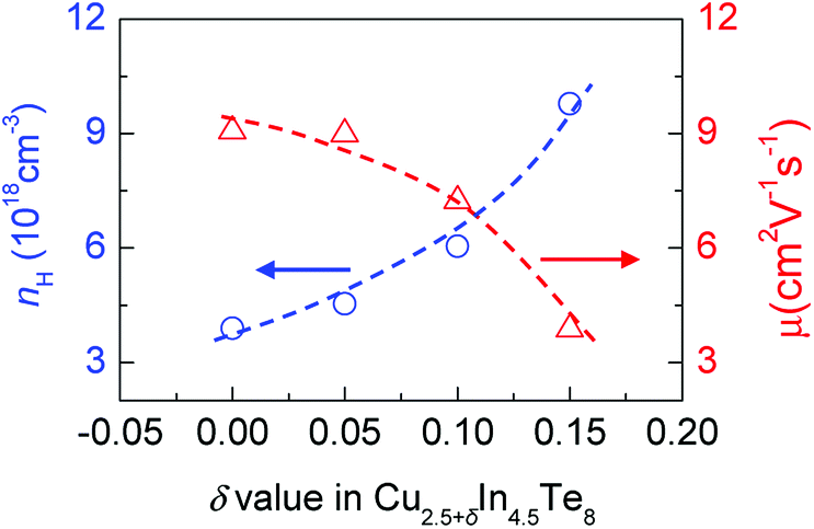 | ||
| Fig. 2 Measured Hall carrier concentration (nH) and mobility (μ) of Cu2.5+δIn4.5Te8 at RT against extra Cu content (δ value). | ||
3.4 Thermoelectric performance
The Seebeck coefficients (α) of different materials against temperature are plotted in Fig. 3a. The α values, which are positive, increase as temperature climbs up to ∼670 K, at which they reach the highest (307–315 μV K−1). Above 670 K the α values decrease rapidly until the temperature reaches 730–755 K, above which they increase or fluctuate with the increase of the temperature. This abnormal behavior might be attributed to the order–disorder transition, which will be discussed below. The Seebeck coefficient below ∼600 K tends to increase when δ value increases, which might be a result of the dominant increase in effective mass (m*). To substantiate this assumption, we plot the dependence of the Seebeck coefficients on the Hall carrier concentration in Fig. 3b, assuming that the Pisarenko relation32 with SPB model is valid in Cu–In–Te systems.18,33 This dependence indicates that the α values of samples with extra Cu (circled by dotted line) are higher than those predicted by Pisarenko relation at the corresponding carrier concentrations. The solid line depicted in Fig. 3b corresponds to the relationship between α and nH for Cu2.5In4.5Te8 (δ = 0) at RT with an effective mass of m* = 0.29 me. Besides, the calculation also reveals the systematic increase of the effective mass from m* = 0.29 me (δ = 0) to 0.58 me (δ = 0.15) (the results are not shown here). It is therefore determined that the effective mass of carrier increases upon an addition of extra Cu. The reason for the increasing of effective mass of carrier is unknown. The possible explanation is that the valence band dispersion gets weaker as the Fermi level moves into the conduction band with increasing of extra Cu. | ||
Fig. 3 (a) Seebeck coefficients of compounds Cu2.5+δIn4.5Te8 (δ = 0, 0.05, 0.1, 0.15) as a function of temperature; (b) experimentally determined Seebeck coefficients (α) at the corresponding Hall carrier concentrations, labeled by     . The solid line represents the Pisarenko relation at RT; (c) electrical conductivities (σ) as a function of temperature for different materials (δ values); (d) power factor PF, PF = α2σ, of different materials (δ values). . The solid line represents the Pisarenko relation at RT; (c) electrical conductivities (σ) as a function of temperature for different materials (δ values); (d) power factor PF, PF = α2σ, of different materials (δ values). | ||
The electrical conductivities (σ) are presented in Fig. 3c as a function of temperature, where it was observed that above ∼730 K the σ values at δ ≥ 0.1 are higher than those at δ ≤ 0.05. This is a result of an enhancement in carrier concentration as δ value increases and the degenerate impurity band at G point (Fig. 2). The highest σ at δ = 0.1 is 6.1 × 10³ Ω−1 m−1 at ∼800 K. Combined with the Seebeck coefficient and electrical conductivity data, we obtained the power factor PF, PF = α2σ, shown in Fig. 3d. Similarly, the materials at δ ≥ 0.1 have higher PF values at high temperatures and the sample at δ = 0.1 gives the highest PF value 3.82 μW cm−1 K−2 at ∼774 K. Likewise, the PF values above ∼730 K increases possibly due to the order–disorder transition of the materials.
Lattice thermal conductivities (κL) of different materials (δ values) are presented in Fig. 3e as a function of temperature. Generally, the curves of lattice part (κL) can be divided into three sections (I, II, III), where the lattice parts in section II, corresponding to the temperature range between 730–770 K, reduce more rapidly than those in section I and III. This temperature range is in accordance with that specified in Fig. 3a, where above ∼730 K the Seebeck coefficients start to increase once more. When the measuring temperature increases to the highest ∼820 K, the lattice part at δ = 0.1 gets the minimum (0.23 W K−1 m−1), which is lower than those (∼0.32 W K−1 m−1) at δ = 0.05 and 0.15. Further, the resemblance between the lattice parts and those of total κ, as shown in the inset Fig. 3e, suggests that the phonon transport plays a major role in heat transfer.
Combined with the three physical parameters (α, σ, κ), we attained the TE figure of merits (ZT) as a function of temperature, as shown in Fig. 3f. The highest ZT value reaches 0.84 at ∼820 K for the sample at δ = 0.1. This value is about 0.38 higher than that of the pristine Cu2.5In4.5Te8.
As mentioned above, the abnormal variations of some physical properties with temperature around 700 K (Fig. 3a and e) are likely related to the order–disorder transition,34–36 that is, a transition from chalcopyrite (s. g. I-42d) to sphalerite structure (s. g. F-43m). The driving force of this transition is a Cu–In antisite occupancy in the critical temperature region35 when the anion position displacement u is less than 0.265 for chalcopyrite compounds34 (the u value of present materials is ∼0.25). The critical temperature might be ∼703 K in the present material system, which was observed in the DSC curve of Cu2.5In4.5Te8, as shown in Fig. S6.† This temperature is in rough accordance with the onset temperature, above which the Seebeck coefficients (Fig. 3a) and lattice thermal conductivity (Fig. 3e) decrease rapidly. Besides, there is less or no indication of element Te evaporation below ∼740 from the DSC curve. Only when the temperature rises to above ∼740 K does the weight loss of the sample occur. Therefore, the scattered data of the TE properties above 740 K is mainly ascribed to the deprivation of gravity. However, we can not rule out the possibility of the reaction between the tiny Cu-precipitates and the matrix at high temperatures, which yields the unexpected change of the TE properties, although the precipitates were not identified using XRD analysis.
In the present material system Cu2.5+δIn4.5Te8, we observed the formation of IB. This IB at G point is highly degenerate in the VBM as δ value increases, which promotes the transport of electrons from the valence band to conduction band (CB), similar to those observed in Mn-doped Cr1.9Mn0.1Ge2Te6,37 Sn-doped Ga2O3 (ref. 38) and Co2+-doped ZnSe39 systems. Therefore, the carrier concentration rises, although many investigations have revealed that the dopant induced IB within the band gap could act as an electron–hole (e–h) recombination centers.40–42
Moreover, an ultralow lattice thermal conductivity (0.23 W K−1 m−1 at δ = 0.1), observed at high temperatures (∼820 K), should result from the dominant lattice disorder along with the phonon–electron interaction. The dominant phonon scattering is caused by the point defect scatterings on the copper vacancy and the antisite defect InCu, and the scattering generated by the structural transition from ordered chalcopyrite to disordered sphalerite structure at high temperatures, whereas the scattering from phonon–electron interaction is a result of the enhanced carrier concentration. However, as more Cu is added in the Cu2.5In4.5Te8 compound, the extra phonon scattering caused by the occupation of extra Cu at copper vacancy should weaken, because the concentration of copper vacancy acting as scattering centers decreases. That is why we have observed relatively higher κL value at δ = 0.15 than that at δ = 0.1 at high temperatures.
In order to confirm the unexpected low κL at δ = 0.1, we performed a theoretical calculation of lattice thermal conductivity based on the Callaway model,43 assuming that the Umklapp and point defect scatterings are the main scattering mechanisms. Below is the ratio of the modeled lattice thermal conductivity of the crystal with the additions of extra Cu, κL, to the measured lattice thermal conductivity of the pristine compound, κL.exp:
 | (1) |
 | (2) |
 | (3) |
Here


In the present work, ε, γ and νp are estimated according to eqn (4–6).43,47,48
 | (4) |
 | (5) |
 | (6) |
According to the above-noted calculations, we thus obtained the scaling parameter (c), mass fluctuations Γm, strain field fluctuations Γs and disorder scattering parameter (Γ = Γm + Γs) of Cu2.5+δIn4.5Te8 compounds and listed them in Table 3. The estimated lattice thermal conductivities (κL) at 330 K, 670 K and 820 K are presented in Fig. 4, where the lattice part κL at δ = 0.2 were measured specifically for a better visual presentation. We observed in Fig. 4 that the estimated values are in good agreement with those from experimental data except for the sample (δ = 0.05) at 330 K and 670 K, whose calculated values are a little higher than those from the measurement. The reason might be that we did not take the grain boundary scattering of phonons on the precipitated secondary phases into account, although these tiny phases have not been identified using XRD analysis yet. These calculations showcase the possibility of ultralow lattice thermal conductivity upon a proper addition of extra Cu in the samples.
| δ | c | Γm | Γs | Γ |
|---|---|---|---|---|
| 0.05 | 58.95 | 0.0034 | 1.8005 | 1.8039 |
| 0.10 | 81.99 | 0.0043 | 3.4852 | 3.4895 |
| 0.15 | 99.36 | 0.0052 | 5.1198 | 5.1250 |
| 0.2 | 113.70 | 0.0060 | 6.7045 | 6.7105 |
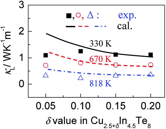 | ||
| Fig. 4 Estimated lattice thermal conductivities (κL) as a function of extra Cu content (δ value) at 330 K, 670 K and 820 K using Callaway model. The measured κL,exp. values are also shown for comparison. | ||
4. Conclusions
We prepared the ternary copper-deficient compounds Cu2.5+δIn4.5Te8 (δ = 0–0.15) and examined their band structure and TE performance. The first-principles calculations reveal that there is an impurity band (IB) within the gap. The IB at G point is highly degenerate at the valence band maximum, which is responsible for an enhancement in Hall carrier concentration (nH) and electrical conductivity (σ) as δ value increases. Also, we observed an ultralow lattice thermal conductivity (only 0.23 W K−1 m−1) in the sample at δ = 0.1 and 820 K resulting from an increased lattice disorder. We further confirmed our findings through calculation using the Callaway model. We thus obtained the highest thermoelectric figure of merit ZT of 0.84. This value is about 0.38 higher than that of the pristine Cu2.5In4.5Te8.Conflicts of interest
There are no conflicts of interest to declare.Acknowledgements
This work is supported by the National Natural Science Foundation of China (51671109, 51171084)Notes and references
- K. F. Hsu, S. Loo, F. Guo, W. Chen, J. S. Dyck, C. Uher, T. Hogan, E. K. Polychroniadis and M. G. Kanatzidis, Science, 2004, 303, 818 CrossRef PubMed
.
- B. Poudel, Q. Hao, Y. Ma, Y. Lan, A. Minnich, B. Yu, X. Yan, D. Wang, A. Muto, D. Vashaee, X. Chen, J. Liu, M. S. Dresselhaus, G. Chen and Z. Ren, Science, 2008, 320, 634 CrossRef PubMed
- Y. Pei, X. Shi, A. LaLonde, H. Wang, L. Chen and G. J. Snyder, Nature, 2011, 473, 66 CrossRef PubMed
- J. P. Heremans, V. Jovovic, E. S. Toberer, A. Saramat, K. Kurosaki, A. Charoenphakdee, S. Yamanaka and G. J. Snyder, Science, 2008, 321, 554 CrossRef PubMed
- H. Liu, X. Shi, F. Xu, L. Zhang, W. Zhang, L. Chen, Q. Li, C. Uher, T. Day and G. J. Snyder, Nat. Mater., 2012, 11, 422 CrossRef PubMed
- H. Liu, X. Yuan, P. Lu, X. Shi, F. Xu, Y. He, Y. Tang, S. Bai, W. Zhang, L. Chen, Y. Lin, L. Shi, H. Lin, X. Gao, X. Zhang, H. Chi and C. Uher, Adv. Mater., 2013, 25, 6607 CrossRef PubMed
- W. Zhao, Z. Liu, P. Wei, Q. Zhang, W. Zhu, X. Su, X. Tang, J. Yang, Y. Liu, J. Shi, Y. Chao, S. Lin and Y. Pei, Nat. Nanotechnol., 2017, 12, 55 CrossRef PubMed
- W. Zhao, Z. Liu, Z. Sun, Q. Zhang, P. Wei, X. Mu, H. Zhou, C. Li, S. Ma, D. He, P. Ji, W. Zhu, X. Nie, X. Su, X. Tang, B. Shen, X. Dong, J. Yang, Y. Liu and J. Shi, Nature, 2017, 549, 247 CrossRef PubMed
- Y. Pei, Z. M. Gibbs, A. Gloskovskii, B. Balke, W. G. Zeier and G. J. Snyder, Adv. Energy Mater., 2014, 4, 1400486 CrossRef
- R. Liu, L. Xi, H. Liu, X. Shi, W. Zhang and L. Chen, Chem. Commun., 2012, 48, 3818 RSC
- O. Yarema, M. Yarema, W. M. M. Lin and V. Wood, Chem. Commun., 2016, 52, 10878 RSC
- J. Wei, H. J. Liu, L. Cheng, J. Zhang, J. H. Liang, P. H. Jiang, D. D. Fan and J. Shi, AIP Adv., 2015, 5, 107230 CrossRef
- A. Kosuga, K. Umekage, M. Matsuzawa, Y. Sakamoto and I. Yamada, Inorg. Chem., 2014, 53, 6844 CrossRef PubMed
- T. Plirdpring, K. Kurosaki, A. Kosuga, M. Ishimaru, Y. Ohishi, H. Muta and S. Yamanaka, Phys. Status Solidi RRL, 2012, 6, 154 CrossRef
- M. Parlak, Ç. Ercelebi, İ. Günal, H. Özkan, N. M. Gasanly and A. Çulfaz, Cryst. Res. Technol., 1997, 32, 395 CrossRef
- E. Guedeza, L. Mogollónb, G. Marcanoa, S. M. Wasima, G. Sánchez Péreza and C. Rincón, Mater. Lett., 2017, 186, 155 CrossRef
- E. Guedez, C. Rincón, S. M. Wasim, G. E. Delgado, G. Marcano and G. Sánchez-Pérez, Phys. Status Solidi B, 2017, 254, 1700087 CrossRef
- R. Liu, Y. Qin, N. Cheng, J. Zhang, X. Shi, Y. Grin and L. Chen, Inorg. Chem. Front., 2016, 3, 1167 RSC
- J. Zhang, R. Liu, N. Cheng, Y. Zhang, J. Yang, C. Uher, X. Shi, L. Chen and W. Zhang, Adv. Mater., 2014, 26, 3848 CrossRef PubMed
- X. Shi, L. Chen and C. Uher, Int. Mater. Rev., 2016, 61, 379 CrossRef
- J. Shen, Z. Chen, S. Lin, L. Zheng, W. Li and Y. Pei, J. Mater. Chem. A, 2016, 4, 15464 RSC
- A. Yusufu, K. Kurosaki, A. Kosuga, T. Sugahara, Y. Ohishi, H. Muta and S. Yamanaka, Appl. Phys. Lett., 2011, 99, 061902 CrossRef
- A. Kosuga, T. Plirdpring, R. Higashine, M. Matsuzawa, K. Kurosaki and S. Yamanaka, Appl. Phys. Lett., 2012, 100, 042108 CrossRef
- Z. Xia, G. Wang, X. Zhou and W. Wen, Ceram. Int., 2017, 43, 16276 CrossRef
- H. Kim, Z. M. Gibbs, Y. Tang, H. Wang and G. J. Snyder, APL Mater., 2015, 3, 041506 CrossRef
- G. Kresse and J. Furthmuller, Phys. Rev. B, 1996, 54, 11169 CrossRef
- G. Kresse and J. Furthmuller, Comput. Mater. Sci., 1996, 6, 15 CrossRef
- M. Nolan, S. C. Parker and G. W. Watson, Surf. Sci., 2005, 595, 223 CrossRef
- P. E. Blöchl, Phys. Rev. B: Condens. Matter, 1994, 50, 17953 CrossRef
- J. P. Heremans, B. Wiendlochaac and A. M. Chamoire, Energy Environ. Sci., 2012, 5, 5510 RSC
- B. Wiendlocha, J.-B. Vaney, C. Candolfi, A. Dauscher, B. Lenoirb and J. Tobola, Phys. Chem. Chem. Phys., 2018, 20, 12948 RSC
- G. J. Snyder and E. S. Toberer, Nat. Mater., 2008, 7, 105 CrossRef PubMed
- N. Cheng, R. Liu, S. Bai, X. Shi and L. Chen, J. Appl. Phys., 2014, 115, 163705 CrossRef
- A. Zunger, Appl. Phys. Lett., 1987, 50, 164 CrossRef
- S. Schorr, G. Geandier and B. V. Korzun, Phys. Status Solidi, 2006, 3, 2610 CrossRef
- C. Rincón, Solid State Commun., 1987, 64, 663 CrossRef
- X. Tang, D. Fan, K. Peng, D. Yang, L. Guo, X. Lu, J. Dai, G. Wang, H. Liu and X. Zhou, Chem. Mater., 2017, 29, 7401 CrossRef
- X. Zhao, Z. Wu, W. Cui, Y. Zhi, D. Guo, L. Li and W. Tang, ACS Appl. Mater. Interfaces, 2017, 9, 983 CrossRef PubMed
- N. S. Norberg, G. M. Dalpian, J. R. Chelikowsky and D. R. Gamelin, Nano Lett., 2006, 6, 2887 CrossRef PubMed
- M. Cheng, S. Chen, Z. Du, X. Liu and J. Cui, Phys. Status Solidi A, 2016, 213, 2176 CrossRef
- X. Hou, S. Chen, Z. Du, X. Liu and J. Cui, RSC Adv., 2015, 5, 102856 RSC
- L. Zhang, Q. Zheng, Y. Xie, Z. Lan, O. V. Prezhdo, W. A. Saidi and J. Zhao, Nano Lett., 2018, 18, 1592 CrossRef PubMed
- J. Callaway and H. C. Von Baeyer, Phys. Rev., 1960, 120, 1149 CrossRef
- B. Fernández and S. M. Wasim, Phys. Status Solidi, 1990, 122, 235 CrossRef
- K. Kurosaki, A. Kosuga, H. Muta, M. Uno and S. Yamanaka, Appl. Phys. Lett., 2005, 87, 061919 CrossRef
- B. Abeles, Phys. Rev., 1963, 131, 1906 CrossRef
- C. L. Wan, W. Pan, Q. Xu, Y. X. Qin, J. D. Wang, Z. X. Qu and M. H. Fang, Phys. Rev. B: Condens. Matter Mater. Phys., 2006, 74, 144109 CrossRef
- D. S. Sanditov and V. N. Belomestnykh, Tech. Phys., 2011, 56, 1619 CrossRef
Footnote |
| † Electronic supplementary information (ESI) available. See DOI: 10.1039/c8ra05188g |
| This journal is © The Royal Society of Chemistry 2018 |