
 Open Access Article
 This Open Access Article is licensed under a Creative Commons Attribution-Non Commercial 3.0 Unported Licence
A simple method to improve the performance of perovskite light-emitting diodes via layer-by-layer spin-coating CsPbBr3 quantum dots†
Bobo Li‡
 a,
Xiaomeng Li‡a,
Xia Lib,
Haolin Liua,
Zhaonan Lia,
Guohong Xianga,
Yuhan Liua,
Taojie Zhoua,
Xuan Fanga and
Zhaoyu Zhang*a
a,
Xiaomeng Li‡a,
Xia Lib,
Haolin Liua,
Zhaonan Lia,
Guohong Xianga,
Yuhan Liua,
Taojie Zhoua,
Xuan Fanga and
Zhaoyu Zhang*a
aSchool of Science and Engineering, The Chinese University of Hong Kong, Shenzhen, Guangdong 518172, P. R. China. E-mail: zhangzy@cuhk.edu.cn
bState Key Laboratory of Inorganic Synthesis and Preparation Chemistry, College of Chemistry, Jilin University, Changchun, 130012, P. R. China
First published on 31st July 2018
Abstract
Recently, all-inorganic halide perovskite quantum dots have become a very promising material for light-emitting diodes. Herein, we demonstrate a facile method, namely, layer-by-layer spin-coating of CsPbBr3 QDs to improve device performance. After optimization of the number of emissive layers, the maximum EQE can be increased from an initial value of 0.69% to 2.31%. Additionally, we inserted a CBP layer between PEDOT:PSS and CsPbBr3 multilayers to balance charge transportation and recombination. As a result, a 37% improvement in EQE (up to 3.16%) and highest luminance of 2629 cd m−2 are obtained.
Introduction
In the past ten years, halide perovskite materials AMX3 (where A = CH3NH3+, HC(NH2)2+, Cs+; M = Pb2+, Sn2+; X = Cl−, Br−, I−) have attracted increasing attention due to their unique optoelectronic properties, such as a broad light-absorption spectrum, tunable optical band-gap, high color purity and tunability, good hole and electron-transport capability, low cost and easy preparation technology.1–6 Perovskite materials have been widely applied in solar cells, light-emitting diodes, lasers and photodetectors, etc.In 2014, Friend et al. first reported the hybrid organic–inorganic CH3NH3PbBr3 based perovskite light-emitting diode (PeLED) with maximum external quantum efficiency (EQE) of 0.76%.7 Since then, the performance of PeLED has been rapidly improved. Within only one year, the maximum EQE of the CH3NH3PbBr3 based PeLED was drastically increased to 8.53%.8 Additionally, Wang et al. reported a red PeLED based on mixed organic cation multiple quantum well perovskites, which can maintain a high EQE of up to 12.7%.9 These results indicate that PeLEDs can be competitive with organic LEDs. However, organic–inorganic perovskites suffer chemical instabilities under conditions of moisture or oxygen, which limits further development of PeLEDs for commercial applications.
Comparing with organic cation-based lead-halide perovskites, all-inorganic perovskites, such as CsPbX3 (X is usually Br, Cl, I or mixed halide), exhibit improved chemical and thermal stability in ambient atmosphere. Moreover, all-inorganic perovskites usually have the merits of high photoluminescence quantum yield and narrow emissions.10 In 2015, Yantara et al. first applied CsPbBr3 films in PeLED.11 Concurrently, Zeng et al. reported CsPbX3 quantum dots (QDs)-based PeLED with a maximum EQE of only 0.12%.12 In the following three years, tremendous efforts have been focused on perovskite films or QDs optimization and device engineering in order to enhance the performance of all-inorganic PeLED. For example, Rogach et al. achieved an EQE of 0.35% by using an insulating material as a solution additive or with an additional hole-blocking layer in CsPbBr3-based PeLED.13 Pan et al. employed a short ligand exchange strategy to grow CsPbBr3 nanocrystals with the maximum EQE of the green PeLED reaching 3%. They also used similar method to fabricate a mixed-anion CsPbBrxCl3−x-based device and achieved a high EQE value of 1.9% for the blue-emitting PeLED.14 Subsequently, Zeng et al. improved the EQE value to 6.27% for solution-processed CsPbBr3-based device, through balancing surface passivation and carrier injection via ligand density control.15 Recently, they further demonstrated a peak EQE of CsPbBr3 based PeLED at 11.6% via room-temperature triple-ligand surface engineering.16 Additionally, Li et al. demonstrated a simple trimethylaluminum (TMA) crosslinking technique in red-emitting LED based on CsPbI3 nanocrystals and obtained a remarkable EQE as high as 5.7%.17 Other methods to improve the performance of all-inorganic PeLEDs, such as polymer-assisted method,18,19 small molecule-assisted method,20 device interfacial engineering and emitter-doped method,21–23 have also been reported, which boosted strategies for research.
Nevertheless, all these studies focused on separating QDs to avoid aggregation quenching, for which precise control of ligand, doping or surface passivation were needed, thus increasing the complexity of the fabrication process. Therefore, it is necessary to explore strategies, alternative to the aforementioned attempts, to improve the efficiency of PeLEDs. It is known that the QDs can be uniformly dispersed and the phenomenon of aggregation can be greatly reduced if the concentration of dispersion is lowered. However, lower concentration would cause the decrease in the number of QDs in a single emissive layer, thus influencing the light-emitting efficiency. In view of this concern, we proposed a novel and facile approach for highly-efficient green-emitting PeLED via deposition of multilayers of low concentration of CsPbBr3 QDs dispersion without specific chemical treatment, which can effectively simplify the process of device fabrication. Additionally, the device performance can be further improved by incorporating a 4,4′-bis(N-carbazolyl)-1,1′-biphenyl (CBP) layer between poly(3,4-ethylenedioxythiophene)–poly(styrenesulfonate) (PEDOT:PSS) and emitting layer. CBP can balance charge transportation and recombination. As a result, the optimized device with CsPbBr3 multilayers exhibits luminance of 1923 cd m−2 and maximum EQE of 2.31% (at 5.6 V), which are higher than the device with single layer of QDs. In addition, EQE can achieve about 37% improvement on the basis of the multilayers-based device on introducing a CBP layer between PEDOT:PSS and CsPbBr3 layers.
Experimental section
Materials
Indium tin oxide (ITO) substrates (thickness of 185 nm, sheet resistance ≤ 6 Ω, transmittance ≥ 84%) were purchased from South China Science & Technology Company, Shenzhen. PEDOT:PSS (4083), CBP (purity > 99%), 1,3,5-tris(1-phenyl-1H-benzimidazol-2-yl)benzene (TPBI, purity > 99%) and lithium fluoride (LiF) were obtained from Xi'an Polymer Light Technology Company. All solvents were purchased from J&K Scientific, Ltd (China) unless otherwise indicated. All chemicals were used without further purification.Device fabrication
ITO substrates were cleaned sequentially in ultrasonic solvent baths of deionized water, acetone and isopropyl alcohol for 15 min, in sequence. Then, the substrates were blow-dried with nitrogen and then treated with oxygen-plasma for 8 min. PEDOT:PSS was spin-coated onto the ITO substrates at 3000 rpm for 60 s and then baked at 130 °C for 20 min. Subsequently, ITO/PEDOT:PSS samples were transferred into a vacuum thermal evaporation chamber to deposit a CBP layer. The evaporation rate and thickness of the coating were 0.3 Å s−1 and 15 nm, respectively. CsPbBr3 QDs were synthesized as reported previously and provided by our collaborators.24 For the perovskite layer, the as-prepared CsPbBr3 QDs were first dispersed in tetrahydrofuran (THF) at a concentration of 2 mg mL−1 under continuous stirring for 1 hour. Then, the solution was treated with static settlement over 48 hours in a glove box and consequently, distinct delamination was observed. We dipped the supernatant onto the treated substrates and spin-coated at 2000 rpm for 40 s. We repeated the above step several times in order to obtain samples with multilayers of CsPbBr3. Finally, the samples were loaded into a glovebox-integrated deposition chamber once again and pumped down to a pressure of <10−4 Pa. TPBI (30 nm), LiF (1 nm) and Al (100 nm) layers were sequentially deposited by thermal evaporation through a shadow mask at rates of 0.3 Å s−1, 0.2 Å s−1 and 2 Å s−1, respectively.Device characterization
Transmission electron microscopy (TEM) image was recorded by using JSM-3100F FETEM. UV-vis spectra were obtained from Shimadzu UV-1750 UV-visible spectrophotometer. Photoluminescence (PL) measurements were performed using Ocean Optics Spectrometer (Maya 2000 PRO). Images of film surface morphology and device cross-section were acquired from scanning electron microscopy (MAlA3 model 2016, TESCAN). Thickness of the perovskite films was measured using an atomic force microscope (AFM, Bruker). Current–voltage and electroluminescence (EL) properties of PeLEDs were measured using a semiconductor characterization analyzer (Keithley 2634B) and Maya Spectrometer. Luminance–current density values were recorded by using a ST 86LA luminance meter. Results of EQE were obtained from the system of integrating sphere combined with Ocean Optics Spectrophotometer.Results and discussion
Fig. 1(a) shows the TEM image of the nanocrystals. We can clearly see that these particles exhibit a cubic shape with an average size of about 20 nm. Fig. 1(b) shows a photograph of the QDs dispersion taken under UV light irradiation. Multilayers (1 to 5 layers) of CsPbBr3 QDs films were fabricated by pipetting and spin-coating the supernatant. Then, we compared the optical characteristics of the films of single CsPbBr3 layer, multiple CsPbBr3 layers (4 layers) and CBP/CsPbBr3 multilayers (4 layers). Normalized absorption and PL spectra of these three types of films are shown in Fig. 1(c), displaying similar absorption transitions. We also can see that their normalized PL spectra are overlapped. The PL emission peaks for all the films are located at around 520 nm and the full width at half maximum (FWHM) is only 18 nm. These results indicate that the optical performance stays unchanged with the increase in layers of CsPbBr3 QDs. In addition, insertion of the CBP layer has no influence on the PL spectra.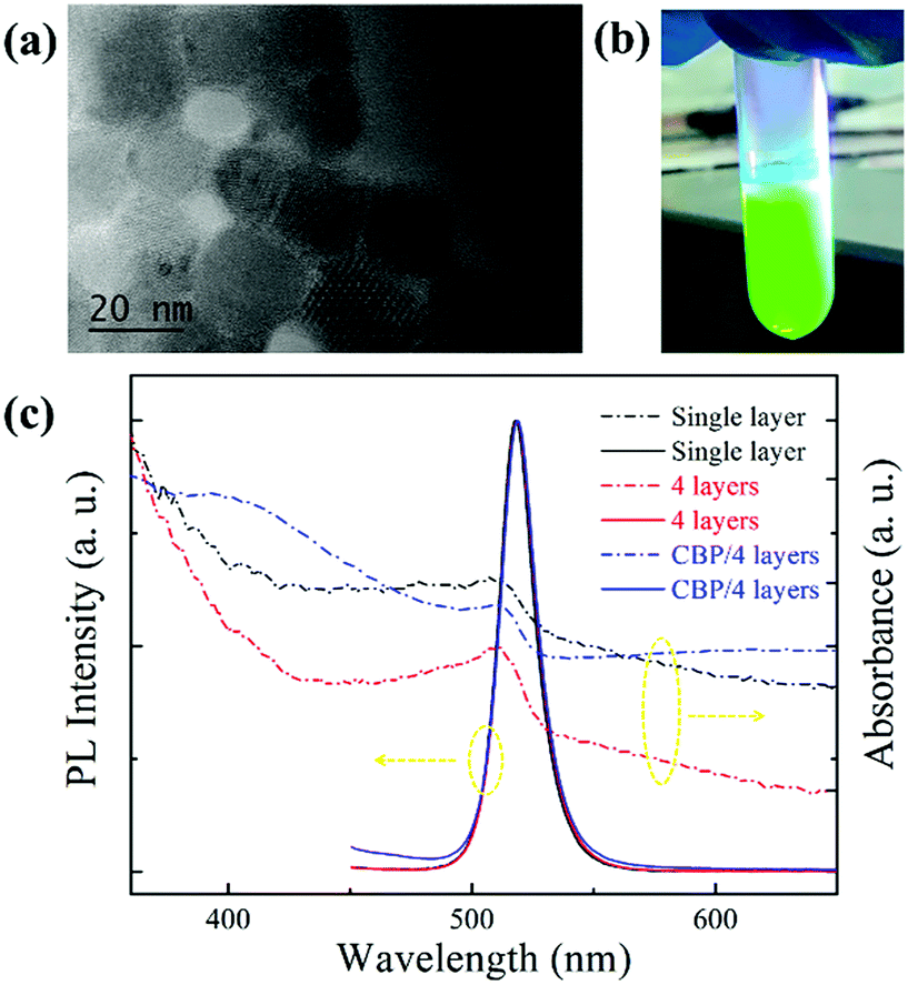 | ||
| Fig. 1 (a) TEM image of CsPbBr3 QDs. (b) Photograph of CsPbBr3 solution with UV light irradiation. (c) UV-vis absorption and PL spectra of three types of films on glass substrates (single layer of CsPbBr3, 4 layers of CsPbBr3 and CBP/4 layers of CsPbBr3). | ||
In order to investigate the influence of concentration and number of spin-coated layers on the film surface morphology, we performed SEM measurements, and the images are exhibited in Fig. 2.
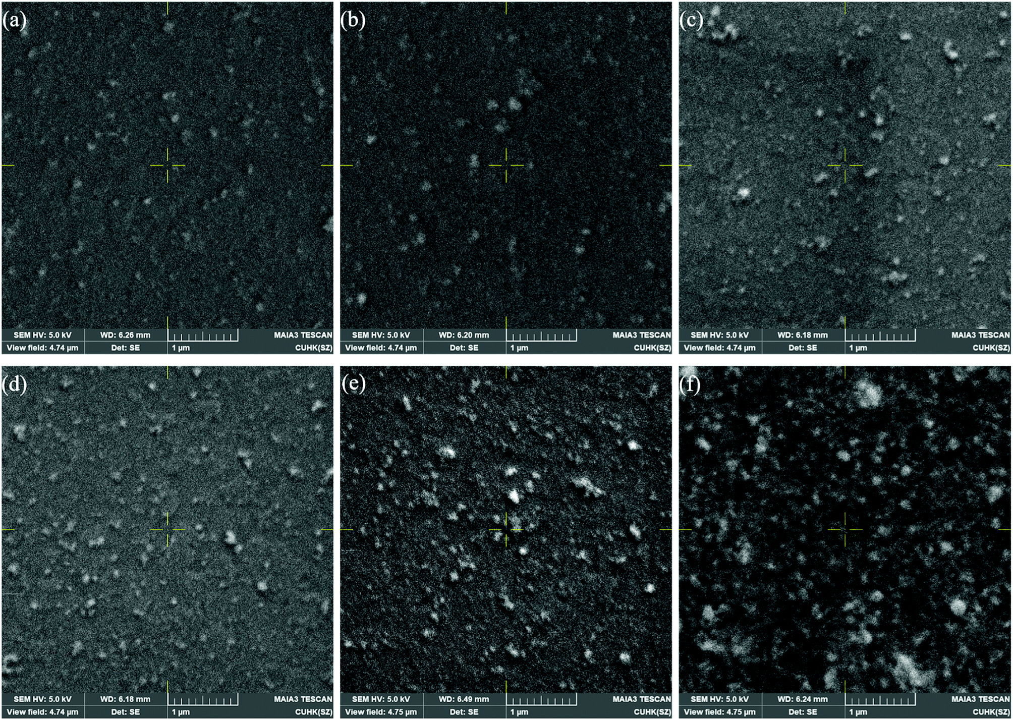 | ||
| Fig. 2 SEM images of CsPbBr3 perovskite films (low concentration of QDs, 2 mg mL−1) for different layers: (a) single layer, (b) two layers, (c) three layers, (d) four layers and (e) five layers. (f) Surface morphology of single layer of perovskite film deposited from high concentration of CsPbBr3 QDs (10 mg mL−1). All perovskite films were prepared on ITO substrates. | ||
From Fig. 2(a–e), we can see that the surfaces of films with low concentration of QDs are relatively smooth and uniform when compared with the surface of the film spin-coated from high concentration of CsPbBr3 QDs solution (Fig. 2(f)). In addition, QDs aggregation is very low in the single layer of perovskite film. However, it becomes severely agminated when the layers of QDs are continuously increased.
We also measured the thickness of the perovskite films with different layers using AFM, as shown in Fig. S1 (ESI†). All the films exhibit similar thickness in the range of 30–40 nm. Thus, we can conclude that the thickness is not dependent on the number of spin-coated layers.
Fig. 3(a) exhibits the device configuration of the three PeLED devices fabricated in this study. Device A represents PeLED with a single-layer of CsPbBr3 QDs. Device B comprises multiple layers (4 layers) of CsPbBr3 QDs. Device C is the CBP-modified structure with CsPbBr3 multilayers (4 layers), and is composed of indium thin oxide (ITO), poly(3,4-ethylenedioxythiophene) polystyrene sulfonate (PEDOT:PSS), CBP, CsPbBr3 QDs (4 layers), 2,2′,2′′-(1,3,5-benzinetriyl)-tris(1-phenyl-1H-benzimidazole) (TPBi), LiF and Al. Perovskite multilayers were formed by layer-by-layer deposition. Active area of these devices is 0.12 cm2. Fig. S2 (ESI†) exhibits the cross-sectional SEM image of PeLED based on 4 layers of QDs. In addition, the energy level diagram of each layer of Device C, as a representative, is shown in Fig. 3(b). We inserted a 15 nm CBP layer, which can block electrons in the active layer, between PEDOT:PSS and CsPbBr3. This balanced the charge transportation and improved efficiency of charge recombination in the device. Simultaneously, the hole injection barrier does not increase further, as shown in energy-level diagram, due to the well-matched HOMO level between CBP and CsPbBr3 QDs.
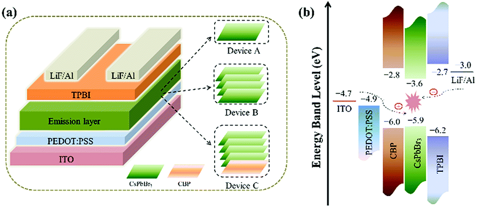 | ||
| Fig. 3 (a) Schematics of the three types of PeLED devices. (b) Energy levels of various device components in the PeLED. | ||
To evaluate the influence of the number of layers of emissive material on the device performance, we investigated the devices based on 1 to 5 layers of CsPbBr3 QDs; the results are recorded in Fig. 4 and Table 1. Fig. 4(a) exhibits the electroluminescence (EL) spectra of the different devices, which were electrically driven in constant current mode of 20 mA. We observe that all the emission peaks are located at around 520 nm and FWHM is as low as 18 nm, which indicates high color purity. EL intensity increased gradually when the number of layers was no more than four. Similar variation can be found in the maximum values of EQE, as shown in Fig. 4(b). The device based on 4 layers of CsPbBr3 QDs exhibits the highest EQE of 2.31% (at 5.6 V), which is almost 3.4-fold higher than that of the single-layer based device (0.69% at 6.3 V). The maximum luminance improved to 1923 cd m−2 from an initial value of 618 cd m−2. However, the device performance decreased upon further increasing the number of QD layer (>4 layers). We speculate that the average increment of EQE with the increase in number of coating layers is mainly promoted by more excitons formation in the emissive layer. Maximum EQE and luminance appeared in the 4 layers-based device. Therefore, although the concentration of perovskite QDs is effectively increased, slight aggregation of QDs does not hamper the device performance. The decrease in device performance is mainly attributed to concentration-quenching or self-quenching.25,26 These results are consistent with the results of SEM surface morphology analysis. Moreover, the thicknesses of different numbers of QD layers, measured by AFM and profilometer, are closely matched even if we add more number of coating layers because the QDs from the upper layers may permeate into the former layers on the substrates, which may cause the overlapping of the layers. Then, it is reasonable to assume that concentration increase, rather than the emission zone enlargement, attributed to the decline in device efficiency. In addition, our method reduces the optimized concentration of the colloidal perovskite quantum dots as emissive layer, which is believed to be a key factor in PeLED devices. Additionally, we compared the current–voltage characteristics and the J–V curves, as shown in Fig. S3 (ESI†). The driving voltage increased from 3 V to 4.2 V (current density at 20 mA cm−2) upon increasing the number of CsPbBr3 emissive layers, which is attributed to the increase in resistance in the device.
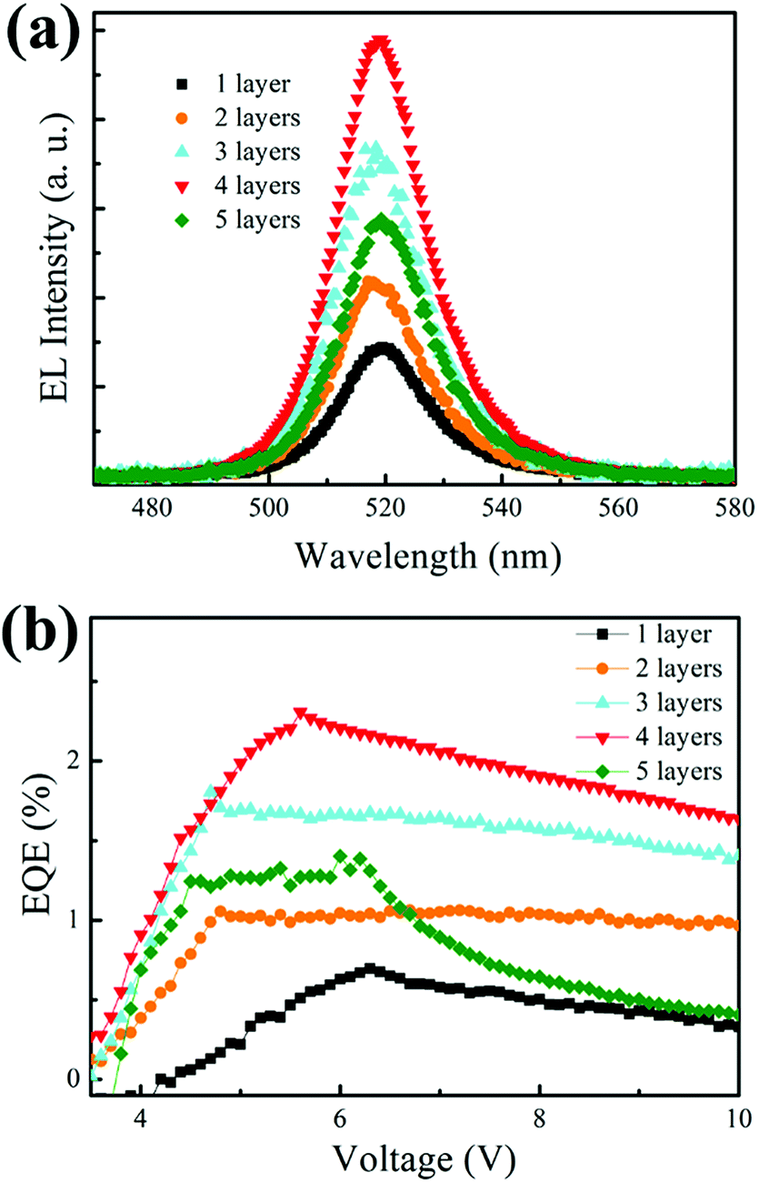 | ||
| Fig. 4 (a) Electroluminescence spectra and (b) EQE–voltage characteristic curves of PeLED based on different layers of CsPbBr3 QDs (1–5 layers). | ||
| Device | Vdriving (V) | Lmax (cd m−2) | EQE (%) |
|---|---|---|---|
| CsPbBr3 (1 layer) | 3.10 | 618 | 0.69 |
| CsPbBr3 (2 layers) | 3.13 | 1063 | 1.05 |
| CsPbBr3 (3 layers) | 3.25 | 1781 | 1.81 |
| CsPbBr3 (4 layers) | 3.87 | 1923 | 2.31 |
| CsPbBr3 (5 layers) | 4.16 | 1470 | 1.40 |
| CBP/CsPbBr3 (4 layers) | 4.23 | 2629 | 3.16 |
Finally, we further improved the device performance by introducing the CBP layer for the as-optimized PeLED with 4 layers of CsPbBr3 QDs. The relevant results of these two types of devices are summarized in Fig. 5 and Table 1. EL spectra can be seen in Fig. 5(a) and the photograph of the uniform bright green emission of CBP-based device (captured by a digital camera) is displayed in the inset. The Commission International de I'Eclairage (CIE) color of the green emission is measured with coordinates of (0.1117, 0.7691), as shown in Fig. S4 (ESI†). The insertion of CBP in the device would also cause the increase in driving and turn-on voltages at 1 cd m−2, which are 3.3 V and 3.5 V, respectively. However, the maximum EQE of the CBP-based PeLED was significantly enhanced from 2.31% to 3.16%. Additionally, fast degradation occurred when current density was over 80 mA cm−2, while maximum luminance of 2629 cd m−2 was obtained from the device with the CBP layer.
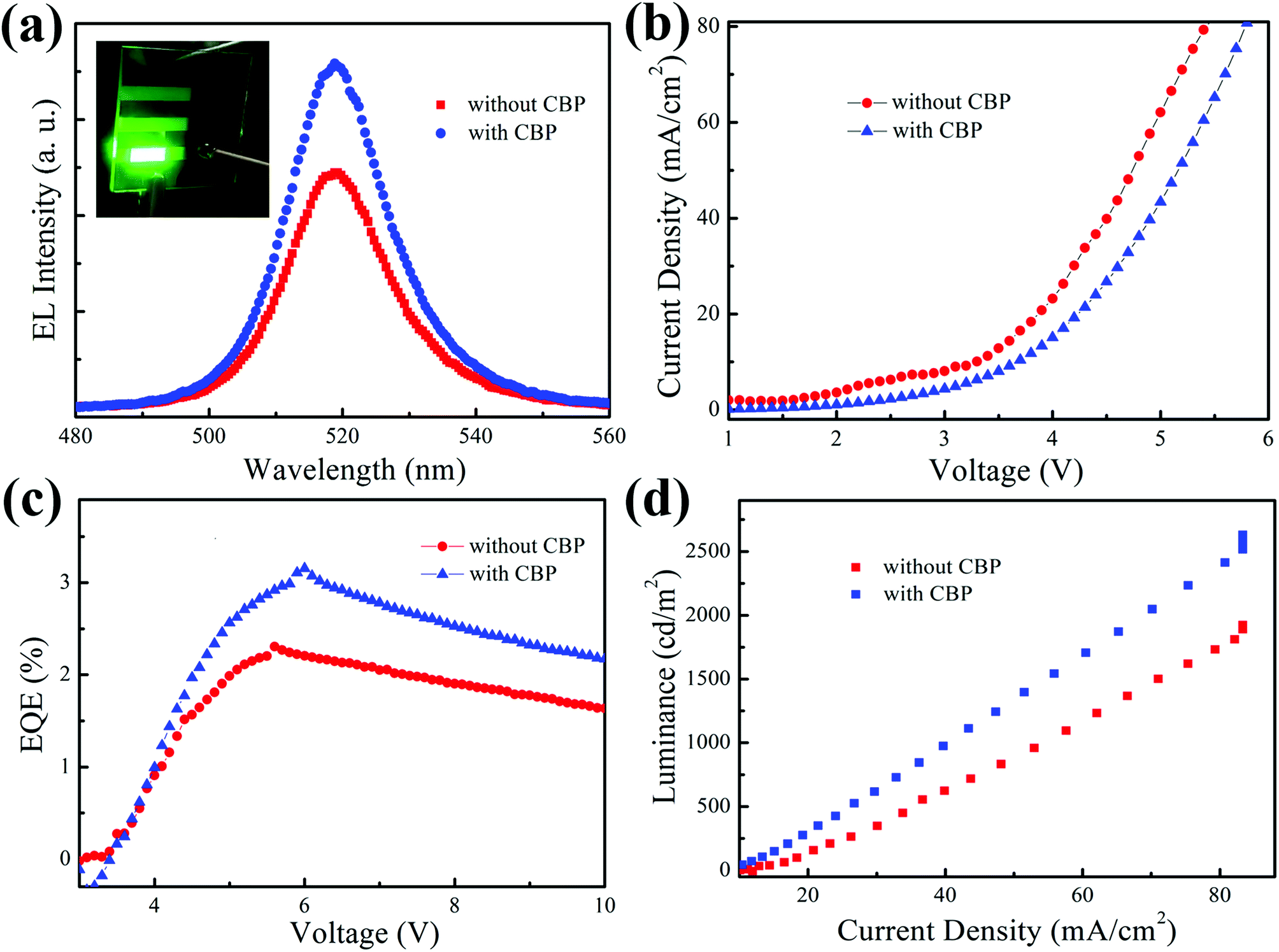 | ||
| Fig. 5 Light-emitting characteristics of PeLED devices with and without CBP: (a) EL spectra, (b) current density–voltage curves, (c) EQE–voltage curves and (d) luminance–current density curves. | ||
All of the above results indicate that the device with CBP layer has a wide band gap, which can effectively confine the electrons in the emitting layer and balance the charge transportation, thus resulting in highly-efficient charge recombination in the perovskite emissive layer.
Conclusions
In conclusion, we report a facile method for the preparation of highly-efficient perovskite LED by successively spin-coating multilayers of CsPbBr3 QDs in this study. Maximum EQE increased up to 2.31% from an initial value of 0.69% upon gradually increasing the number of layers of CsPbBr3 QDs from 1 to 4. However, the device performance declined upon further increasing the number of perovskite QDs layers, which was due to concentration quenching. Additionally, we introduced an energy level-matched CBP layer between PEDOT:PSS and CsPbBr3 layers in the optimized 4 multilayers based-device to balance the charge transportation and recombination. The device with the CBP layer can achieve maximum EQE of 3.16% and maximum luminance of 2629 cd m−2. Therefore, the strategy reported in this paper is promising for improving the light-emitting performance of PeLED.Conflicts of interest
There are no conflicts to declare.Acknowledgements
This research was supported by the National Natural Science Foundation of China (61605036, 61404009, 11474365), Shenzhen Key Laboratory Project under Grant No. ZDSYS201603311644527, Shenzhen Fundamental Research Fund under Grant No. JCYJ20150611092848134 and JCYJ20150929170644623, and the Shenzhen Science and Technology Innovation Fund (KQCX20140522143114399), and the Developing Project of Science and Technology of Jilin Province (20160520117JH).Notes and references
- S. D. Stranks, G. E. Eperon, G. Grancini, C. Menelaou, M. J. Alcocer, T. Leijtens, L. M. Herz, A. Petrozza and H. J. Snaith, Science, 2013, 342, 341–344 CrossRef PubMed.
- S. A. Veldhuis, P. P. Boix, N. Yantara, M. Li, T. C. Sum, N. Mathews and S. G. Mhaisalkar, Adv. Mater., 2016, 28, 6804–6834 CrossRef PubMed.
- Q. Shan, J. Song, Y. Zou, J. Li, L. Xu, J. Xue, Y. Dong, B. Han, J. Chen and H. Zeng, Small, 2017, 13, 1701770 CrossRef PubMed.
- L. Gil-Escrig, A. Miquel-Sempere, M. Sessolo and H. J. Bolink, J. Phys. Chem. Lett., 2015, 6, 3743–3748 CrossRef PubMed.
- N. F. Jamaludin, N. Yantara, Y. F. Ng, A. Bruno, B. K. Chandran, X. Y. Chin, K. Thirumal, N. Mathews, C. Soci and S. Mhaisalkar, J. Mater. Chem. C, 2018, 6, 2295–2302 RSC.
- B. Li, C. Zheng, H. Liu, J. Zhu, H. Zhang, D. Gao and W. Huang, ACS Appl. Mater. Interfaces, 2016, 8, 27438–27443 CrossRef PubMed.
- Z. K. Tan, R. S. Moghaddam, M. L. Lai, P. Docampo, R. Higler, F. Deschler, M. Price, A. Sadhanala, L. M. Pazos, D. Credgington, F. Hanusch, T. Bein, H. J. Snaith and R. H. Friend, Nat. Nanotechnol., 2014, 9, 687–692 CrossRef PubMed.
- H. Cho, S.-H. Jeong, M.-H. Park, Y.-H. Kim, C. Wolf, C.-L. Lee, J. H. Heo, A. Sadhanala, N. Myoung, S. Yoo, S. H. Im, R. H. Friend and T.-W. Lee, Science, 2015, 350, 1222–1225 CrossRef PubMed.
- W. Zou, R. Li, S. Zhang, Y. Liu, N. Wang, Y. Cao, Y. Miao, M. Xu, Q. Guo, D. Di, L. Zhang, C. Yi, F. Gao, R. H. Friend, J. Wang and W. Huang, Nat. Commun., 2018, 9, 608 CrossRef PubMed.
- B. Liu, L. Wang, H. Gu, H. Sun and H. V. Demir, Adv. Opt. Mater., 2018, 6, 1800220 CrossRef.
- N. Yantara, S. Bhaumik, F. Yan, D. Sabba, H. A. Dewi, N. Mathews, P. P. Boix, H. V. Demir and S. Mhaisalkar, J. Phys. Chem. Lett., 2015, 6, 4360–4364 CrossRef PubMed.
- J. Song, J. Li, X. Li, L. Xu, Y. Dong and H. Zeng, Adv. Mater., 2015, 27, 7162–7167 CrossRef PubMed.
- H. Huang, H. Lin, S. V. Kershaw, A. S. Susha, W. C. Choy and A. L. Rogach, J. Phys. Chem. Lett., 2016, 7, 4398–4404 CrossRef PubMed.
- J. Pan, L. N. Quan, Y. Zhao, W. Peng, B. Murali, S. P. Sarmah, M. Yuan, L. Sinatra, N. M. Alyami, J. Liu, E. Yassitepe, Z. Yang, O. Voznyy, R. Comin, M. N. Hedhili, O. F. Mohammed, Z. H. Lu, D. H. Kim, E. H. Sargent and O. M. Bakr, Adv. Mater., 2016, 28, 8718–8725 CrossRef PubMed.
- J. Li, L. Xu, T. Wang, J. Song, J. Chen, J. Xue, Y. Dong, B. Cai, Q. Shan, B. Han and H. Zeng, Adv. Mater., 2017, 29, 1603885 CrossRef PubMed.
- J. Song, J. Li, L. Xu, J. Li, F. Zhang, B. Han, Q. Shan and H. Zeng, Adv. Mater., 2018, 1800764, DOI:10.1002/adma.201800764.
- G. Li, F. W. Rivarola, N. J. Davis, S. Bai, T. C. Jellicoe, F. de la Pena, S. Hou, C. Ducati, F. Gao, R. H. Friend, N. C. Greenham and Z. K. Tan, Adv. Mater., 2016, 28, 3528–3534 CrossRef PubMed.
- Y. Ling, Y. Tian, X. Wang, J. C. Wang, J. M. Knox, F. Perez-Orive, Y. Du, L. Tan, K. Hanson, B. Ma and H. Gao, Adv. Mater., 2016, 28, 8983–8989 CrossRef PubMed.
- J. C. Yu, A.-Y. Lee, D. B. Kim, E. D. Jung, D. W. Kim and M. H. Song, Adv. Mater. Technol., 2017, 2, 1700003 CrossRef.
- C. F. Huang, M. L. Keshtov and F. C. Chen, ACS Appl. Mater. Interfaces, 2016, 8, 27006–27011 CrossRef PubMed.
- F.-X. Yu, Y. Zhang, Z.-Y. Xiong, X.-J. Ma, P. Chen, Z.-H. Xiong and C.-H. Gao, Org. Electron., 2017, 50, 480–484 CrossRef.
- L. Zhang, X. Yang, Q. Jiang, P. Wang, Z. Yin, X. Zhang, H. Tan, Y. M. Yang, M. Wei, B. R. Sutherland, E. H. Sargent and J. You, Nat. Commun., 2017, 8, 15640 CrossRef PubMed.
- C.-H. Gao, X.-J. Ma, Y. Zhang, F.-X. Yu, Z.-Y. Xiong, Z.-Q. Wang, R. Wang, Y.-L. Jia, D.-Y. Zhou and Z.-H. Xiong, RSC Adv., 2018, 8, 15698–15702 RSC.
- L. Protesescu, S. Yakunin, M. I. Bodnarchuk, F. Krieg, R. Caputo, C. H. Hendon, R. X. Yang, A. Walsh and M. V. Kovalenko, Nano Lett., 2015, 15, 3692–3696 CrossRef PubMed.
- Y. Q. Zhang, G. Y. Zhong and X. A. Cao, J. Appl. Phys., 2010, 108, 083107 CrossRef.
- M. Noh, T. Kim, H. Lee, C.-K. Kim, S.-W. Joo and K. Lee, Colloids Surf., A, 2010, 359, 39–44 CrossRef.
Footnotes |
| † Electronic supplementary information (ESI) available. See DOI: 10.1039/c8ra05104f |
| ‡ These authors contributed equally to this work. |
| This journal is © The Royal Society of Chemistry 2018 |