
 Open Access Article
 This Open Access Article is licensed under a Creative Commons Attribution-Non Commercial 3.0 Unported Licence
Efficient (Cu1−xAgx)2ZnSn(S,Se)4 solar cells on flexible Mo foils
Xue Yu a,
Shuying Cheng*ab,
Qiong Yana,
Jinling Yuab,
Wen Qiua,
Zhengji Zhouc,
Qiao Zhengab and
Sixin Wu*c
a,
Shuying Cheng*ab,
Qiong Yana,
Jinling Yuab,
Wen Qiua,
Zhengji Zhouc,
Qiao Zhengab and
Sixin Wu*c
aCollege of Physics and Information Engineering, Institute of Micro-Nano Devices and Solar Cells, Fuzhou University, Fuzhou, 350108, P. R. China. E-mail: sycheng@fzu.edu.cn
bJiangsu Collaborative Innovation Center of Photovolatic Science and Engineering, Changzhou, 213164, P. R. China
cThe Key Laboratory for Special Functional Materials of MOE, Collaborative Innovation Center of Nano Functional Materials and Applications, Henan University, Kaifeng, Henan 475004, P. R. China. E-mail: wusixin@henu.edu.cn
First published on 3rd August 2018
Abstract
Cation substitution plays a crucial role in improving the efficiency of Cu2ZnSn(S,Se)4 (CZTSSe) solar cells. In this work, we report a significant efficiency enhancement of flexible CZTSSe solar cells on Mo foils by partial substitution of Cu+ with Ag+. It is found that the band gap (Eg) of (Cu1−xAgx)2ZnSn(S,Se)4 (CAZTSSe) thin films can be adjusted by doping with Ag with x from 0 to 6%, and the minimum Eg is achieved with x = 5%. We also found that Ag doping can obviously increase the average grain size of the CAZTSSe absorber from 0.4 to 1.1 μm. Additionally, the depletion width (Wd) at the heterojunction interface of CAZTSSe/CdS is found to be improved. As a result, the open-circuit voltage deficit (Voc,def) is gradually decreased, and the band tailing is suppressed. Benefiting from the enhanced open-circuit voltage (Voc), the power conversion efficiency (PCE) is successfully enhanced from 4.34% (x = 0) to 6.24% (x = 4%), and the Voc,def decreases from 915 to 848 mV.
1. Introduction
Thin film solar cells based on kesterite materials of CZTSSe have gained increasing attention over the past few years due to their scalable cell efficiency and nontoxic earth-abundant components.1–6 The CZTSSe solar cells on classical rigid soda glass (SLG) substrates have made good progress, with the highest PCE of 12.6% for the CZTSSe solar cells demonstrated by IBM.7 However, the efficiency of the CZTSSe solar cells on flexible substrates (with a PCE of 6.9%) is still lower than those on SLG substrates.8 Compared with the rigid substrates, the flexible substrates have the advantages of high temperature resistance, good mechanical strength, and a compatible coefficient of linear thermal expansion especially for Mo foil.9–12 Due to cost-effective roll-to-roll processes, flexible PV devices are more attractive for their potential applications in both ground and space. For CZTSSe devices based on either rigid glass substrates or flexible substrates, the current bottleneck is the high Voc,def, which is due to the quantity of CuZn antisite acceptor defects and band tailing caused by Cu/Zn disorder. Thus, it is crucial to reduce the CuZn antisite defects and suppress Cu/Zn disorder.13–16Ag substitution is a promising approach to reduce the antisite defect density and band tailing by replacing Cu in the lattice.17 Theoretical calculation demonstrated that the radius of Ag+ (1.14 Å) is substantially larger than that of Cu+ (0.74 Å) or Zn2+ (0.74 Å).15 And the formation energy of AgZn defect (at 0.2 eV above the valence band edge) is much larger than that of the CuZn defect (0.12 eV).16 There are several experimental studies reported the positive effects of the substitution of Cu by Ag on rigid glass substrates. Gershon et al. reported that the efficiency of Ag-substituted CAZTSSe devices can be enhanced dramatically to 10.2%.17 Hages et al. prepared CAZTSSe absorbers through sulfide nanocrystal inks, and the device efficiency was increased to 7.2%.18 Wu et al. reported that partial substitution of Cu+ with Ag+ can reduce the Voc,def of CZTSSe solar cells with an efficiency of 10.36%.19 Zhao et al. reported the CAZTSSe solar cells with an efficiency of 7.12% and about a 30 mV Voc,def achieved by Ag incoporation though DMSO method.20 However, all the experimental researches on Ag2ZnSnS4, Ag2ZnSn(S,Se)4 or CAZTSSe were on SLG substrates. Efficient Ag substitution for the CZTSSe device on flexible substrate to alleviate the Voc,def and to improve flexible PV device performance has not been reported.
In this work, we fabricated CZTSSe thin films with partially substituting Cu+ with Ag+ on Mo foils by an elemental precursor solution-process. A device with the structure of Mo foil/CAZTSSe/CdS/i-ZnO/ITO/Ag was prepared and its efficiency was 6.24% based on 0.21 cm2. We systematically studied the effect of Ag doping on flexible CZTSSe thin films solar cells. By doping Ag, not only the Eg of CZTSSe thin films can be adjusted, but also the Wd at the heterojunction interface of CZTSSe/CdS can be improved, especially at the optimal Ag/(Ag + Cu) ratio (x = 4%). More importantly, with increasing the Ag/(Ag + Cu) ratio from 0 to 6%, the Voc,def was gradually decreased and the band tailing was suppressed.
2. Experimental details
2.1 Materials
Cu (99.9%, Aladdin), Ag (99.9%, Aladdin), Zn (99.9%, Aladdin), Sn (99.8%, Alfa Aesar), S (99.9%, Aladdin) and Se (99%, Alfa Aesar) powders were used as received without further purification. 1,2-Ethanedithiol (HSCH2CH2SH, AR), 1,2-ethylenediamine (H2NCH2CH2NH2, AR), thioglycolic acid (HSCH2COOH, 99%), ethanolamine (HOCH2CH2NH2, AR), 2-methoxyethanol (AR), ammonium hydroxide (NH4OH, 25%), cadmium sulfate (AR) and thiourea (AR) were all purchased from Aladdin.2.2 Preparation of Mo foils
To obtain clean surface of Mo foil (0.02 mm thick, 99.95% purity), Mo foil was potentiostatically polished at 8 V (vs. Ag/AgCl) at room temperature for 1 min in 87.5 mL methanol and 12.5 mL sulfuric acid mixed solution. And then the Mo foil was rinsed successively in acetone, ethanol, and deionized water for 30 min by ultrasonic cleaning.2.3 Formation of CZTSSe precursor solution
To prepare CAZTSSe precursor solution, 1.10 mmol Cu (or Cu and Ag), 0.75 mmol Zn, 0.72 mmol Sn, 0.30 mmol Se, and 2.60 mmol S were added into a 25 mL round flask. Then, 0.5 mL of 1,2-ethanedithiol and 5 mL of 1,2-ethylenediamine were mixed into the flask. Afterward, the solution was magnetically stirred until all the solids had dissolved. After that, 1 mL stabilizer solution (0.25 mL ethanolamine, 0.25 mL thioglycolic acid, 0.5 mL 2-methoxyethanol) was mixed into the flask. Then, the solution was magnetically stirred to keep the solution stable. The ratio of the starting materials followed the target of Cu-poor and Zn-rich stoichiometry, i.e., (Ag + Cu)/(Zn + Sn) = 0.75 and Zn/Sn = 1.04. To investigate the influence on the performance of the flexible solar cells, we prepared 6 precursor solutions with different Ag doping concentrations, i.e., x = Ag/(Cu + Ag) = 0, 2, 3, 4, 5 and 6%.2.4 Fabrication of Ag-doped CZTSSe films and solar cells
The CZTSSe and CAZTSSe precursor thin films were prepared by spin-coating the precursor solution on Mo foils at 2800 rpm for 30 s, followed by sintering on a 350 °C hot plate for 2 min. This procedure was repeated 9 times until the precursor films had a targeted thickness (∼1.5 μm). All the operations mentioned about were performed in an argon-filled glovebox. The as-prepared CAZTSSe thin films were selenized in a round graphite box with 600 mg of Se at 480 °C for 25 min. These films were symbolled as Fx, which means film with different Ag contents x%, x% = Ag/(Cu + Ag) = 0, 2, 3, 4, 5 and 6%, respectively. CAZTSSe thin films solar cells with the structure of Ag/ITO/i-ZnO/CdS/CAZTSSe/Mo foil were fabricated according to the detailed fabrication process. First, CdS buffer layer (∼40 nm) was deposited on the CAZTSSe thin film using a chemical bath approach, then i-ZnO (∼50 nm) and ITO (∼200 nm) layers were deposited on the CdS layer by magnetron sputtering. Then, 500 nm Ag grid electrodes were thermally evaporated as the front contact. These solar cells were symbolled as Cx, which means solar cell with different Ag contents x%, x% = Ag/(Cu + Ag) = 0, 2, 3, 4, 5 and 6%, respectively. Finally, all CAZTSSe devices with an active area of 0.21 cm2, which is about 91% of the total device area, were separated by mechanical scribing. No antireflection layer was deposited.2.5 Characterizations
The scanning electron microscope (SEM) images were obtained using a Nova Nano SEM 450 with an energy dispersive X-ray analyzer (FEI, Nova Nano SEM 450/EDX). The X-ray diffraction (XRD) patterns were collected by a Rigaku Smartlab (Cu target, 40 kV, 30 mA). Raman spectra were recorded by Renishaw inVia Raman microscope using a 532 nm excitation wavelength. Photoluminescence measurements were recorded at room temperature using an 808 nm solid state laser with a filter of 850 nm. Current density–voltage (J–V) curves were recorded under the standard AM1.5 illumination (100 mW cm−2) with a Keithley 2400 source meter. The external quantum efficiency (EQE) spectra were obtained using a CROWNTECH CT-SC-T QE system equipped with a 150 W xenon light source. The capacitance–voltage (C–V) curves were measured by a semiconductor characterization system (4200-SCS: Keithley, USA).3. Results and discussions
Table 1 shows the composition results (atomic ratio) of (Cu1−xAgx)2ZnSn(S,Se)4 solar cell with x (0–6%) by energy-dispersive X-ray spectrometry (EDX). The content of Ag varied from 0% to 1.49% when the x is changed from 0% to 6%, which indicates that the additional Ag can be incorporated into the final CAZTSSe films and can be controlled by the precursor solution. It can be seen from Table 1 that, as the Ag concentration increased from 0.46 to 1.49%, the amount of Sn in the final CAZTSSe films was enhanced from 11.13% to 12.99%, which indicates that the incorporation of Ag can reduce the Sn loss during the selenization process.| Sample | Ag/(Ag + Cu) | Cu | Ag | Zn | Sn | S | Se | Ag/(Cu + Ag) | (Ag + Cu)/(Zn + Sn) | Zn/Sn |
|---|---|---|---|---|---|---|---|---|---|---|
| F0 | 0% | 20.82 | 0.00 | 12.75 | 13.10 | 2.25 | 51.09 | 0.00 | 0.81 | 0.97 |
| F2 | 2% | 17.35 | 0.46 | 12.03 | 11.13 | 6.58 | 52.44 | 0.03 | 0.77 | 1.08 |
| F3 | 3% | 18.07 | 0.78 | 11.51 | 12.92 | 4.67 | 52.05 | 0.04 | 0.77 | 0.89 |
| F4 | 4% | 20.01 | 1.10 | 12.45 | 13.82 | 3.79 | 48.84 | 0.05 | 0.80 | 0.90 |
| F5 | 5% | 19.49 | 1.27 | 12.72 | 13.13 | 4.52 | 48.86 | 0.06 | 0.80 | 0.97 |
| F6 | 6% | 19.31 | 1.49 | 12.25 | 12.99 | 5.91 | 48.05 | 0.07 | 0.82 | 0.94 |
Fig. 1(a) shows the XRD patterns of the CAZTSSe thin films with x from 0 to 6%. It can be seen that, except for the residual selenium peak ((101), 2θ = 29.66°), all the diffraction peaks from (112), (204), and (312) planes are consistent with the kesterite-type tetragonal phase. Fig. 1(b) shows the enlarged views of main (112) diffraction peak. The peaks shift to lower 2θ with x from 0 to 6%, indicating that Ag+ was successfully incorporated into the host lattice of CZTSSe. These results are in accordance with previous reports.15,19,20 The XRD patterns of some binary and ternary selenide, such as ZnSe, and Cu2SnSe3, are similar to that of CZTSSe, so it is difficult to identify the phase purity of CZTSSe films just by XRD characterization. The Raman spectra can be used as an effective tool to differentiate these impurities. Fig. 1(c) shows Raman spectra of the selenized CZTSSe and CAZTSSe films. Under the selenization condition, the amount of Se is much larger than S, as illustrated in Table 1. As a result, a weak peak appears around 329 cm−1 caused corresponding to the kesterite CZTS phase. More remarkable peaks in the vicinity of 173, 196, and 234 cm−1 can be attributed to kesterite CZTSe phase.21 From the Fig. 1(d), one can see that, the most intense peak around 197 cm−1 shows weak sensitivity to the Ag substitution. This is because this vibration mode is a symmetric mode without involving any cation motion.22 That is in accordance with the observations in the XRD results.
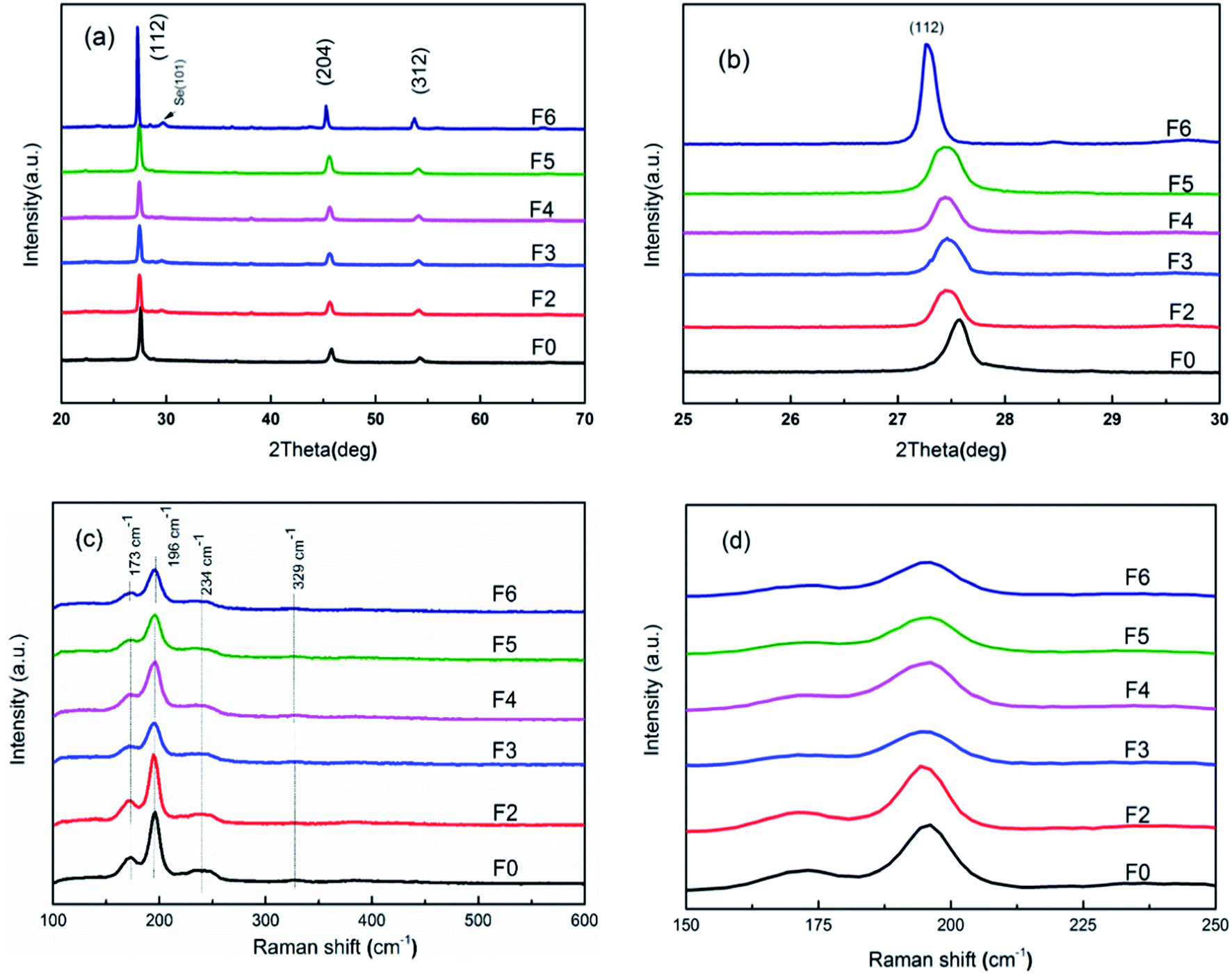 | ||
| Fig. 1 (a) X-ray diffraction patterns, (b) enlarged shifts of (112) peaks, (c) Raman spectra, and (d) enlarged view of Raman shift for the selenized (Cu1−xAgx)2ZnSn(S,Se)4 thin films with different ratios of Ag/(Ag + Cu) on the glass substrates. | ||
Fig. 2 shows the surface and cross-section SEM images of the CAZTSSe thin films on the Mo foils with x ranging from 0 to 6%. It can be seen from Fig. 2(b–d) that, the incorporation of small amount of Ag+ significantly improves the film surface morphology. As x increased from 0 to 4%, the voids and holes are obviously reduced, and the sizes of grains are clearly increased, and the grains are more densely packed. However, the surface of F6 is rough with some intergranular voids. According to the cross-section SEM images, the CAZTSSe absorber exhibits a typical tri-layer structure, i.e., a large-grained layer on top, a fine-grain layer in the middle, and a large-grained bottom layer near Mo foil. From the cross-section SEM images of the sample F6, we can see a slight reduction in the thickness of fine-grain layer and some voids generation on the surface.
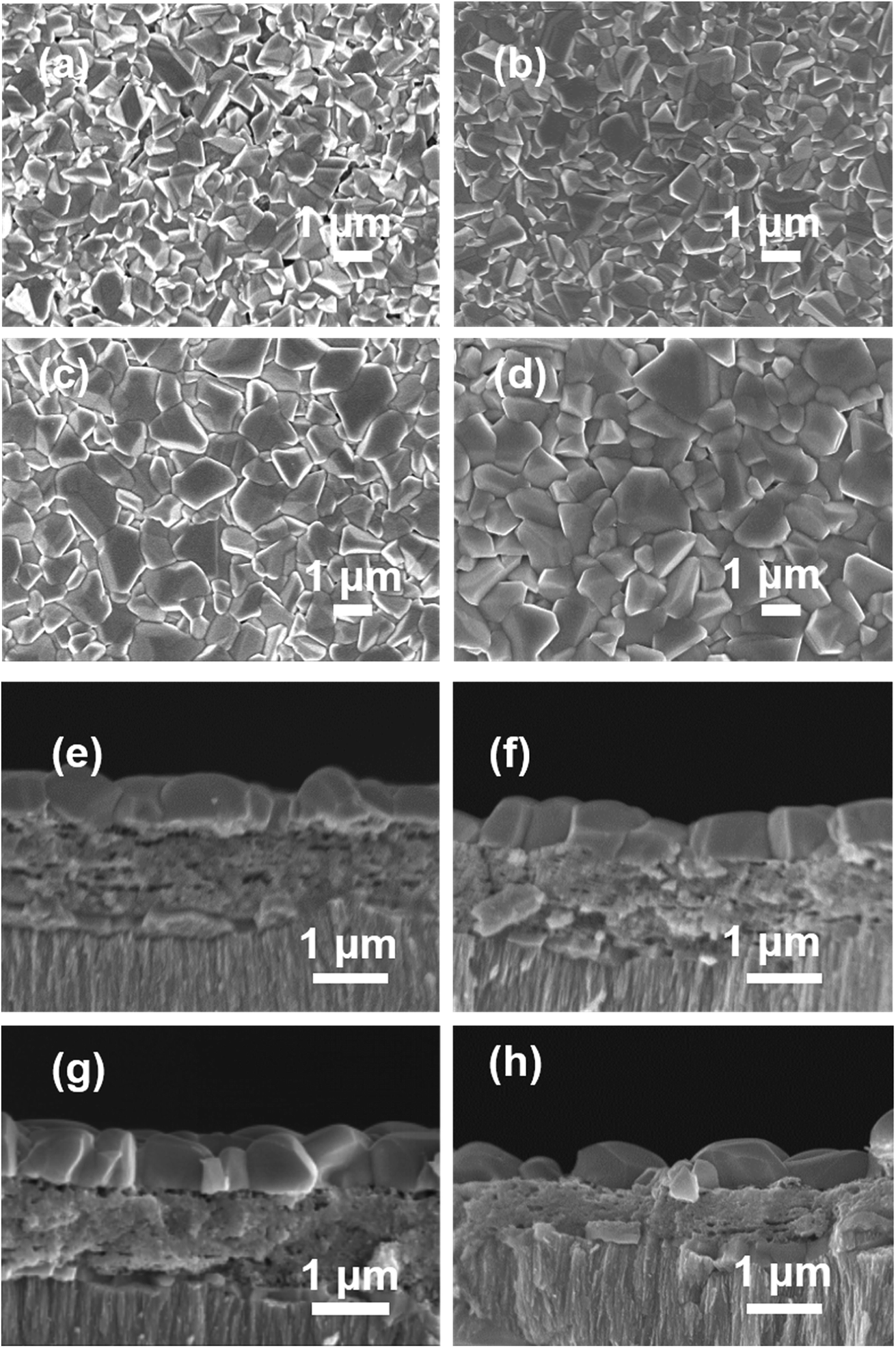 | ||
| Fig. 2 Typical surface and cross-section SEM images of the CAZTSSe thin films on the Mo foils with different ratios of Ag/(Cu + Ag): (a) and (e) F0; (b) and (f) F2; (c) and (g) F4; (d) and (h) F6. | ||
To further evaluate the impact of Ag substitution on flexible CAZTSSe solar cell performance, the current–voltage (J–V) curves of CAZTSSe solar cells fabricated with the same architecture are presented in Fig. 3(a). With x increasing from 0 to 4%, the PCE of the CAZTSSe devices on Mo foils increases from 4.34% (C0) to 6.24% (C4). As x further increases to 6%, the PCE drops to 5.01% (C6). Table 2 displays the corresponding device parameters of the samples. From Fig. 3(a) and Table 2, one can see that the photovoltaic parameters PCE, Voc, the fill factor (FF) achieve the optimized value with Ag content of 4%. Compared with the pure CZTSSe solar cell (C0), the Voc, short-circuit current density (Jsc), and FF values of the champion CAZTSSe solar cell (C4) are increased of 34 mV, 1.09 mA cm−2, and 11.33%, respectively. Fig. 3(b) displays the Voc,def of all the CAZTSSe devices. Interestingly, a severe Voc,def also decreases from 915 to 824 mV when x varies from 0 to 5%. This result indicates that the CuZn antisite defects, a primary cause of Voc loss in CZTSSe device, are obviously suppressed in the CAZTSSe samples with the optimal Ag doping level.
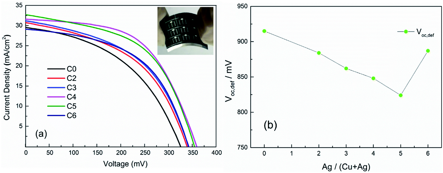 | ||
| Fig. 3 (a) Current–voltage curves of the (Cu1−xAgx)2ZnSn(S,Se)4 devices with different ratios of Ag/(Ag + Cu) under AM 1.5 G illumination. The inset shows the image of the flexible solar cell. (b) Voc,def of the (Cu1−xAgx)2ZnSn(S,Se)4 devices with different ratios of Ag/(Ag + Cu). | ||
| Sample | Ag/(Ag + Cu) | PCE (%) | Voc (mV) | Jsc (mA cm−2) | FF (%) |
|---|---|---|---|---|---|
| C0 | 0% | 4.34 | 324 | 30.42 | 43.95 |
| C2 | 2% | 4.90 | 337 | 30.64 | 47.32 |
| C3 | 3% | 5.09 | 340 | 31.09 | 48.09 |
| C4 | 4% | 6.24 | 358 | 31.51 | 55.28 |
| C5 | 5% | 6.01 | 353 | 32.65 | 52.06 |
| C6 | 6% | 5.20 | 339 | 29.22 | 50.17 |
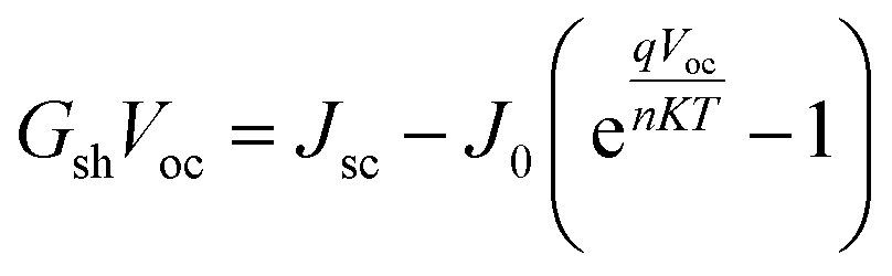
Fig. 4 shows the performance of the shunt conductance (Gsh), shunt resistance (Rsh), series resistance (Rs), diode ideality factor (A), and reverse saturation current density (J0) of the samples C4 and C0. As we all known, the relationship between the Voc and these parameters can be characterized using the following equation:23
 | (1) |
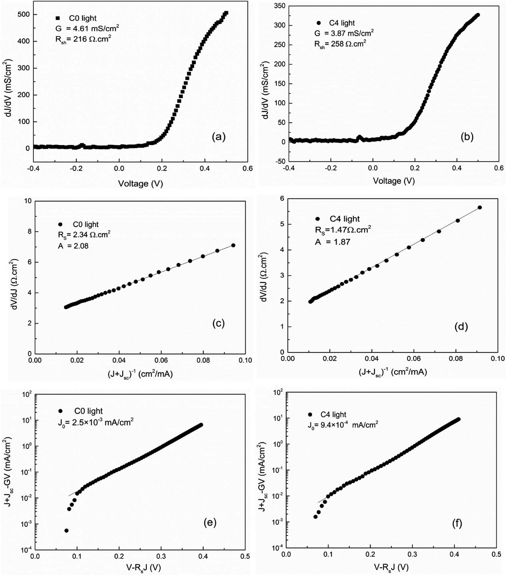 | ||
| Fig. 4 Plot of dJ/dV vs. V repainted from the standard light J–V curve for CAZTSSe samples (a) C0, (b) C4,where G value was extracted from the plateau value; Plot of dV/dJ vs. (J + Jsc)−1 for CAZTSSe samples (c) C0, (d) C4, where R and A value were evaluated from the intercept and slope of the linear region of the curve, respectively; semi-logarithmic plot of J + Jsc − GV vs. V − RJ for CAZTSSe samples (e) C0, (f) C4, where J0 value was obtained from the intercept of the curve. | ||
The reduction of the Gsh and J0 can improve the value of the Voc. In addition, Jsc and FF are also related to these parameters. Compared to sample C0, the value A of sample C4 is greatly reduced, indicating that Ag-doping can effectively alleviate the serious recombination occurred at the interface.24,25 Meanwhile, compared with sample C4, the relatively high value of J0 for sample C0 demonstrates that a mass of defects result in the carrier recombination, which will decrease the Voc and FF. Therefore, incorporating the desired amount of Ag+ into CZTSSe can effectively reduce J0 and A, and the interfaces recombination can be obviously suppressed.
Fig. 5 shows the dark and light J–V curves of samples C0 and C4. The crossover point between the dark and light J–V curves for sample C4, i.e., 22 mA cm−2, is much higher than that of sample C0, i.e., 8 mA cm−2. The crossover phenomena are mainly caused by a high density of acceptor-type defects and by the band alignment between the buffer and absorber layers.26–28 The higher value of the crossover point for CAZTSSe device implies a reduced electron supply barrier at the buffer/absorber interface, which might originate from the low density of deep acceptors close to the hetero-interface.20
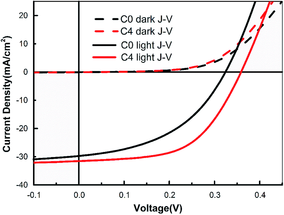 | ||
| Fig. 5 Current–voltage curves of the best flexible CAZTSSe cell and the pure CZTSSe flexible reference cell. | ||
Fig. 6(a) presents the EQE spectra of the CAZTSSe devices with x from 0 to 6%. All samples show distinct spectral response. Compared with sample C0, all samples with Ag incorporations show a higher photo-response in the visible and near-infrared wavelength. It should be noted that sample C4 shows the highest value of EQE, which is over 80% in the wavelength ranging from 540 to 790 nm, indicating a lower recombination rate of photo-generated carriers happened in the CZTSSe bulk and interface. Interestingly, the phenomenon of the low-lying decay below 520 nm has been dramatically improved compared with other experimental results by optimizing the process of CdS buffer layer.18–20 In practice, the loss of absorption results from the thicker of CdS layer. Besides, the Eg of the CAZTSSe thin film can be extracted from the data near the band edge by plotting [E × ln(1 − EQE)]2 versus E,26 as depicted in Fig. 6(b). The summary of the detailed device parameters including Voc,def (Eg/q − Voc) is also presented in Table 3. Accordingly, when the Ag content increases from 0 to 5%, the Eg values of CAZTSSe thin films decreases from 1.24 eV to a minimum of 1.12 eV and then increase to 1.23 eV for Ag content of 6%. When the Ag content increases to 5%, the Voc,def of CAZTSSe solar cells decrease to a minimum value, and when the Ag concentration is increased to 6%, the Voc,def increases again. It can be seen that, the band gap of the CAZTSSe absorber can be adjusted and the Voc,def of the flexible CAZTSSe solar cells can be ameliorated by incorporating the desired amount of Ag+.
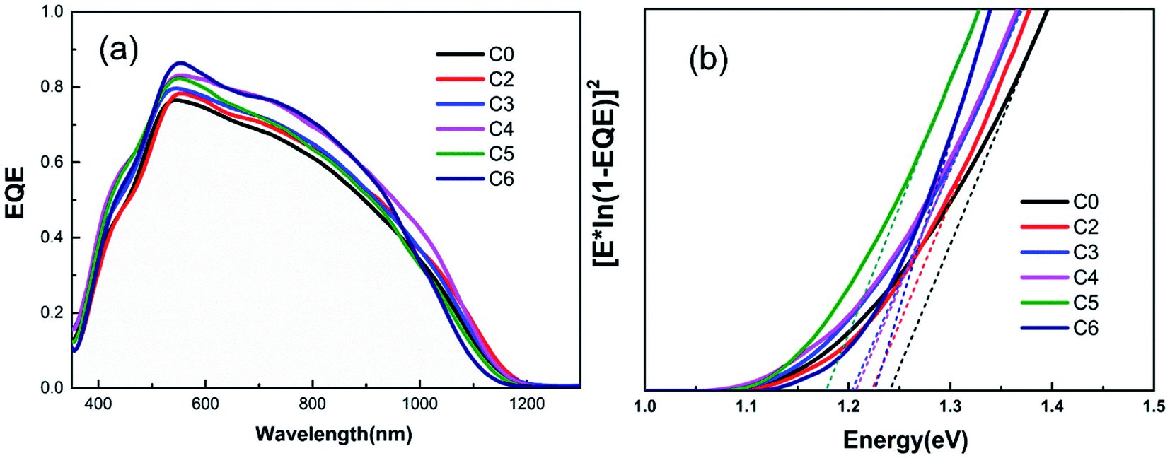 | ||
| Fig. 6 (a) Relative EQE spectra of the (Cu1−xAgx)2ZnSnSe4 thin film solar cells. (b) Band gap of the different cells determined from EQE data. | ||
| Sample | Jsc (mA cm−2) | Voc (mV) | Eg (eV) | Eg/q − Voc (mV) | PL (eV) | Eg − PL (eV) | Wd (μm) | NC–V (cm−3) |
|---|---|---|---|---|---|---|---|---|
| C0 | 30.42 | 324 | 1.239 | 915 | 1.067 | 0.172 | 0.171 | 9.05 × 10⁹ |
| C2 | 30.64 | 337 | 1.221 | 884 | 1.053 | 0.168 | 0.215 | 8.52 × 10⁹ |
| C3 | 31.09 | 340 | 1.202 | 862 | 1.039 | 0.163 | 0.236 | 7.86 × 10⁹ |
| C4 | 31.51 | 358 | 1.206 | 848 | 1.046 | 0.160 | 0.299 | 6.68 × 10⁹ |
| C5 | 32.65 | 353 | 1.177 | 824 | 1.028 | 0.149 | 0.262 | 7.55 × 10⁹ |
| C6 | 29.22 | 339 | 1.225 | 887 | 1.052 | 0.161 | 0.202 | 8.62 × 10⁹ |
Fig. 7(a) depicts the normalized photoluminescence (PL) spectra as a function of the Ag/(Ag + Cu) in the CAZTSSe thin films. PL spectroscopy is a useful technique to estimate the band gap of the surface layer (depth below 50 nm) for direct band gap materials, and the results are illustrated in Table 3 and Fig. 7(b). It can be seen that the room-temperature PL peak position shifts to lower energies, i.e., it decreases from 1.07 to 1.03 eV as Ag content increased from 0 to 5%, and it shifts to a higher value (1.05 eV) when the Ag content is increased to 6%. This observation suggests that there is a turning point in the curve of Eg vs. Ag concentration, which explains the controversial observation of previous works, i.e., it is reported in ref. 17, 18 and 20 that the band gap increases with the ratio of Ag/(Ag + Cu), but it is found in ref. 19 that the band gap decreases with the ratio of Ag/(Ag + Cu). Besides, the results are in good agreement with the Eg obtained from the EQE. It can be seen from Fig. 7(c) that, as the Ag concentration x is increased from 0 to 5%, the energy differences between the Eg and the PL peak position is decreased from 172 to 149 meV. The results indicate that the band tailing can be effectively reduced by introducing appropriate Ag concentration into CZTSSe.
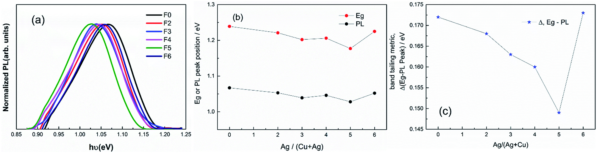 | ||
| Fig. 7 (a) Normalized PL spectra of (Cu1−xAgx)2ZnSnSe4 thin films with different x (x = 0–6%). (b) Eg values, room-temperature PL peak positions and Voc,def as a function of Ag/(Ag + Cu). (c) Energy differences between the room-temperature band gap and PL peak position with different x (x = 0–6%). | ||
In order to find out the reason of the different performances, the depletion region width (Wd) and charge carrier density (NC–V) of the samples were measured by a C–V method at a reverse bias from 0 to −1 V at 300 K, and the results are depicted in Fig. 8(a) and (b). The detailed values of Wd and NC–V for the CAZTSSe devices with different x are shown in Table 3. It can be seen that, the NC–V decreases from 9.05 × 10¹⁶ to 6.68 × 1016 cm−3 when x increases from 0 to 4%, and the NC–V is increased to 8.62 × 1016 cm−3 when x is further increased to 6%. This indicates that the incorporation of Ag will greatly influence the NC–V of the absorber and influence the Wd of the CAZTSSe devices. With x varying from 0 to 4%, the Wd of the devices increases from 0.17 μm to the maximum value of 0.30 μm. However, as the Ag content increased from 4 to 6%, the Wd of the device decreases to 0.20 μm. It is well known that Wd can influence the charge separation and collection, and finally affect the conductivity of solar cells.29 A narrow depletion region width is harmful for the effective collection of the photo-generated charge carrier, especially for the long wavelength region close to the band edge, and can result in increased interface recombination or tunneling recombination, thus leading to a significant Voc loss. Our work suggests that the substitution of Cu+ with Ag+ in CZTSSe thin film solar cell can significantly increase the Wd value for the optimal Ag composition (x = 4%). As a result, the Voc and FF are successfully increased from 324 mV, 43.95% to 358 mV, 55.28%, respectively. The above results prove that both of the charge carrier concentration and Wd are very sensitive to the relative content of Ag+, and the optimal incorporation of Ag (x = 4%) can significantly increases the value of Wd.
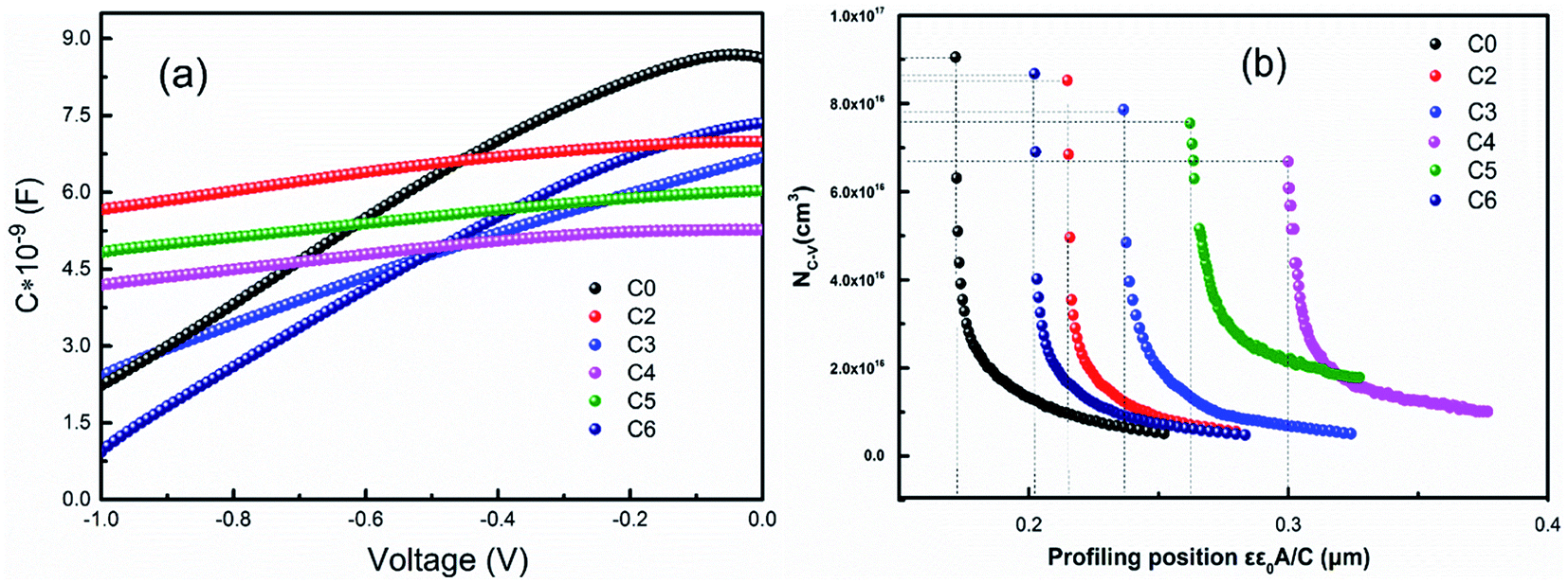 | ||
| Fig. 8 (a) Capacitance–voltage (C–V) curves of (Cu1−xAgx)2ZnSnSe4 thin film solar cells with different x. (b) Space-charge density and depletion width derived from C–V curves. These results were obtained under reverse bias from −1.0 to 0 V at 300 K. | ||
4. Conclusion
In conclusion, a safe and convenient solution method has been developed to produce CAZTSSe thin films on Mo foils. The small quantity of Ag+ incorporation can be easily controlled by adjusting the chemical composition of the elemental powders. The band gap of CAZTSSe thin films can be tuned to a minimum value when the Ag content is increased to 5%, and the band gap increases when the Ag concentration is further increased to 6%. Meanwhile, increasing Ag content in the absorber will lead to better crystallization of the CZTSSe thin films, and suppressed the recombination at the interfaces. Finally, a conversion efficiency up to 6.24% is achieved for the flexible CAZTSSe solar cell with 4% Ag incorporation. Comparing with the pure flexible CZTSSe solar cell, about 67 mV reduction in voltage deficit occurs as a result of Ag substitution, which contributes to the improvement of the device performance.Conflicts of interest
There are no conflicts to declare.Acknowledgements
This work was supported by the National Natural Science Foundation of China (No. 61574038).References
- D. Tiwari, T. Koehler, X. Lin, R. Harniman, I. Griffiths, L. Wang, D. Cherns, R. Klenk and D. J. Fermin, Chem. Mater., 2016, 28, 4991–4997 CrossRef.
- Y. Yang, G. Wang, W. Zhao, Q. Tian, L. Huang and D. Pan, ACS Appl. Mater. Interfaces, 2015, 7, 460–464 CrossRef PubMed.
- D. B. Mitzi, O. Gunawan, T. K. Todorov and D. A. R. Barkhouse, Philos. Trans. R. Soc., A, 2013, 371, 20110432 CrossRef PubMed.
- F. Jiang, S. Ikeda, T. Harada and M. Matsumura, Adv. Energy Mater., 2014, 4, 1301381 CrossRef.
- D. B. Mitzi, O. Gunawan, T. K. Todorov, K. Wang and S. Guha, Sol. Energy Mater. Sol. Cells, 2011, 95, 1421–1436 CrossRef.
- G. Wang, W. Zhao, Y. Cui, Q. Tian, S. Gao, L. Huang and D. Pan, ACS Appl. Mater. Interfaces, 2013, 5, 10042–10047 CrossRef PubMed.
- W. Wang, M. T. Winkler, O. Gunawan, T. Gokmen, T. K. Todorov, Y. Zhu and D. B. Mitzi, Adv. Energy Mater., 2014, 4, 1301465 CrossRef.
- K. W. Brew, S. M. McLeod, S. M. Garner and R. Agrawal, Thin Solid Films, 2017, 642, 110–116 CrossRef.
- L. Dong, S. Cheng, Y. Lai, H. Zhang and H. Jia, Thin Solid Films, 2017, 626, 168–172 CrossRef.
- J. Xu, Z. Cao, Y. Yang and Z. Xie, J. Mater. Sci.: Mater. Electron., 2014, 26, 726–733 CrossRef.
- Y. Zhang, Q. Ye, J. Liu, H. Chen, X. He, C. Liao, J. Han, H. Wang, J. Mei and W. Lau, RSC Adv., 2014, 4, 23666–23669 RSC.
- S. Yazici, M. A. Olgar, F. G. Akca, A. Cantas, M. Kurt, G. Aygun, E. Tarhan, E. Yanmaz and L. Ozyuzer, Thin Solid Films, 2015, 589, 563–573 CrossRef.
- S. Chen, A. Walsh, X.-G. Gong and S.-H. Wei, Adv. Mater., 2013, 25, 1522–1539 CrossRef PubMed.
- J. Li, H. Wang, L. Wu, C. Chen, Z. Zhou, F. Liu, Y. Sun, J. Han and Y. Zhang, ACS Appl. Mater. Interfaces, 2016, 8, 10283–10292 CrossRef PubMed.
- D. Shin, B. Saparov and D. B. Mitzi, Adv. Energy Mater., 2017, 7, 1602366 CrossRef.
- Z.-K. Yuan, S. Chen, H. Xiang, X.-G. Gong, A. Walsh, J.-S. Park, I. Repins and S.-H. Wei, Adv. Funct. Mater., 2015, 25, 6733–6743 CrossRef.
- T. Gershon, Y. S. Lee, P. Antunez, R. Mankad, S. Singh, D. Bishop, O. Gunawan, M. Hopstaken and R. Haight, Adv. Energy Mater., 2016, 6, 1502468 CrossRef.
- C. J. Hages, M. J. Koeper and R. Agrawal, Sol. Energy Mater. Sol. Cells, 2016, 145, 342–348 CrossRef.
- Y. Qi, Q. Tian, Y. Meng, D. Kou, Z. Zhou, W. Zhou and S. Wu, ACS Appl. Mater. Interfaces, 2017, 9, 21243 CrossRef PubMed.
- X. H. Yun Zhao, B. Xu, W. Li, J. Li, J. Li, M. Wang, C. Dong, P. Ju and J. Li, IEEE J. Photovolt., 2017, 7, 874–881 Search PubMed.
- R. Zhang, S. M. Szczepaniak, N. J. Carter, C. A. Handwerker and R. Agrawal, Chem. Mater., 2015, 27, 2114–2120 CrossRef.
- A. Khare, B. Himmetoglu, M. Johnson, D. J. Norris, M. Cococcioni and E. S. Aydil, J. Appl. Phys., 2012, 111, 3–645 Search PubMed.
- G. Yang, Y.-F. Li, B. Yao, Z.-H. Ding, R. Deng, H.-F. Zhao, L.-G. Zhang and Z.-Z. Zhang, J. Phys. D: Appl. Phys., 2018, 51, 105103 CrossRef.
- G. Brammertz, M. Buffiere, S. Oueslati, H. ElAnzeery, K. Ben Messaoud, S. Sahayaraj, C. Koeble, M. Meuris and J. Poortmans, Appl. Phys. Lett., 2013, 103, 163904 CrossRef.
- H. Y. Park, D. G. Moon, J. H. Yun, S. K. Ahn, K. H. Yoon and S. Ahn, Appl. Phys. Lett., 2013, 103, 894–897 Search PubMed.
- A. Niemegeers, M. Burgelman, R. Herberholz, U. Rau, D. Hariskos and H. W. Schock, Prog. Photovoltaics, 1998, 6, 407–421 Search PubMed.
- M. Burgelman, F. Engelhardt, J. F. Guillemoles, R. Herberholz, M. Igalson, R. Klenk, M. Lampert, T. Meyer, V. Nadenau and A. Niemegeers, Prog. Photovoltaics, 1997, 5, 121–130 Search PubMed.
- S. S. Hegedus and W. N. Shafarman, Prog. Photovoltaics, 2004, 12, 155–176 Search PubMed.
- Y.-F. Qi, D.-X. Kou, W.-H. Zhou, Z.-J. Zhou, Q.-W. Tian, Y.-N. Meng, X.-S. Liu, Z.-L. Du and S.-X. Wu, Energy Environ. Sci., 2017, 10, 2401–2410 RSC.
| This journal is © The Royal Society of Chemistry 2018 |