
 Open Access Article
 This Open Access Article is licensed under a Creative Commons Attribution-Non Commercial 3.0 Unported Licence
Dual function of molybdenum sulfide/C-cloth in enhancing the performance of fullerene nanosheets based solar cell and supercapacitor†
Aparajita Dasa,
Melepurath Deepa *a and
Partha Ghosalb
*a and
Partha Ghosalb
aDepartment of Chemistry, Indian Institute of Technology Hyderabad, Kandi-502285, Sangareddy, Telangana, India. E-mail: mdeepa@iith.ac.in
bDefence Metallurgical Research Laboratory, DRDO, Hyderabad 500058, Telangana, India
First published on 12th October 2018
Abstract
Quantum dot solar cells (QDSCs) with hexagonal fullerene nanosheets (C60-NS) embedded in a titanium oxide/cadmium sulfide (TiO2/CdS) photoanode coupled with a carbon-cloth (C-cloth) coated with molybdenum sulfide (MoS2) counter electrode (CE) are studied for the first time. C60-NS due to a favorable work function of 4.57 eV and a conductance of 1.44 μS, enable faster electron injection from the conduction band of cadmium sulfide to the current collector, in contrast to the bulk fullerene based TiO2/CdS solar cell. The champion cell with the TiO2/C60-NS/CdS photoanode and a MoS2/C-cloth CE exhibits a high power conversion efficiency of 5.6%, greater by ∼14% relative to its' analogue cell with bulk fullerene. A large area cell of 1 cm2 dimensions with TiO2/C60-NS/CdS gives a PCE of 2.9%. The effect of MoS2 in improving the efficiency of the cell with a TiO2/C60-NS/CdS photoanode is realized in terms of enhanced electrocatalytic activity for polysulfide reduction, and lower charge transfer resistance at the polysulfide/CE interface compared to a cell with the same photoanode but having pristine carbon-cloth as the CE. The ability of MoS2 for catalyzing the oxidized polysulfide species at the CE and C60-NS for improving the charge collection at the photoanode serve as indicators for their wider utilization in solar cells. It also serves as a good supercapacitor material. A MoS2/C-cloth based symmetric cell exhibits a specific capacitance of 645 F g−1 at 2 A g−1, which shows its' potential for energy storage as well. By integrating the QDSC and the supercapacitor, the resulting integrated device acquires a photovoltage of 0.7 V, under 1 sun illumination.
1. Introduction
In recent years, quantum dot solar cells (QDSCs) have scaled very high power conversion efficiencies, greater than 12%,1,2 thus propelling them to the forefront of photovoltaic (PV) research. Quantum dots (QDs) are characterized by band gap tunability, multiple exciton generation, low cost and high extinction coefficient; the former three properties are not available to Ru-dyes typically used in dye sensitized solar cells (DSSCs), the analogues of QDSCs.3 These benefits of QDs provide the impetus to apply them in PV cells. Among the various visible and/or near infrared (NIR) light absorbing QDs, such as CdS,4 CdSe,5 PbS6 and CuInS2,7 which have been used in QDSCs in the past, CdS QDs absorb the blue-green region of the solar spectrum, they are cheap, and films of CdS can be easily deposited over the wide gap semiconductor (TiO2) by using simple methods at room temperature, without any expensive equipment or complex reaction conditions of temperature or pressure or inert atmosphere. Charge collection at the photoanode is improved by the use of passivation layers like ZnS, ZnSe, SiO2, and amorphous a-TiO2, and their combinations.8–10 These layers reduce charge recombination between photoanode and electrolyte and within the photoanode. Zhong's group achieved a PCE of 9.48% for CdSeTe/CdS quantum dot solar cells by applying a passivation layer of SiO2 and a-TiO2.11 Recently, for a cell with alloyed Cu–In–Ga–Se QDs coated with a ZnS and SiO2 barrier layer, a high PCE of 11.6% was achieved with a titanium mesh/carbon based counter electrode (CE).12 Besides the use of passivation layers, other strategies adopted in PV literature involve the incorporation of electrically conducting carbonaceous nanostructures such as graphene,13 fullerene (C60),14 carbon nanotubes (CNTs)15 in the photoanode, to increase electron transport, minimize recombination and improve photocurrents. Fullerene, due to a high carrier mobility and a work function of 4.3 eV,16 is widely used as an electron acceptor in organic photovoltaic cells,17 and therefore it can be applied to photoanodes of QDSCs as well, to promote electron transport to the current collector.14In addition to the photoanode, CE is a vital component of a QDSC. It collects electrons from external circuit and catalyzes the reduction of oxidized species of the polysulfide electrolyte, during cell operation. An ideal CE should be cost effective, electrically conductive, chemically stable and electrocatalytically active. Carbonaceous materials such as carbon, CNT and RGO etc., metal sulfides and selenides are observed to fulfil these requirements, and have been used in QDSCs in the past.18–24
Among metal chalcogenides, Cu2S is the most commonly used CE catalyst for polysulfide reduction, due to its' high electrocatalytic activity and chemical stability, but one of the objectives in this study is to prepare and use an equally effective alternate CE, that can also double up as an supercapacitor electrode. MoS2, satisfies these pre-requisites. While MoS2 is shown to be a powerful electrocatalyst for hydrogen production,25 it has been used rarely as a CE in QDSCs26 and DSSCs.27 It is relatively less explored as a CE in QDSCs, compared to the exhaustively studied Cu2S. It also shows good catalytic activity for polysulfide reduction, and is very stable in the polysulfide electrolyte. It is also easily processable in the form a uniform coating over the current collector (C-cloth), through a direct one-pot, in situ preparation cum deposition method. This method establishes a strong ohmic contact between MoS2 and C-cloth, and therefore electron delivery to MoS2 and electron extraction from MoS2 are rendered facile, during charge–discharge process, in the supercapacitor. Furthermore, MoS2 is capable of storing and releasing charge through an electrical double layer mechanism and a faradaic redox reaction. The structure of MoS2 is composed of three atom layers: a Mo layer sandwiched between two S layers, and the triple layers are stacked repetitively and held together by van der Waal's forces. The layered structure of MoS2 furnishes a large number of accessible electrochemically active sites, which maximizes the ion ingress from the electrolyte during charging. Due to the aforementioned reasons, MoS2 is chosen to be the CE, in this report.
Tai et al., demonstrated a DSSC with a CE composed of a few layers of MoS2-nanosheets (NS) anchored on multiwalled carbon nanotubes (MWCNTs) with high electrical conductivity and electrocatalytic activity, and the corresponding PCE was 6.45%.28 Seol et al., used a Mo-compound/CNT-graphene composite based CE in a QDSC, and a PCE of 5.41% was achieved.29 MoS2 besides being used as a CE in solar cell, is also widely used in supercapacitors as an energy storage electrode, due to its high surface area, high electrical conductivity and high storage capacity. Ma et al., reported a poly(pyrrole)/MoS2 nanocomposite based supercapacitor and it showed a high specific capacitance of 553.7 F g−1 at a current density of 1 A g−1.30 Huang et al., synthesized poly(aniline)/MoS2 which gave a specific capacitance of 575 F g−1 at 1 A g−1.31 They also developed a layered MoS2–graphene composite, which showed a capacitance of 243 F g−1 at a discharge current density of 1 A g−1.32 The performance was attributed to a 3D MoS2–graphene interconnected conductive network which promotes not only efficient charge transport and facilitates electrolyte diffusion, but also prevents effectively the volume expansion/contraction and aggregation of electroactive materials during the charge–discharge process.
Here, we report the fabrication and characterization of a QDSC with a TiO2/C60-NS/CdS photoanode, a MoS2/carbon (C)-cloth CE and a polysulfide gel as the hole transport layer. C60-NS are prepared by liquid–liquid interfacial precipitation method and anchored to the TiO2 layer, and CdS QDs are deposited by successive ionic layer adsorption and reaction (SILAR). The role of the C60-NS in ameliorating charge transfer and transport is studied by comparing the cell with control cells with TiO2/C60-B (bulk)/CdS/ZnS and TiO2/CdS/ZnS photoanodes. The role of MoS2 in improving cell performance is evaluated by comparing cell configurations having the same photoanode, but different CEs: pristine C-cloth and MoS2/C-cloth. Based on the findings reported here, MoS2 and C60-NS can be applied to other cell configurations for improving cell response. The ability of MoS2/C-cloth to function as an energy storage material is also explored, by studying its' capacitive characteristics. In addition, the performance of an integrated device comprising of an electrically connected QDSC and the supercapacitor are presented.
2. Experimental
2.1 Chemicals
TiO2 P25 powder was a free gift from Evonik. Cadmium acetate (Cd(CH3COO)2), sodium sulfide (Na2S), fullerene (C60), molybdenum oxide (MoO3), thioacetamide, methanol, isopropanol and acetyl acetone were procured from Aldrich. Ammonium fluoride (NH4F), carbon tetrachloride (CCl4), ethanol, acetone, titanium tetrachloride (TiCl4), oleic acid, Triton X-100 were obtained from Merck. Fluorine-doped tin oxide coated glass substrates (FTO, resistivity ∼15 Ω sq−1) were obtained from Pilkington. Deionized water with a resistivity of ∼18.2 MΩ cm was obtained from a Millipore Direct-Q3 UV system. C-cloth with a sheet resistance of 10 Ω cm−2 was procured from Alibaba Pvt. Ltd. Fumed silica (SiO2) was a free gift from Cabot Corporation.2.2 Synthesis of C60 nanosheets and photoanode(s) fabrication
C60-NS were prepared by using liquid–liquid interfacial precipitation method reported by Sathish et al.33 0.1 g of C60 powder was dissolved in 25 mL of CCl4 followed by ultrasonication for 30 min and a purple colored solution was obtained. Then the final solution was filtered to remove the undissolved C60 powder. 1 mL of the C60 saturated solution was taken in a clean glass vial and kept in an ice water bath, maintaining temperature to 5 °C. In a separate vial, 6 mL of isopropyl alcohol (IPA) was taken and maintained at the same temperature. When both solutions were in 5 °C, IPA was added slowly to the C60 solution. The mixture was kept for 5 min at 5 °C without any disturbance. It was ultrasonicated for 5 min and then stored in 5 °C for 24 h. The color of the solution was pale yellow color, which signaled the formation of C60-nanosheets (NS). This solution was directly used for preparing films. C60-bulk (B) solution was prepared by adding 6 mL of CCl4 solvent to 1 mL of the C60 saturated solution.Over a cleaned FTO film, a TiO2 paste was applied by doctor blade method. TiO2 paste was prepared by dispersing TiO2 powder in a solution of acetyl acetone (1.5 mL), deionized water (8.5 mL) and Triton-X 100 (20 mg) followed by sonication for 15 min. It was applied on FTO, dried for 30 min at 60 °C in oven and annealed for 30 min at 500 °C. One more layer was applied using the same process. The TiO2 film was immersed in a 0.04 M aqueous TiCl4 solution, maintained at 70 °C for 30 min and rinsed in a deionized water followed by annealed at 500 °C for 30 min to obtain the final layer.
A solution of C60-NS (0.57 mg in 1 mL) was drop cast on a TiO2/FTO film and rinsed in a CCl4/IPA solvent mixture and dried at ambient temperature. The same procedure was used for coating the C60-B solution over a TiO2/FTO film. Then, CdS QDs were deposited on a TiO2/C60-NS film by the SILAR method. The film was immersed in a beaker containing 0.1 M cadmium acetate/methanol for 2 min, rinsed in methanol and dried for 2 min and then immersed in another beaker containing 0.1 M sodium sulfide/methanol for 2 min, rinsed in methanol and dried for 2 min. Thus, one cycle of deposition was completed. The film was subjected to six more SILAR cycles to obtain a TiO2/C60-NS/CdS film, which was stored at 45 °C in an oven in dark. Also, a TiO2/C60-B/CdS film were fabricated by depositing CdS using 7 cycles of SILAR. Then 2 layers of ZnS were applied by immersing the photoanode in a 0.1 M zinc acetate/methanol solution for 2 min, followed by a methanol rinse and dried for 2 min and then in a 0.1 M Na2S/methanol solution for 2 min, rinsed in methanol and dried for 2 min.
2.3 Counter electrode
Two electrodes: carbon (C)-cloth and MoS2/C-cloth were used as CEs. MoS2/C-cloth was prepared by an in situ hydrothermal method reported by Yu et al.34 In a beaker, 30 mg of MoO3, 45 mg of thioacetamide and 300 mg of ammonium fluoride (NH4F) were taken and 30 mL of distilled water was added and it was stirred vigorously for 30 min. The mixture solution was transferred to a 60 mL Teflon-lined stainless steel autoclave and a C-cloth (area: 6 cm2) was kept immersed in it and this assembly was heated in an oven at 200 °C for 8 h. The autoclave was cooled down to room temperature. The MoS2/C-cloth was washed in distilled water and ethanol respectively and dried at 60 °C in a vacuum oven and stored at 45 °C in an oven in dark, prior to use. The mass loading amount of MoS2 on C-cloth is 1 mg.QDSCs were constructed by assembling a photoanode (TiO2/C60-NS/CdS or TiO2/C60-B/CdS or TiO2/CdS), a CE (C-cloth or MoS2/C-cloth) and a polysulfide gel electrolyte (composed of 1 M Na2S and 1 M S dissolved in deionized water and 5% fumed silica dispersed therein) in a sandwich configuration. A parafilm spacer was also used to prevent shorting. The cells were illuminated from the rear side for all experiments involving irradiance. The active area of the exposed photoanode was maintained between 0.1 cm2.
2.4 Characterization techniques
Raman spectra of pristine C60 and C60-NS were recorded on a Bruker Senterra dispersive Raman microscope spectrometer, having a 532 nm laser excitation source. X-ray diffraction (XRD) patterns of pristine C60, C60-NS, MoS2 were recorded on a PANalytical, X'PertPRO instrument with a Cu-Kα (λ = 1.5406 Å) radiation. TEM analysis was performed using a Jeol 2100 microscope (200 kV) and samples were directly transferred onto carbon-coated copper grids. Surface morphology of C60-NS was examined under a scanning electron microscope (Zeiss Evo 18 Special Edition). Optical absorption spectra of solutions were measured in absorbance mode and films in diffuse reflectance mode on a UV-Vis spectrophotometer (T90+, PG Instruments). A Horiba Flouromax-4 fluorescence spectrometer was used to measure the fluorescence spectra of electrodes. Emission lifetime was deduced by time-correlated single photon counting (TCSPC) method, using a Horiba Jobin Yvon data station HUB functioning in the TCSPC mode. A nano LED diode was employed as an excitation source having emission pulses at 370 nm with 1 MHz repetition rate and a pulse duration of 1.3 ns. A Ludox solution (colloidal silica) was used as a prompt to acquire the instrument response function. Current versus potential data of QDSCs were measured using a LOT-Oriel Xe arc lamp, which gave an irradiance of 1 sun (100 mW cm−2, AM 1.5, coupled with an Autolab PSTAT 302N electrochemical workstation). Light irradiance was measured using a Newport power meter. Cyclic voltammetry, Linear sweep voltammetry plots for the photoactive electrodes and electrochemical impedance spectra (EIS, at an ac amplitude of 20 mV over a frequency range of 1 MHz to 0.1 Hz) were recorded on the same workstation. External quantum efficiency (EQE) versus wavelength spectra were recorded by employing a quantum efficiency measurement system, Oriel IQE-200, capable of measurements compliant to ASTM E1021-06 which was equipped with a quartz tungsten halogen lamp as a light source. KPFM (Kelvin probe force microscopy) (Veeco, Multimode 8 with ScanAsyst and Nanoscope 8.10 software) was used for recording topography and surface potential images. A Co/Cr tip with a Sb doped Silicon cantilever was used as probe with a radius of 10 nm, a spring constant of 0.2 N cm−2 and a current sensitivity of 1 nA V−1. Between the tip and sample, a load force of 50 nN was maintained. The sample/FTO glass was affixed on a stainless steel disk with a conducting carbon tape and a silver paste was used for taking contacts. An ac bias of 5 V was applied between sample and probe and a modulated force was measured between them using a cantilever for recording the surface potential map. Until the oscillation dropped to zero (when applied Vdc equaled to VCPD i.e., the contact potential difference) KPFM feedback adjusted a dc bias. In the first pass, a topography map was obtained in tapping mode and a surface potential map was measured in the second pass.3. Results and discussion
3.1 Structural studies
The transmission electron microscopy (TEM) images of the C60-NS and the TiO2/C60-NS/CdS film are shown in Fig. 1 (a–f). C60-NS show overlapping hexagonal semi-crystalline nanosheets, which are formed at the CCl4-IPA interface (Fig. 1a). Along with the hexagonal nanosheets (NS), particles of other geometric shapes are also observed. This may be due to the aggregation of nanosheets. The edges of a hexagonal sheet are seen in an enlarged view in Fig. 1b. The size of nanosheets lies in the range of 200–500 nm. Fig. 1c shows the selected area electron diffraction (SAED) pattern of a C60-NS, where bright spots are superimposed over concentric diffuse rings. The spots are indexed to the (004) and (006) planes of C60, which correspond to d = 3.18 and 2.75 Å of the hexagonal structure of fullerene (powder diffraction file (PDF): 470787); this is clearly indicative of the sheet like structure of C60, because C60-B has a fcc structure (seen later through diffraction studies), and C60-NS are hexagonal. The images of the TiO2/C60-NS/CdS film (Fig. 1d and e) show TiO2 nanoparticles (seen as large aggregated particles of irregular shapes, 20–50 nm in dimensions) and CdS QDs (visible as small particles, 5–10 nm in dimensions) juxtaposed with the C60-NS, which are seen in the form of hexagonal shapes. From the image in Fig. 1e, the hexagonal shape of the C60-NS in dark contrast is obvious. The SAED pattern (Fig. 1f) shows bright spots that correspond to the lattice planes from the crystal structures of the different components of the photoanode. TiO2 produced spots corresponding to hkl = (004), (200) and (105) planes of the body centered tetragonal structure (PDF: 894921), corresponding to d = 2.37, 1.9, 1.67 Å. CdS produces spots due to hkl = (111) and (311) corresponding to d = 3.35 and 1.77 Å of the face centered cubic (fcc) lattice of CdS (PDF: 652887), and spot due to the (006) plane of hexagonal structured C60 is also observed. These sheets are formed by the liquid–liquid interfacial pressure.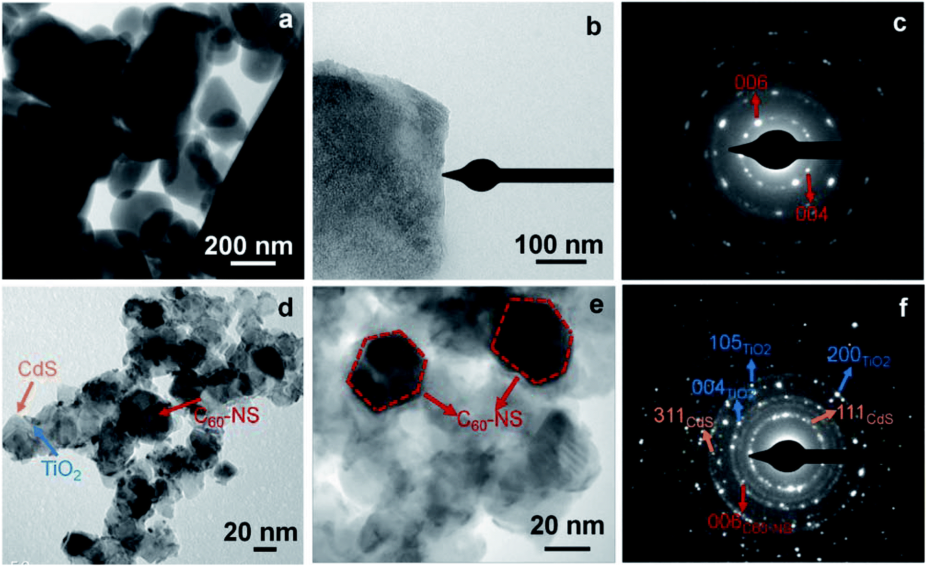 | ||
| Fig. 1 (a and b) TEM images of C60-NS with (c) the corresponding SAED pattern, (d and e) TEM images of TiO2/C60-NS/CdS film with (f) the corresponding SAED pattern. | ||
XRD patterns of C60-B, C60-NS, MoS2 and C-cloth deposited on micro-slide glass substrates are shown in Fig. 2a and b and S2.† Bulk fullerene (C60-B) shows peaks at 2θ = 10.73, 17.57, 20.64, 21.57, 27.23, 27.96, 30.7 and 32.6° with corresponding d spacings of 8.28, 5.06, 4.3, 4.11, 3.39, 3.2, 2.91 and 2.75 Å that match with (111), (220), (311), (222), (331), (024), (422) and (333) planes respectively of face centered cubic (fcc) lattice of C60 (PDF: 820505) (Fig. 2b). C60-NS shows peaks at 2θ = 10.8, 17.7, 20.75, 21.62, 28.06, 30.83 and 32.68° that correspond to d spacings of 8.19, 5, 4.27, 4.11, 3.18, 2.9 and 2.75 Å, aligning with the (002), (110), (112), (004), (114), (300) and (006) planes of a hexagonal primitive structure of C60 (PDF: 470787) (Fig. 2a).
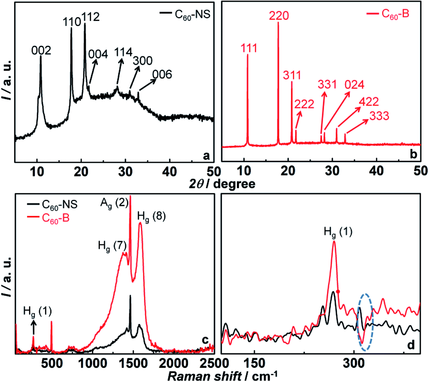 | ||
| Fig. 2 (a and b) XRD patterns of C60-NS and C60-B, (c) Raman spectra of C60-NS and C60-B, (d) shows the enlarged view of Raman spectra in 100–400 cm−1 range. | ||
3.2 Comparison of C60-NS and C60-B
Fig. 2c shows the Raman spectra of C60-NS and C60-B measured in wavenumber range of 50–2500 cm−1 respectively. A peak at 270 cm−1 is due the Hg (1) squashing mode of C60. Peaks at 1415 and 1575 cm−1 are attributed to the Hg (7) and Hg (8) modes of C60. In addition, two strongest Raman lines at 493.8 and 1464 cm−1 are assigned to the two symmetric modes of Ag (1) and Ag (2) corresponding to the double-bond stretching “pentagonal pinch” mode and the “breathing” mode.35 The pentagonal pinching mode of Ag (1) is susceptible to intermolecular interaction. It is noted that in C60-NS, the Hg (1), Hg (7) and Hg (8) modes are shifted to lower frequencies. It may be attributed to the photo-reaction between the excited C60 and a neighbouring molecule during laser irradiation.36 An additional peak was observed at 308.3 cm−1 for C60-NS that was not seen for C60-B. A peak at 270 cm−1 was split into two peaks showing a high degree of crystallinity present in C60-NS (Fig. 2d).Fig. 3a, c and b, d show the topography and surface potential maps of C60-NS and C60-B deposited as thin films on FTO/glass substrates. During the measurement, a Co/Cr tip of a known work function (φ) was held at a height of 100 nm from the sample surface. The conducting tip scans the sample surface and electrons are transferred between the two until the Fermi levels (EF) align. The tip maps the topography of the sample in the tapping mode in the first pass and it maps the contact potential difference or surface potential (VCPD) as a function of the lateral coordinate in the second pass. The conducting tip was calibrated with highly ordered pyrolytic graphite (HOPG) of a known work function of 4.6 eV. For HOPG, the VCPD was 90 mV. Thus, the work function of an unknown sample is determined by the equation.
| φsample = 4.6 eV + VCPD(HOPG) − VCPD(sample) | (1) |
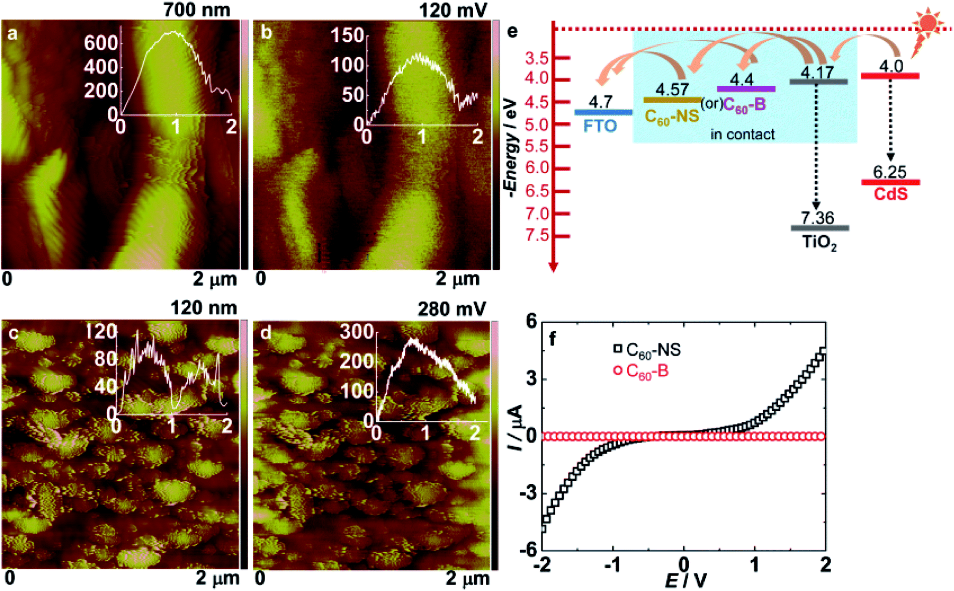 | ||
| Fig. 3 (a, c) and (b, d) are topography and surface potential maps of C60-NS and C60-B obtained from KPFM, and (e) energy band diagram of TiO2/C60-NS/CdS electrode showing the electron transfer modes, (f) linear sweep voltammetry plots of C60-NS and C60-B. | ||
Hence, the work function of C60-NS is calculated to be 4.57 eV by using VCPD = 120 mV, whereas the work function of C60-B is calculated to be 4.4 eV by using VCPD = 280 mV respectively. According to literature, the work function of pristine fullerene is ∼4.3 eV which is in agreement with the calculated value.16 The CB of CdS is poised at 4 eV (Fig. S1b, ESI†) and therefore, excited electrons upon illumination, can easily cascade into C60-B or C60-NS, via TiO2, which has a CB at 4.17 eV (Fig. S1a, ESI†). It must be recalled from the deposition method that TiO2 has a porous matrix and it is in direct contact with C60-B or C60-NS. From the C60-B or C60-NS, the electrons are relayed to the current collector (FTO), which has a work function of 4.7 eV (Fig. 3e). The higher magnitude of energy level gradient between the CB of TiO2, and ϕ (C60-NS) compared to that between the CB of CdS and ϕ (C60-B) also leads to faster charge injection in the former.
The electrical conductances of C60-NS and C60-B, measured in the linear sweep voltammetry mode, by sandwiching their solutions between two FTO electrodes, and measured at a scan rate of 20 mV s−1 are shown in Fig. 3f. A voltage range of −2 to +2 V was applied. I versus V graph for C60-B is almost linear in the entire voltage range, however, for C60-NS, it is linear in the voltage domain of −1 to +1 V, and beyond these voltages, it steeply increases. The conductances are therefore calculated from the slopes of the linear fits. The conductances of C60-NS and C60-B are 1.44 and 0.014 μS respectively. The greater conductance of the C60-NS, a manifestation of the sheet like structure of fullerene, which allows facile electron transport, is advantageous for improving the PCE of the TiO2/CdS cell.
3.3 Absorbance, fluorescence and lifetime studies
The absorbance spectra of pristine TiO2, CdS, TiO2/CdS, TiO2/C60-B/CdS and TiO2/C60-NS/CdS are shown in Fig. 4a. Pristine TiO2 and CdS deposited on FTO glass films were measured by diffusion reflectance mode which were converted to absorbance values by Kubelka–Munk function. Absorbance of C60-NS and C60-B were recorded in liquid media and are displayed in Fig. 4b. TiO2 displays a strong absorption in the UV region and the optical band gap (Eg) of TiO2 is 3.19 eV, obtained by using the relation Eg = 1240/λ (nm). CdS QDs show a broad absorption from 400 to 550 nm wavelength range, and the optical band gap is calculated to be 2.25 eV. C60-B shows two intense peaks at 257 and 328 nm in the UV region which are assigned to the allowed electronic transitions between 1T1u (upper excited state) and 1Ag (ground state).37 This is followed a broad flattened band in the visible region spanning 435 to 700 nm, and small humps are observed at 405 and 598 nm respectively. These peaks are due to Ao + hg and forbidden interleaved vibronic bands of 1T2g–1Ag and 1T1g–1Ag. The latter are electronic transitions with a vibrational structure.37 C60-NS shows a single strong peak at 241 nm, and weak broad peaks are observed at 381, 491 and 613 nm. The C60-NS showed a broad band from 380 to 800 nm. The peaks profile is different for the NS, compared to bulk fullerene, due to structural differences, which were also evidenced from the Raman spectral data. The 241 nm peak is due to 1T1u–1Ag transitions. The peaks in the visible region area are again due to the forbidden vibronic transitions.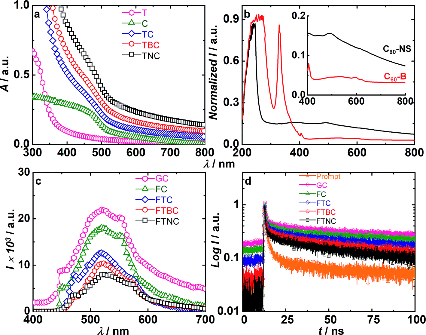 | ||
| Fig. 4 Absorbance spectra of (a) TiO2 (T), CdS (C), TiO2/CdS (TC), TiO2/C60-B/CdS (TBC) and TiO2/C60-NS/CdS (TNC) films and (b) C60-NS and C60-B; inset of (b) shows an enlarged view in the 400–800 nm range. (c) Fluorescence spectra and (d) emission decay of different photoanodes deposited on glass (G) and FTO (F) with λex = 370 nm and λem = 520 nm (in (d)). | ||
C60-NS can also therefore contribute as photosensitizers and improve the light harvesting capability of the QDSC. The TiO2/CdS film shows a broad absorption band in a visible region ranging from 400 to 550 nm. When C60-B deposited between TiO2 and CdS, there is an increase in the overall absorption intensity. Further, by incorporation of C60-NS between TiO2 and CdS, the absorbance is further increased compared to TiO2/C60-B/CdS, indicating that C60-NS are more effective than C60-B in capturing visible photons.
Fig. 4c shows the emission spectra of 5 films, i.e., glass/CdS, FTO/CdS, TiO2/CdS, TiO2/C60-B/CdS and TiO2/C60-NS/CdS films measured at an excitation wavelength of 370 nm. Glass/CdS reveals a broad emission peak at 520 nm caused by a radiative band edge recombination and emission from the transitions between the mid-gap states. Compared to this, the emission intensity of FTO/CdS film drops by 18% due to electron transfer from CdS to FTO. It drops by 42% for TiO2/CdS with respect to glass/CdS, due electron transfer from the conduction band (CB) of CdS to the CB of TiO2. Upon the inclusion of C60-B and C60-NS in the TiO2/CdS films, the emission intensity of CdS film is quenched by 52% and 64% respectively with respect to Glass/CdS. C60-NS is more efficient at accepting photo-excited electrons from the CB of CdS than C60-B.
To study the mechanism of excited electron deactivation from CdS, time-resolved emission decay plots were recorded and are shown in Fig. 4d. The decay data were fitted to a bi-exponential function for all the films.
I = B1![[thin space (1/6-em)]](https://www.rsc.org/images/entities/char_2009.gif) exp(−t/τ1) + B2exp(−t/τ2) exp(−t/τ1) + B2exp(−t/τ2)
| (2) |
Thus the electron life time was determined by the equation,
| 〈τ〉 = ΣBiτi2/ΣBiτi | (3) |
The average lifetime of glass/CdS film is 17 ns (Table S1†). τ1 corresponds to quenching via inter-particle charge transfer, and τ2 corresponds to the time for which the electron resides in the excited state prior to recombination with the holes in the valence band (VB) or trapping in the defect states. The τavg of the FTO/CdS and TiO2/CdS films are reduced to 12.98 and further to 6.76 ns. In the FTO/CdS film, τ1 is due to band edge recombination in CdS and τ2 is due to electron injection from CdS to FTO. In the TiO2/CdS film, τ1 is due to electron injection from CdS to TiO2 and τ2 is due to the band-gap electron–hole pairing. When C60-B and C60-NS are included between TiO2 and CdS, the depopulation pathway for electron transfer becomes facile, for they are well-established electron acceptors. The lowest lifetime achieved with C60-NS shows that a good contact exists between CdS and C60-NS and the NS are more conducive for accepting electrons from the CB of CdS than C60-B is. Therefore in TiO2/C60-B/CdS and TiO2/C60-NS/CdS, τ1 corresponds to electron transfer from CdS to TiO2/C60-NS or TiO2/C60-B, and τ2 corresponds to band-edge recombination. The rate constants for electron transfer from the CB of CdS to the CB of C60-B or C60-NS were calculated by using the following equations.
| ket = 1/〈τ〉 (TiO2/C60-B/CdS) − 1/〈τ〉 (TiO2/CdS) | (4) |
| ket = 1/〈τ〉 (TiO2/C60-NS/CdS) − 1/〈τ〉 (TiO2/CdS) | (5) |
Hence the rate constant for the electron transfer for C60-B and C60-NS are determined to be 0.575 × 10⁹ s−1 and 1.4 × 10⁹ s−1 respectively. This implied the faster electron transfer from the CB of CdS to C60-NS and this facilitated better charge extraction from C60-NS than from C60-B.
3.4 Counter electrode characterization
Raman spectra of C-cloth and MoS2/C-cloth are displayed in Fig. S2a.† The D- and G-bands are observed for both samples, which originates from carbon of the C-cloth. The D-band is due to defects owing to the presence of oxygen containing groups. The G-band is due to graphitic carbon, the sp2 hybridized carbon. The ID/IG ratio for C-cloth is 1.16 and for MoS2/C-cloth, it is 1.025 (Table S2, ESI†). Perhaps MoS2 passivates some of the surface defects on C-cloth. MoS2 also shows two peaks at 367 and 407 cm−1 corresponding to the E2g1 mode that arises from the in-plane vibration and the Ag1 from the out-of-plane vibrational mode of Mo–S bonds.38 Fig. S2b† shows the XRD pattern of MoS2 with peaks at 2θ = 14.1, 33.4 and 58.5° that correspond to d = 6.27, 2.68 and 1.58 Å which agree with the (002), (101), and (110) planes of a primitive lattice of a hexagonal structure (PDF: 371492). C-cloth shows a broad peaks at 2θ = 24.5 and 44.2° corresponding to d = 3.63 and 2.05 Å, matching with the (002) and (101) planes of graphitic carbon (PDF: 751621).Fig. 5a and b show the topography and surface potential maps of MoS2. Nano-sized particles of MoS2 are observed. They are discrete in some regions. The corresponding surface potential map shows the particles to be characterized by relatively higher potentials. The bright contrast corresponds to high potentials and the dark regions correspond to lower potentials. The work function of MoS2 is calculated using eqn (1). It was determined to be 4.6 eV by using a VCPD of 90 mV. This work function is suitable for electron transfer from C-cloth to MoS2, and then subsequently to the reduced electrolyte species during solar cell operation. Fig. 5c and d show the SEM images of C-cloth and MoS2/C-cloth. Pristine C-cloth displays a woven mat-like structure composed of intertwined fibers made up of carbon, which are smooth and continuous. MoS2/C-cloth shows MoS2 particles of no specific shape uniformly coated over the C-cloth, which is conducive for fast electron injection from C-cloth to MoS2, when its' used as a CE in a QDSC.
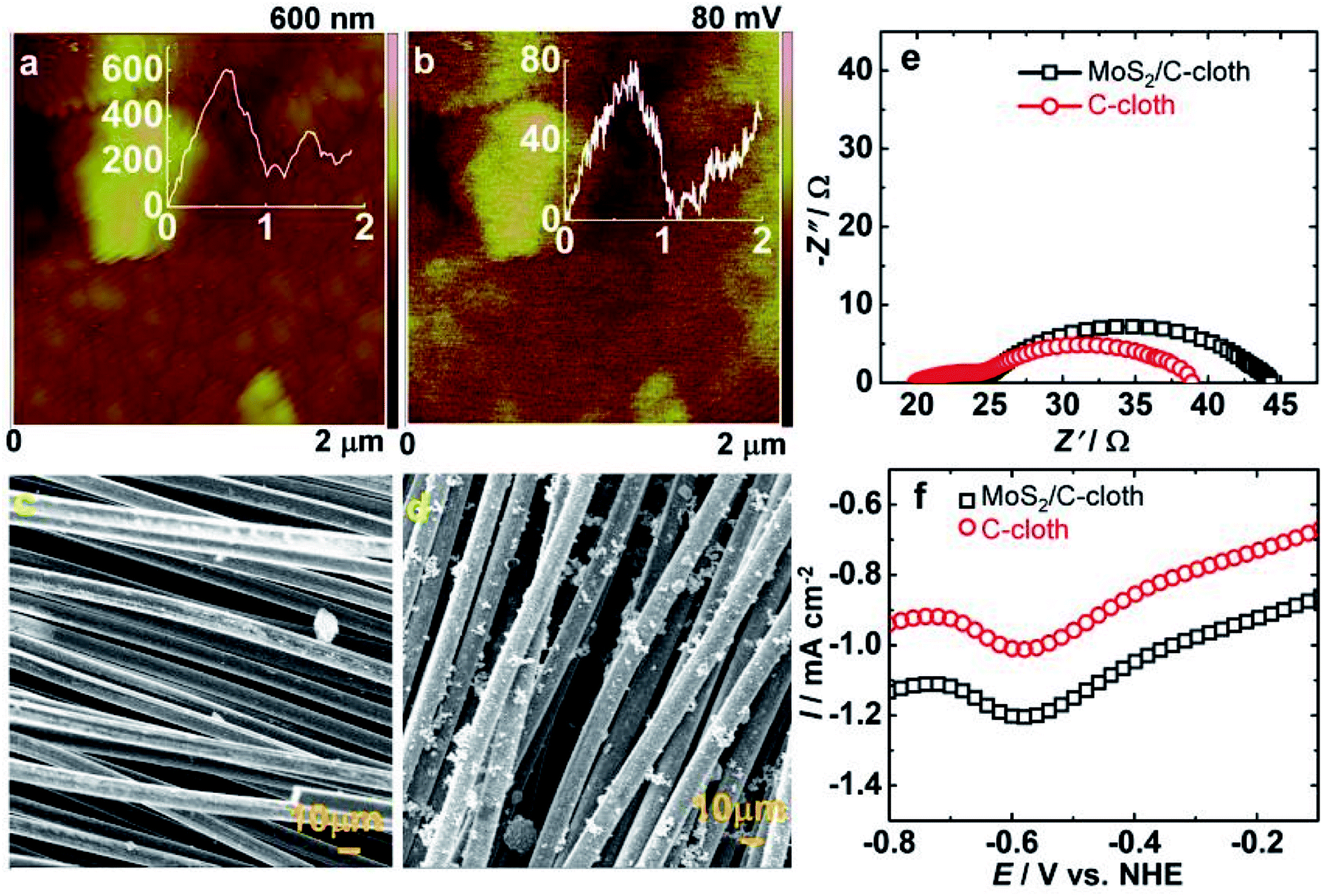 | ||
| Fig. 5 (a and b) Topography and surface potential images of MoS2 and (c and d) SEM images of C-cloth and MoS2/C-cloth, (e) Nyquist plots of CE cells in symmetric cell configurations and (f) linear sweep voltammograms of the two CEs (as working electrodes) in a 1 M Na2S, 1 M S solution in ultrapure water containing 0.2 M KCl as supporting electrolyte. A Pt rod was used as the auxiliary electrode, and an Ag/AgCl/KCl was used as a reference electrode. | ||
To further confirm the superior efficacy of the MoS2/C-cloth compared to C-cloth at transferring electrons to the electrolyte during cell operation, electrochemical impedance spectroscopy studies were performed. Symmetric cells of MoS2/C-cloth-polysulfide-MoS2/C-cloth and C-cloth-polysulfide-C-cloth configurations were constructed, and the corresponding Nyquist plots, recorded under a dc bias of 0 V, over a frequency range of 0.1 Hz to 1 MHz are compared in Fig. 5e. Here, RS, the high frequency real-axis intercept, represents the polysulfide and contact resistance, and RCT is a measure of the charge transfer resistance at the electrode/electrolyte interface and is equal to the diameter of the high to intermediate frequency skewed semicircle. The span of the second (low frequency) semicircle is a measure of the resistance to charge transfer at the grain boundaries (Rgb), which can be described as: C-cloth/MoS2 or MoS2/MoS2 or C-cloth/C-cloth boundaries, across the cross-section of the active material. Table S3 (ESI†) provides the impedance parameters. RCT and Rgb are lower and higher in magnitudes for the MoS2/C-cloth cell relative to the C-cloth cell suggestive of enhanced capability of MoS2/C-cloth to transfer electrons at the electrode/electrolyte interface, and also to propagate electrons across the active electrode, when used as a CE in a QDSC.
To compare the electrocatalytic activity of the two CEs for the reduction of the polysulfide species, linear sweep voltammetry was performed in a three electrode system containing C-cloth or MoS2/C-cloth as the working electrode, a Pt rod as the CE and Ag/AgCl/KCl as the reference electrode in a solution of 1 M S and 1 M Na2S with 0.2 M KCl as the supporting electrolyte (Fig. 5f). Both electrodes showed a reduction peak at −0.59 V, corresponding to the reduction of Sn2− to nS2−. MoS2/C-cloth exhibited a high current density for polysulfide reduction compared to C-cloth, which is indicative of a superior electrocatalytic activity in the former.
3.5 MoS2 as a supercapacitor electrode
In addition to the employing the MoS2/C-cloth electrode as a CE in QDSCs, the energy storage properties of this electrode were studied. To determine the supercapacitance performance of MoS2/C-cloth, cyclic voltammetry and galvanostatic charge–discharge measurements were recorded for symmetric cells based on the same and these are shown in Fig. 6. A sandwich type symmetric cell with two MoS2/C-cloth electrodes facing each other and separated by a separator soaked with 1 M KCl electrolyte was used. Cyclic voltammograms of the MoS2/C-cloth based symmetric cell were recorded at different scan rates of 5, 10, 30, 50, 80 and 100 mV s−1 in voltage ranges from −0.6 to 0.6 V and the comparative CV scans of C-cloth and MoS2/C-cloth at 100 mV s−1 scan rate are shown in Fig. 6a and b. The charge–discharge characteristics at different current densities of 2, 3, 5 and 10 A g−1 are shown in Fig. 6c. The cycling stability performance of the MoS2/C-cloth symmetric cell at 5 A g−1 was recorded over a similar voltage window (Fig. 6d). The specific capacitance (SC) in F g−1, energy density (E) in W h kg−1 and power density (P) in W kg−1 can be calculated from the following equations, obtained from the charge–discharge analysis shown in Table 1.| SC (F g−1) = I × Δt/ΔV | (6) |
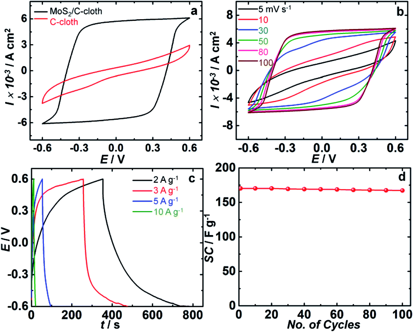 | ||
| Fig. 6 Cyclic voltammograms of MoS2/C-cloth and pristine C-cloth based symmetric cells recorded at 100 mV s−1 scan rate. (b) Cyclic voltammograms of MoS2/C-cloth symmetric cell at scan rates of 5, 10, 30, 50, 80, 100 mV s−1. (c) Galvanostatic charge–discharge characteristics of MoS2/C-cloth electrodes at different current densities (2, 3, 5, 10 A g−1). (d) Cycling stability performance of the MoS2/C-cloth based symmetric cell. | ||
| Current density, I (A g−1) | Discharge time, t (s) | Specific capacitance, SC (F g−1) | Energy density, E (W h kg−1) | Power density, P (kW kg−1) |
|---|---|---|---|---|
| 2 | 387 | 645 | 129 | 1.2 |
| 3 | 166 | 415 | 83 | 1.8 |
| 5 | 41 | 170.8 | 34.1 | 3 |
| 10 | 9.3 | 77.5 | 15.5 | 6 |
In (6), I is current density in A g−1, Δt is discharge time in s and ΔV is operating voltage window in V respectively.
| E (W h kg−1) = 0.5SC × ΔV2 × 1000/3600 | (7) |
| P (W kg−1) = 3600 × E/Δt | (8) |
The CV plot of C-cloth and MoS2/C-cloth are compared at a scan rate of 100 mV s−1 in the voltage window of −0.6 to 0.6 V. C-cloth shows a low enclosed area, an elliptical CV curve, while MoS2/C-cloth shows a rectangular CV curve with no redox peaks indicating a good electrochemical double layer capacitive behavior of MoS2. This implies a higher storage capacity for MoS2/C-cloth compared to sole C-cloth. Here C-cloth acts as a current collector, and the corresponding cell of C-cloth/KCl/C-cloth behaves largely like an electrolytic capacitor. The pseudocapacitive nature of MoS2 reaches a high performance by storing charge and releasing charge through oxidation and reduction. The in situ growth of MoS2 on C-cloth allows for a large the number of available electroactive sites.
The mechanism of the non-faradaic reaction is due to the formation of an electrical double layer of ions and electrons at the electrode/electrolyte interface by the adsorption of ions at the MoS2 surface.
| MoS2 + K+ + e− ↔ MoS2 − K+ | (9) |
Also, faradaic charge transfer occurs due to the diffusion of K+ into the interlayer of MoS2.
| MoS2 + K+ + e− ↔ MoS − SK+ | (10) |
Fig. 6b displays the CV curve of MoS2/C-cloth at various scan rates. It follows a rectangular type CV at higher scan rates and at lower scan rates it remained as elliptical. The anodic and cathodic current densities and the area under the curve increase as a function of scan rate. For instance, the anodic current density maxima increased from 4.2 to 6.1 mA cm−2 when the scan rate is raised from 5 to 100 mV s−1.
Galvanostatic charge–discharge of MoS2/C-cloth based symmetric cells at four different current densities (2, 3, 5, 10 A g−1) over a voltage window of −0.6 to 0.6 V are shown in Fig. 6c. It is observed that at a current density of 2 A g−1, the specific capacitance is found to be 645 F g−1 which is the highest capacitance value among four current densities. Moreover, with the increasing current densities, specific capacitance of MoS2/C-cloth decreased due to insufficient time for the ions to diffuse through the bulk of the 3D electrode. The energy density and power density at 2 A g−1 were calculated to be 129 W h kg−1 and 1.2 kW kg−1. At current densities of 3, 5 and 10 A g−1, the specific capacitances of the MoS2/C-cloth based cell were found to be 415, 170.8 and 77.5 F g −1 respectively. Fig. 6d shows the cycling stability of MoS2/C-cloth cell, and the capacitance decreased by 1.8% after 100 cycles.
3.6 Solar cell performances
QDSCs with the following photoanodes: TiO2/C60-NS/CdS, TiO2/C60-B/CdS and TiO2/CdS and the two CEs: MoS2/C-cloth and C-cloth are shown in Fig. 7a and b. With a given photoanode, the current density (J) versus voltage (V) response is collected from two cells. The J–V characteristics were obtained under 1 sun irradiance (AM 1.5 spectrum, 100 mW cm−2). Among all the cell, the TiO2/CdS cell shows the lowest PCE of about 3% and an open circuit voltage (VOC) of 661 mV with C-cloth as a CE. The TiO2/CdS anode, when coupled with a MoS2/C-cloth, yielded a PCE of 3.7% and a VOC of 685 mV. By the inclusion of C60-B between TiO2/CdS, the short circuit current density (JSC) increases from 11.3 to 14.2 mA cm−2. C60 alone may not be effective, but when used in combination with a photosensitizer, it transports electrons rapidly. With MoS2/C-cloth as the CE, the C60-B based cell shows a higher efficiency of about 4.9% and a higher VOC of 724 mV compared to the performance with pristine C-cloth as CE. In the latter, a PCE of 4.4% and a VOC of 650.8 mV is achieved. Higher VOC is attributed to the higher catalytic activity of MoS2, which drives the electrons to the polysulfide redox couple. The fill factor (FF) is high, and it is 0.47 with this CE. The highest PCE is 5.6%, achieved for the TiO2/C60-NS/CdS cell with a MoS2/C-cloth CE. By the inclusion of C60-NS in TiO2/CdS cell, a noticeable increment in JSC is observed, as it is now 16.2 mA cm−2. The higher JSC is indicative of the high electrical conductivity of C60-NS. For this cell, the VOC is 736.2 mV and FF is 0.47 greater than that obtained for an analogous cell having C-cloth as the CE, which delivers a PCE of 5.1%. The VOC and FF are 689.8 mV and 0.45% respectively. This difference clearly highlights the role of MoS2 in improving the electrocatalytic activity of C-cloth. The solar cell parameters are given in Table 2.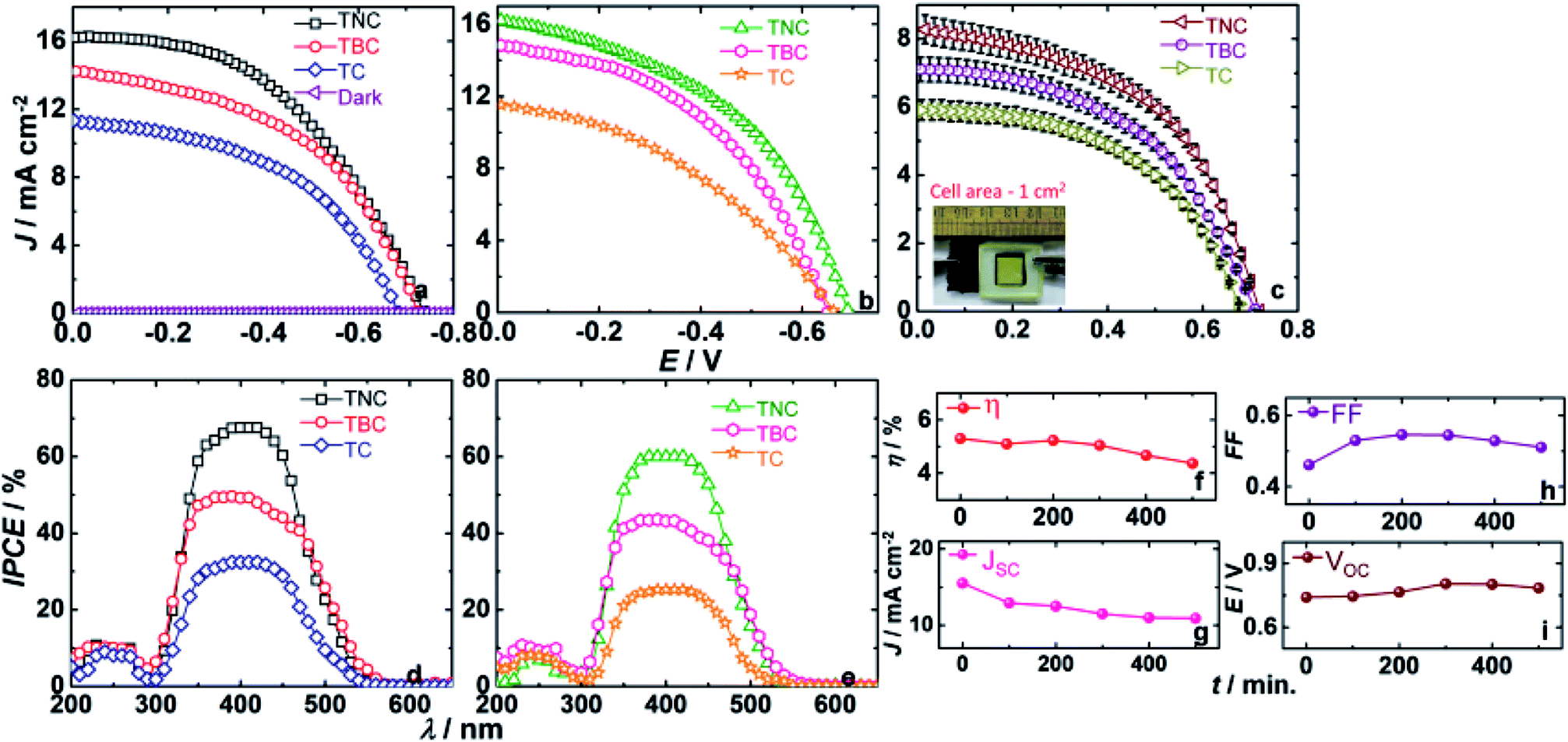 | ||
| Fig. 7 J–V characteristics of QDSCs with different photoanodes TiO2/CdS (TC), TiO2/C60-B/CdS (TBC) and TiO2/C60-N/CdS (TNC) under 1 sun illumination and in dark and with two CEs: (a) MoS2/C-cloth and (b) C-cloth, (c) J–V curves of QDSCs with large area photoanodes (area 1 cm2) under 1 sun illumination with MoS2/C-cloth CEs and a polysulfide gel electrolyte (inset is the photograph of the complete device in sandwich configuration) and IPCE versus wavelength of QDSCs with different photoanodes with two CEs: (d) MoS2/C-cloth and (e) C-cloth, temporal evolution of photovoltaic parameters (f) PCE; (g) JSC; (h) FF and (i) VOC, of a QDSC with a TiO2/C60-NS/CdS photoanode, and a MoS2/C-cloth as the CE. | ||
| Photoanode | C-cloth | MoS2/C-cloth | ||||||
|---|---|---|---|---|---|---|---|---|
| JSC (mA m−2) | VOC (mV) | FF | η (%) | JSC (mA cm−2) | VOC (mV) | FF | η (%) | |
| TiO2/CdS | ||||||||
| 1 | 11.5 | 661.0 | 0.39 | 3 | 11.3 | 685.0 | 0.48 | 3.7 |
| 2 | 10 | 694.7 | 0.43 | 3 | 10.8 | 721.6 | 0.46 | 3.6 |
|
||||||||
| TiO2/C60-B/CdS | ||||||||
| 1 | 14.8 | 650.8 | 0.45 | 4.4 | 14.2 | 724.0 | 0.47 | 4.9 |
| 2 | 13.5 | 700.4 | 0.45 | 4.2 | 13.3 | 724.0 | 0.50 | 4.8 |
|
||||||||
| TiO2/C60-NS/CdS | ||||||||
| 1 | 16.3 | 689.8 | 0.45 | 5.1 | 16.2 | 736.2 | 0.47 | 5.6 |
| 2 | 15.8 | 702.0 | 0.41 | 4.9 | 15.5 | 741.1 | 0.46 | 5.3 |
In addition to this, cells with photoanodes with large area (1 cm2) are assembled using MoS2/C-cloth CEs and a polysulfide gel electrolyte for J–V measurements shown in Fig. 7c. The lowest PCE of 2% is delivered by the TiO2/CdS film with a JSC of 5.9 mA cm−2 and VOC of 675 mV respectively. For the TiO2/C60-B/CdS cell, the photocurrent is enhanced to 7.2 mA cm−2 and VOC gradually increased to 692.3 mV exhibiting a high PCE of 2.5%. The fill factor is relatively higher than the previous cell. By the inclusion of C60-NS, charge transfer is easier than C60-B due to the high surface area and high conductivity of C60-NS. It helps in increasing photocurrent to 8 mA cm−2 with a VOC of 717.3 mV and FF of 51.5%. Hence, the highest PCE of 2.9% is obtained for the TiO2/C60-NS/CdS cell. The solar cell parameters are given in Table S4.†
IPCE versus wavelength plots of the cells with three photoanodes and with two different CEs are displayed in Fig. 7d and e. For a cell with a given photoanode, IPCEs of cells with MoS2/C-cloth CEs are higher than the IPCEs of cells with C-cloth as CEs. A TiO2/CdS cell exhibits a maximum IPCE of 32.4% at λ = 410 nm with MoS2/C-cloth as a CE. With C-cloth as a CE, the same shows a maximum IPCE of 25.3%. By the inclusion of C60-B, the IPCE of the cells with a TiO2/C60-B/CdS photoanode and MoS2/C-cloth and C-cloth CEs are increased to 48% and 43% respectively compared to TiO2/CdS based cells. The advantage of MoS2/C-cloth as CE is directly reflected in the IPCE values. When C60-NS is used in the TiO2/CdS photoanode, the maximum IPCE is 67.5%, which is the highest IPCE among all the photoanodes (with a MoS2/C-cloth CE). Compared to this, the TiO2/C60-NS/CdS cell with a C-cloth CE shows lower IPCE values of 60%. The superior ability of C60-NS to transport electrons is the reason for higher current efficiency among all cells.
Fig. 7f–i show the outcome of the stability test for the best cell assembly of TiO2/C60-NS/CdS photoanode and MoS2/C-cloth CE, and a polysulfide gel as the electrolyte. The cell is stored in open (under simulated sunlight). The J–V characteristics of the cell were measured at every 100 min interval and the solar cell parameters are given in Table S5.† Prior to each measurement, the polysulfide electrolyte was replenished. When the cell was measured for the first time, it shows a JSC of 15.5 mA cm−2. Gradually, the JSC decreases to 12.9 mA cm−2, after 100 min. In comparison, the VOC, initially and at 100 min, is almost the same. Surprisingly, on increasing exposure time, from 200 to 400 min, the VOC increases. This could be due to better penetration of the gel across the cross-section of the photoanode and the CE, with time. At 500 min, the decrease in VOC is minimal. FF also progressively increases with time, possibly due to the increase in photovoltage. PCE is nearly constant upto 200 min. It decreases by not a great degree, at 500 min, due to the decrease in JSC.
3.7 EIS studies on QDSCs
EIS studies were performed on QDSCs and the data was analysed with a standard model (Fig. 8).39–41 EIS spectra was recorded for the three photoanodes (TiO2/C60-NS/CdS, TiO2/C60-B/CdS and TiO2/CdS) using the same CE: MoS2/C-cloth using polysulfide gel electrolyte under dark conditions at different magnitudes of forward bias ranging from −0.3 to −0.75 V. Two skewed semicircles are observed in the Nyquist plots. The first semicircle in the high frequency region (first semicircle) is due to electron transport resistance through TiO2 and the second semicircle at intermediate frequency (second semicircle) region corresponds to charge transfer from photoanode to electrolyte. Nyquist plot was described through transmission line circuit. From Nyquist plots, EIS parameters such as chemical capacitance (Cμ), recombination resistance (Rrec), transport resistance (Rt) and dark current were determined, and plotted as a function of applied bias. Cμ is the electron density at Fermi level of TiO2. Rrec is the resistance offered to excited electron-oxidized polysulfide recombination at the photoanode/electrolyte interface. Rt is the resistance offered by the photoanode to electron injection to FTO. Fig. 8a shows the plot for chemical capacitance versus applied voltage. For all photoanodes, Cμ increases with increasing applied voltage. At −0.45 V and −0.75 V, Cμ for the C60-NS based cell are 10.5 and 42.5 mF cm−2. Cμ for TiO2/C60-NS/CdS cell is higher than that for the TiO2/C60-B/CdS and TiO2/CdS cell. Fig. 8b shows the variation of Rrec with applied voltage. Rrec is decreasing with increased applied bias and Rrec for TiO2/C60-NS/CdS cell was lower than the other two cells. The reason is unclear. Dark current decreases with increasing voltage (Fig. 8c). For C60-NS based cell, the dark current is the least. From Fig. 8d and e it is observed that as it is observed a gradual decreased impedance as the applied voltage increases.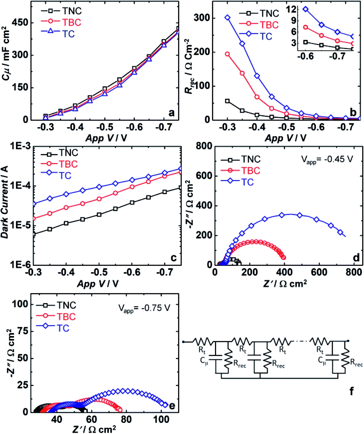 | ||
| Fig. 8 (a) EIS characterization of different photoanodes TiO2/CdS (TC), TiO2/C60-B/CdS (TBC) and TiO2/C60-NS/CdS (TNC): (a) Cμ, (b) Rrec, (c) dark current as a function of applied voltages, (d) and (e) Nyquist plots at −0.45 V and −0.75 V and (f) is a transmission line circuit. | ||
In the high frequency region, a 45° slant is observed at the commencement of the first semi-circle, which is representative of the electron diffusion through the TiO2 film. This line is one third of the transport resistance (Rt/3). Electrical conductivity can be determined from the transport resistance value i.e. σ = Rt/L, where L is the thickness of film. At −0.75 V, Rt of TiO2/CdS, TiO2/C60-B/CdS and TiO2/C60-NS/CdS based cells are 0.8, 0.74 and 0.54 Ω cm2 respectively (Table 3). In the C60-NS based cell, electron transport to FTO via TiO2 is more facile compared to the other two cells.
| Photoanode | −0.45 V | −0.75 V | ||||
|---|---|---|---|---|---|---|
| Rt (Ω cm2) | Rrec (Ω cm2) | Cμ (mF cm−2) | Rt (Ω cm2) | Rrec (Ω cm2) | Cμ (mF cm−2) | |
| TiO2/CdS | 1.6 | 688.6 | 8.7 | 0.8 | 48 | 40.6 |
| TiO2/C60-B/CdS | 1.5 | 341.8 | 9.4 | 0.74 | 28.9 | 41 |
| TiO2/C60-NS/CdS | 1 | 92.9 | 10.5 | 0.54 | 14 | 42.5 |
3.8 Performance of integrated device (QDSC and supercapacitor)
The TiO2/C60-NS/CdS–S2−/S–MoS2 based quantum dot solar cell is integrated with the MoS2//MoS2 symmetric supercapacitor supported over C-cloth current collectors, by electrically connecting the two cells. The solar cell comprises of TiO2/C60-NS/CdS as photoanode, MoS2/C-cloth as CE with a polysulfide gel electrolyte, whereas the supercapacitor contains two electrodes of MoS2/C-cloth separated by an aqueous KCl electrolyte in a symmetric configuration. The two cells are also connected to the potentiostat in a two electrode mode for measurements. A schematic and a photograph for the integrated device are shown in Fig. 9a and b. The solar cell of the integrated device is exposed to 1 sun illumination for 1 min and during this time, the voltage response of the supercapacitor is measured as function of time. The plot is shown in Fig. 9c.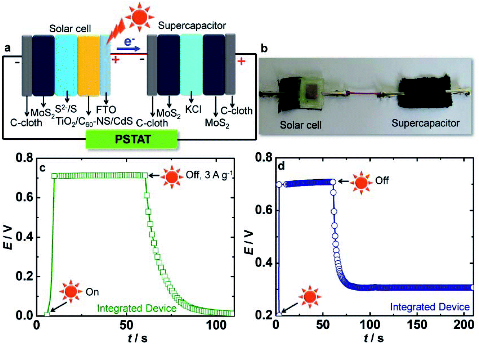 | ||
| Fig. 9 (a) Schematic and (b) photograph of the integrated device. (c) Photo-charging and discharge characteristics of an integrated device. Photo-charging is done under 1 sun illumination (100 mW cm−2) for 1 min followed by discharge under dark at 3 A g−1. (d) Self-discharge plot (under zero bias or current) obtained after photo-charging the integrated device. | ||
Upon illumination, the photocurrent produced by the solar cell is channeled to the MoS2 electrode of the supercapacitor. As anticipated, the MoS2 electrodes of the supercapacitor get photo-charged, as the voltage of the cell shows an abrupt increase from 0 to 0.7 V, and this voltage remains almost constant for the duration (of ∼1 min) for which the cell is illuminated. During this process, no current or voltage was applied to the supercapacitor or the solar cell from any external source, thus clearly illustrating that the supercapacitor is charged solely by the photocurrent generated by the solar cell, under irradiance. Upon switching off the light, and by applying an external current density of 3 A g−1 to the supercapacitor, the supercapacitor discharged to ∼0 V in 40 s. SC is found to be 171.4 F g−1 for the integrated device which is lower than the SC achieved for the sole supercapacitor. This could be due to the lower ΔV, and due to some (yet unclear) losses.
The energy density and the power density are 11.6 W h kg−1 and 1 kW kg−1 respectively. This performance reveals the capability of MoS2 to store the energy of solar cell in the supercapacitor. Fig. 9d shows the self-discharge process of the integrated device. Again, the device was charged to 0.7 V by exposure to 1 sun illumination for 1 min. After switching off the light, and by applying zero current or bias, the discharge process is monitored. The voltage readily reduced to a constant voltage of 0.25 V which is preserved retained for 200 s. This again shows that the device is capable of storing charge for reasonable durations.
4. Conclusions
A QDSC with a TiO2/C60-NS/CdS photoanode and a MoS2/C-cloth CE is fabricated and characterized. C60-NS have hexagonal-shapes and crystal structure, and they are more electrically conducting compared to bulk C60 (C60-B), perhaps due to their unique morphology. C60-NS have a deeper work function than C60-B with respect to vacuum level, and due to this suitably poised energy level and higher conductance, C60-NS also allow faster excited electron (from the CB of CdS) depopulation compared to C60-B, when used in a TiO2/CdS assembly. Besides the use of C60-NS in the photoanode for the first time, which leads to improved photovoltaic performance for the TiO2/C60-NS/CdS compared to the TiO2/C60-B/CdS and TiO2/CdS based cells, irrespective of the CE used, the potential of MoS2/C-cloth as a CE for QDSCs was also unravelled. MoS2 on C-cloth, resulted in improved electrocatalytic activity and lower charge transfer resistance for polysulfide reduction at the CE/electrolyte interface relative to pristine C-cloth. The higher electrical conductivity and a work function of 4.6 eV deduced for the MoS2/C-cloth electrode, also favors faster electron injection into the oxidized electrolyte during cell operation, compared to C-cloth. The champion cell with the TiO2/C60-NS/CdS photoanode and a MoS2/C-cloth CE, delivers a PCE of 5.6%, greater than that produced by the cells with TiO2/C60-B/CdS and TiO2/CdS photoanodes. With C-cloth as CE, the PCE of the TiO2/C60-NS/CdS photoanode based cell drops to 5.13%, illustrating the MoS2 effect. These studies show how promising C60-NS and MoS2 are in ameliorating the performance of QDSCs. The energy storage performance of the MoS2/C-cloth electrode was also evaluated by using it in a symmetric supercapacitor cell. The highest specific capacitance achieved by the MoS2/C-cloth cell is 645 F g−1 at 2 A g−1 current density, and the cell also showed rectangular cyclic voltammetric profile over a voltage window of 1.2 V. The MoS2/C-cloth electrode thus not only functions as an efficient CE for energy harvesting, but it is also a potential candidate for energy storage. By integrating the MoS2 supercapacitor with the QDSC, the resulting device was charged to 0.7 V, under 1 sun irradiance, without any other external bias or current.Conflicts of interest
There is no conflict of interest.Acknowledgements
Financial support from the Department of Science & Technology of India (Project: India-UK Center for education and research in clean energy (IUCERCE)), grant no (DST/RCUK/JVCCE/2015/04(1)(G)) is gratefully acknowledged.References
- S. Jiao, J. Du, Z. Du, D. Long, W. Jiang, Z. Pan, Y. Li and X. Zhong, J. Phys. Chem. Lett., 2017, 8, 559–564 CrossRef CAS PubMed.
- W. Wang, W. Feng, J. Du, W. Xue, L. Zhang, L. Zhao, Y. Li and X. Zhong, Adv. Mater., 2018, 30, 1705746 CrossRef PubMed.
- P. V. Kamat, J. Phys. Chem. C, 2008, 112, 18737–18753 CrossRef CAS.
- P. N. Kumar, S. Mandal, M. Deepa, A. K. Srivastava and A. G. Joshi, J. Phys. Chem. C, 2014, 118, 18924–18937 CrossRef CAS.
- R. Narayanan, M. Deepa and A. K. Srivastava, Phys. Chem. Chem. Phys., 2012, 14, 767–778 RSC.
- L. H. Lai, L. Protesescu, M. V Kovalenko and M. a. Loi, Phys. Chem. Chem. Phys., 2014, 16, 736–742 RSC.
- P. K. Santra, P. V. Nair, K. G. Thomas and P. V. Kamat, J. Phys. Chem. Lett., 2013, 4, 722–729 CrossRef CAS PubMed.
- K. Zhao, Z. Pan, I. Mora-Sero, E. Canovas, H. Wang, Y. Song, X. Gong, J. Wang, M. Bonn, J. Bisquert and X. Zhong, J. Am. Chem. Soc., 2015, 137, 5602–5609 CrossRef CAS PubMed.
- C. V. V. M. Gopi, M. V. Haritha, S. Kim and H. Kim, Nanoscale, 2015, 7, 12552–12563 RSC.
- Z. Ren, J. Wang, Z. Pan, K. Zhao, H. Zhang, Y. Li, Y. Zhao, I. Mora-Sero, J. Bisquert and X. Zhong, Chem. Mater., 2015, 27, 8398–8405 CrossRef CAS.
- J. Yang, J. Wang, K. Zhao, T. Izuishi, Y. Li, Q. Shen and X. Zhong, J. Phys. Chem. C, 2015, 119, 28800–28808 CrossRef CAS.
- W. Peng, J. Du, Z. Pan, N. Nakazawa, J. Sun, Z. Du, G. Shen, J. Yu, J. Hu, Q. Shen and X. Zhong, ACS Appl. Mater. Interfaces, 2017, 9, 5328–5336 CrossRef CAS PubMed.
- X. Miao, S. Tongay, M. K. Petterson, K. Berke, A. G. Rinzler, B. R. Appleton and A. F. Hebard, Nano Lett., 2012, 12, 2745–2750 CrossRef CAS PubMed.
- R. Narayanan, B. N. Reddy and M. Deepa, J. Phys. Chem. C, 2012, 116, 7189–7199 CrossRef CAS.
- S. Muduli, W. Lee, V. Dhas, S. Mujawar, M. Dubey, K. Vijayamohanan, S. H. Han and S. Ogale, ACS Appl. Mater. Interfaces, 2009, 1, 2030–2035 CrossRef CAS PubMed.
- P. V. Kamat, M. Haria and S. Hotchandani, J. Phys. Chem. B, 2004, 108, 5166–5170 CrossRef CAS.
- H. Xin, O. G. Reid, G. Ren, F. S. Kim, D. S. Ginger and S. A. Jenekhe, ACS Nano, 2010, 4, 1861–1872 CrossRef CAS PubMed.
- Y. Li, L. Zhao, Z. Du, J. Du, W. Wang, Y. Wang, L. Zhao, X. Cao and X. Zhong, J. Mater. Chem. A, 2018, 6, 2129–2138 RSC.
- L. Zhao, L. Zhao, W. Xue, W. fang, Y. Wang and Y. Li, Sol. Energy, 2018, 169, 505–511 CrossRef CAS.
- C. V. V. M. Gopi, M. V. Haritha, S. Kim and H. Kim, J. Power Sources, 2016, 311, 111–120 CrossRef CAS.
- C. V. V. M. Gopi, S. Singh, A. E. Reddy and H. Kim, ACS Appl. Mater. Interfaces, 2018, 10, 10036–10042 CrossRef CAS PubMed.
- C. V. V. M. Gopi, M. V. Haritha, Y. Lee and H. Kim, J. Mater. Chem. A, 2016, 4, 8161–8171 RSC.
- C. V. V. M. Gopi, S. Ravi, S. S. Rao, A. E. Reddy and H. Kim, Sci. Rep., 2017, 7, 46519 CrossRef PubMed.
- C. V. V. M. Gopi, A. E. Reddy and H. Kim, J. Mater. Chem. A, 2018, 6, 7439–7448 RSC.
- J. Xie, J. Zhang, S. Li, F. Grote, X. Zhang, H. Zhang, R. Wang, Y. Lie, B. Pan and Y. Xie, J. Am. Chem. Soc., 2017, 135, 17881–17888 CrossRef PubMed.
- D. Barpuzary, A. Banik, G. Gogoia and M. Qureshi, J. Mater. Chem. A, 2015, 3, 14378–14388 RSC.
- B. Lei, G. R. Li and X. P. Gao, J. Mater. Chem. A, 2014, 2, 3919–3925 RSC.
- S.-Y. Tai, C.-J. Liu, S.-W. Chou, F. S.-S. Chien, J.-Y. Lin and T.-W. Lin, J. Mater. Chem., 2012, 22, 24753–24759 RSC.
- M. Seol, D. H. Youn, J. Y. Kim, J.-W. Jang, M. Choi, J. S. Lee and K. Yong, Adv. Energy Mater., 2014, 4, 1300775 CrossRef.
- G. Ma, H. Peng, J. Mu, H. Huang, X. Zhou and Z. Lei, J. Power Sources, 2013, 229, 72–78 CrossRef CAS.
- K.-J. Huang, L. Wang, Y. J. Liu, H. B. Wang, Y. M. Liu and L.-L. Wang, Electrochim. Acta, 2013, 109, 587–594 CrossRef CAS.
- K.-J. Huang, L. Wang, Y.-J. Liu, Y.-M. Liu, H.-B. Wang, T. Gan and L.-L. Wang, Int. J. Hydrogen Energy, 2013, 38, 14027–14034 CrossRef CAS.
- M. Sathish and K. Miyazawa, J. Am. Chem. Soc., 2007, 129, 13816–13817 CrossRef CAS PubMed.
- H. Yu, X. Yu, Y. Chen, S. Zhang, P. Gao and C. Li, Nanoscale, 2015, 7, 8731–8738 RSC.
- M. Sathish and K. Miyazawa, Molecules, 2012, 17, 3858–3865 CrossRef CAS PubMed.
- M. C. Martin, D. Koller, A. Rosenberg, C. Kendziora and L. Mihaly, Phys. Rev. B, 1995, 51, 3210–3213 CrossRef CAS.
- S. Leach, M. Vervloet, A. Despres, E. Breheret, J. P. Hare, T. J. Dennis, H. W. Kroto, R. Taylor and D. R. M. Walton, Chem. Phys., 1992, 160, 451–466 CrossRef CAS.
- R. N. Bulakhe, V. N. Nguyen and J. J. Shim, New J. Chem., 2017, 41, 1473–1482 RSC.
- V. Gonzalez-Pedro, X. Xu, I. Mora-Sero and J. Bisquert, ACS Nano, 2010, 4, 5783–5790 CrossRef CAS PubMed.
- J. Wang, I. Mora-Sero, Z. Pan, K. Zhao, H. Zhang, Y. Feng, G. Wang, X. Zhong and J. Bisquert, J. Am. Chem. Soc., 2013, 135, 15913–15922 CrossRef CAS PubMed.
- I. Mora-Sero, S. Gimenez, F. Fabregat-Santiago, R. Gomez, Q. Shen, T. Toyoda and J. Bisquert, Acc. Chem. Res., 2009, 42, 1848–1857 CrossRef CAS PubMed.
Footnote |
| † Electronic supplementary information (ESI) available: Cyclic voltammetry of pristine TiO2 and CdS, XRD and Raman spectra of MoS2, C-cloth and MoS2/C-cloth, tables of emission decay fitting parameters of photoactive films, Raman and EIS data of counter electrodes, solar cell parameters of large area (1 cm2) QDSCs using MoS2/C-cloth CE and stability performance of QDSCs at 100 min interval of time. See DOI: 10.1039/c8ra04956d |
| This journal is © The Royal Society of Chemistry 2018 |