
 Open Access Article
 This Open Access Article is licensed under a
 Creative Commons Attribution 3.0 Unported Licence
Annealing temperature effects on photoelectrochemical performance of bismuth vanadate thin film photoelectrodes†
Le Shi a,
Sifei Zhuoa,
Mutalifu Abulikemua,
Gangaiah Mettelaa,
Thangavelu Palaniselvama,
Shahid Rasula,
Bo Tanga,
Buyi Yanb,
Navid B. Salehc and
Peng Wang*a
a,
Sifei Zhuoa,
Mutalifu Abulikemua,
Gangaiah Mettelaa,
Thangavelu Palaniselvama,
Shahid Rasula,
Bo Tanga,
Buyi Yanb,
Navid B. Salehc and
Peng Wang*a
aWater Desalination and Reuse Center, Division of Biological and Environmental Sciences and Engineering, King Abdullah University of Science and Technology, Thuwal 23955-6900, Saudi Arabia. E-mail: peng.wang@kaust.edu.sa
bDivision of Physical Science and Engineering, King Abdullah University of Science and Technology, Thuwal 23955-6900, Saudi Arabia
cDepartment of Civil, Architectural and Environmental Engineering, University of Texas at Austin, Austin, TX 78712, USA
First published on 16th August 2018
Abstract
The effects of annealing treatment between 400 °C and 540 °C on crystallization behavior, grain size, electrochemical (EC) and photoelectrochemical (PEC) oxygen evolution reaction (OER) performances of bismuth vanadate (BiVO4) thin films are investigated in this work. The results show that higher temperature leads to larger grain size, improved crystallinity, and better crystal orientation for the BiVO4 thin film electrodes. Under air-mass 1.5 global (AM 1.5) solar light illumination, the BiVO4 thin film prepared at a higher annealing temperature (500–540 °C) shows better PEC OER performance. Also, the OER photocurrent density increased from 0.25 mA cm−2 to 1.27 mA cm−2 and that of the oxidation of sulfite, a hole scavenger, increased from 1.39 to 2.53 mA cm−2 for the samples prepared from 400 °C to 540 °C. Open-circuit photovoltage decay (OCPVD) measurement indicates that BiVO4 samples prepared at the higher annealing temperature have less charge recombination and longer electron lifetime. However, the BiVO4 samples prepared at lower annealing temperature have better EC performance in the absence of light illumination and more electrochemically active surface sites, which are negatively related to electrochemical double-layer capacitance (Cdl). Cdl was 0.0074 mF cm−2 at 400 °C and it decreased to 0.0006 mF cm−2 at 540 °C. The OER and sulfide oxidation are carefully compared and these show that the efficiency of charge transport in the bulk (ηbulk) and on the surface (ηsurface) of the BiVO4 thin film electrode are improved with the increase in the annealing temperature. The mechanism behind the light-condition-dependent role of the annealing treatment is also discussed.
1. Introduction
Harvesting solar energy is an effective alternative energy pathway and is desired to mitigate environmental impacts from fossil fuel based energy production.1,2 Photoelectrochemical (PEC) water splitting with metal oxide semiconductors has attracted enormous attention in solar energy conversion.3–5 Recently, bismuth vanadate (BiVO4), an n-type bimetallic oxide semiconductor with a narrow band gap (∼2.4 eV), suitable band position, and relatively high stability against photo-corrosion, has distinguished itself as a promising photoanode-material.6,7 However, pristine BiVO4 has poor electron–hole separation8 and exhibits slow water oxidation kinetics,9 which are major obstacles to utilization of the photoreactive capacity of this material.Recent research has invested into multiple strategies in improving the PEC performance of BiVO4, including heterojunction formation, (e.g., Co3O4/BiVO4,10 SnO2/BiVO4,11 WO3/BiVO4,12 TiO2/BiVO4,13,14 AgFeS2–BiVO4 (ref. 15)), doping with Mo or W,16–18 addition of electron collectors,19 Plasmonic enhancement,20–23 and addition of co-catalysts, such as Co–Pi,9,24 α-Fe2O3,25 NiCoO2,26 and Ir–COOH.27 A closer investigation reveals that there exists a large variation in the generated current (Table S1†). Literature reports also highlight the lack of consistency in sample preparation process, including the precursor composition, annealing temperature, etc. (Table S1†). Different materials need different optimal annealing temperature and different synthesis conditions. In fact, the annealing temperature is recognized as an essential and critical step in crystallization of BiVO4,28–31 but how annealing temperature affects the PEC performance, specially that of BiVO4 thin film electrode, is largely unexplored.
In this study, we systematically investigate the effects of annealing temperature (400–540 °C) on crystallization behavior, surface morphology, and grain size of BiVO4 thin film photoelectrodes, prepared by spin-coating. The electrochemical (EC) and PEC performances of the BiVO4 thin film photoelectrodes are carefully assessed in relation to the annealing temperature and other parameters affected by the annealing temperature. First, under dark condition, BiVO4 thin film electrodes prepared at lower temperature produce better electrochemical performance, which might be due to the more electrochemically active sites. Second, under AM 1.5 irradiated conditions, BiVO4 thin film electrodes prepared at higher annealing temperature produce higher photocurrent density. The OER photocurrent density was increased from 0.25 mA cm−2 to 1.27 mA cm−2 for the samples prepared from 400 °C to 540 °C, which might be due to the less charge recombination controlled by higher degree of crystallinity and bigger grain size, and also better crystal orientation for O2 evolution. This work will attract attention on the annealing temperature effect on the EC and PEC performance of BiVO4 based thin film electrode.
2. Experimental
2.1 Reagents and materials
Bismuth(III) nitrate pentahydrate (Bi(NO3)3·5H2O, purity ≥ 98%), vanadyl acetylacetonate (VO(acac)2, purity ≥ 98%), acetylacetone (purity ≥ 99%), and methylene blue were procured from Sigma Aldrich (St. Louis, MO, USA). The conductive fluorine-doped tin oxide (FTO) coated glass with a sheet resistance of 7 Ω sq−1 was purchased from Xinyan (Xinyan Technology Co., China). All aqueous solutions were prepared with Millipore deionized (DI) water with a resistivity of 18.2 MΩ cm.2.2 Preparation of BiVO4 thin film photoelectrodes
The BiVO4 thin films were prepared by spin-coating and in a layer-by-layer fashion. First, the precursor solution was prepared by dissolving 0.40 g of Bi(NO3)3·5H2O and 0.22 g of VO(acac)2 in 10 mL acetylacetone, under sonication for 10 h with gentle heating at 40 °C; a dark brown and transparent solution of 80 mM of bismuth and 80 mM of vanadium (atomic ratio Bi/V = 1) in acetylacetone was finally obtained.The fluorine-doped tin oxide glass (FTO glass) was pre-cleaned following a multi-step procedure described as follows: sonication for 20 min in DI water containing 3 wt% sodium dodecyl sulfate (SDS), sonication for another 20 min in DI water, followed by sonication for 20 min in acetone, and finally sonication for 20 min in ethanol (96%) prior to storing in ethanol. The pre-cleaned FTO glass was dried under nitrogen, followed by cleaning with a Plasma cleaner (Harrick Plasma, Ithaca NY, USA) for 2 min, immediately prior to using it as a substrate in spin-coating of the BiVO4 thin film.
The precursor solution of 80 μL was spin-coated at 1400 rpm for 20 s on a CHEMAT Technology Spin coater (KW-4A, Northridge, CA) onto a 2.5 × 2.5 cm FTO substrate to ensure complete coverage. Upon evaporation of excess solvent on a hotplate at 100 °C for 2 min in ambient air, the coated FTO was heated up to 400–540 °C for 5 min in air for pre-crystallization. Four pre-crystallization temperatures, i.e., 400, 450, 500 and 540 °C, were investigated in this step. The samples were then cooled for 5 min in ambient condition. Multiple samples with 2, 4, 6, and 8 layers of coatings, were prepared for comparison. After deposition of the final layer, the BiVO4 coated FTO electrode was heated on a hotplate at 100 °C for 2 min, followed by annealing in a muffle furnace at the pre-crystallization temperature for 0.6 h and at a heating rate of 2 °C min−1 for further crystallization. The samples were labeled as BiVO4-n, with n being the pre-crystallization and annealing temperature.
2.3 Material characterization
The surface characteristics of the BiVO4-n electrodes were investigated by field-emission scanning electron microscopy (FESEM, Zeiss Merlin, Germany). Surface roughness analysis was carried out by atomic force microscopy (AFM, Agilent 5400SPM, Agilent Technologies, USA), at scan areas of 2.0 × 2.0 μm and 5.0 × 5.0 μm for all samples. Powdered X-ray diffraction (XRD, Bruker D8 Advance diffractometer, USA, using Cu Kα radiation, λ = 1.5418 Å) was used to characterize the crystallinity of the samples. All samples were analyzed by XRD in the range of 15–70° at a scan rate of 0.5° min−1; the crystal sizes of the BiVO4-n were estimated with the Scherrer formula.32 The diffuse reflectance UV-Vis absorption spectra of the samples were recorded with a spectrophotometer (UV 2550, Shimadzu, Japan), with fine BaSO4 powder as a reference. In thermal gravimetric analysis (TGA, NETZSCH, Germany),100 μL precursor was vacuum-dried for 5 h prior to the measurements. X-ray photoelectron spectroscopy (XPS) results were collected by an Axis Ultra instrument (Kratos Analytical) under ultrahigh vacuum (<10−8 torr) and by using a monochromatic Al Kα X-ray source. The adventitious carbon 1s peak was calibrated at 285 eV and used as an internal standard to compensate for any charging effects.2.4 PEC performance assessment
The PEC performances of the prepared BiVO4-n photoelectrodes were evaluated by using a three-electrode configuration (Autolab, PGSTAT302N, Metrohm, The Netherlands), where BiVO4-n electrode was the working electrode, Pt mesh was the counter electrode, and Ag/AgCl in 3 M KCl was the reference electrode. All the three electrodes were immersed in a 60 mL quartz container containing a supporting electrolyte. The supporting electrolyte used in all the PEC systems was 0.1 M phosphate (KPi) buffer solution (pH 7), unless otherwise specified. Prior to PEC measurement, the electrolyte was purged with N2 for 30 min to remove dissolved O2 from the electrolyte solution. Light was irradiated from a solar simulator (Oriel® Sol1A Class ABB Solar simulators, Newport, USA). The intensity of the light source was calibrated with a Si diode (Model 818, Newport, USA) to simulate air-mass 1.5 global (AM 1.5) solar light illumination (100 mW cm−2). Electrochemical impedance spectroscopy (EIS) was carried out by applying an AC voltage amplitude of 10 mV within the frequency range from 105 to 10−3 in 0.1 M KPi buffer solution under both dark condition and AM 1.5 illumination. The open-circuit photovoltage decay (OCPVD) was monitored by measuring the photovoltage of samples at open circuit condition under irradiated condition followed by dark condition (to observe decay curves). The incident-photon to current efficiency (IPCE) spectra was acquired under irradiated condition. The light from a 300 W Xe lamp (Model 73404, Newport, USA) was focused through the monochromator (Model: 74125, Newport, USA) onto the working electrode, and the monochromator was incremented in the spectral range (350–600 nm) with a sampling interval of 10 nm and a current sampling time of 50 s. The light intensity and the generated photocurrent were measured with Newport power meter (Model 1918-R, Newport, USA) and Autolab electrochemical workstation (Autolab, PGSTAT302N, Metrohm, The Netherlands), respectively.3. Results and discussions
3.1 Preparation of the photoelectrodes
The BiVO4 thin film photoelectrodes are prepared by the layer-by-layer spin-coating method. The detailed sample synthesis is described in the Experimental part. It is noteworthy that a gentle heating is necessary for preparing the precursor solution to make sure its coloration changes from green to dark brown before applying it to spin-coating (Fig. S1†).33,34 The spin-coating cycles of 2, 4, 6, and 8 are tested and compared in this study. The UV-Vis spectra of the BiVO4 samples indicate that the light absorption by the samples increases with the number of layers and begins to plateau at and beyond 6 layers (Fig. S2†). Thus, the BiVO4 samples with 6 layers are utilized hereinafter, unless otherwise specified. Using the cross-section SEM image (Fig. S3†), the thickness of the 6-layers BiVO4 thin film is estimated to be ∼93 nm, which is near the estimated optimal hole diffusion length in BiVO4 (∼100 nm).34There are two heating steps in the sample preparation: brief and multiple heating in ambient air for pre-crystallization upon coating each layer and annealing in a muffle furnace at the end after the completion of coating all layers. To assess the effect of temperature on grain size of BiVO4, 400, 450, 500 and 540 °C conditions are investigated in both pre-crystallization and annealing steps. For the purpose of simplification, the temperatures of the pre-crystallization and annealing for the same sample are kept the same in this study. The temperature range is chosen based on the thermal gravimetric analysis (TGA) (Fig. S4†). The TGA result shows a clear weight change of the BiVO4 before 400 °C, indicating the conversion of the precursor to BiVO4 has to be accomplished above 400 °C, and this is in agreement with the literature report.35 Considering the fact that the FTO glass (7 Ω sq−1, Xinyan, Inc.) is produced with the annealing temperature of 600 °C, 540 °C is chosen to be the highest annealing temperature in this work. XRD results of BVO-540 samples annealed at different duration time are presented Fig. S5,† which indicate that 0.6 h annealing duration is long enough for complete crystallization.
3.2 Crystallinity and light absorption properties of the photoelectrodes
The diffraction peaks at 18.9°, 28.9°, 30.56°, 40.05° and 42.5° (Fig. 1a) of the XRD spectrum identify that all BiVO4 samples possess a scheelite-monoclinic (s-m) phase (JCPDS 14-0688), which is known for its improved photocatalytic activity in O2 evolution among all the BiVO4 crystalline phases;28,37,38 scheelite-tetragonal (s-t) and zircon-tetragonal (z-t) are the other two crystal phases. It should be noted that no bismuth or vanadium oxide phase impurities have been identified. The additional diffraction peaks observed can be assigned to the FTO substrate, as expected from a thin BiVO4 coated glass surface.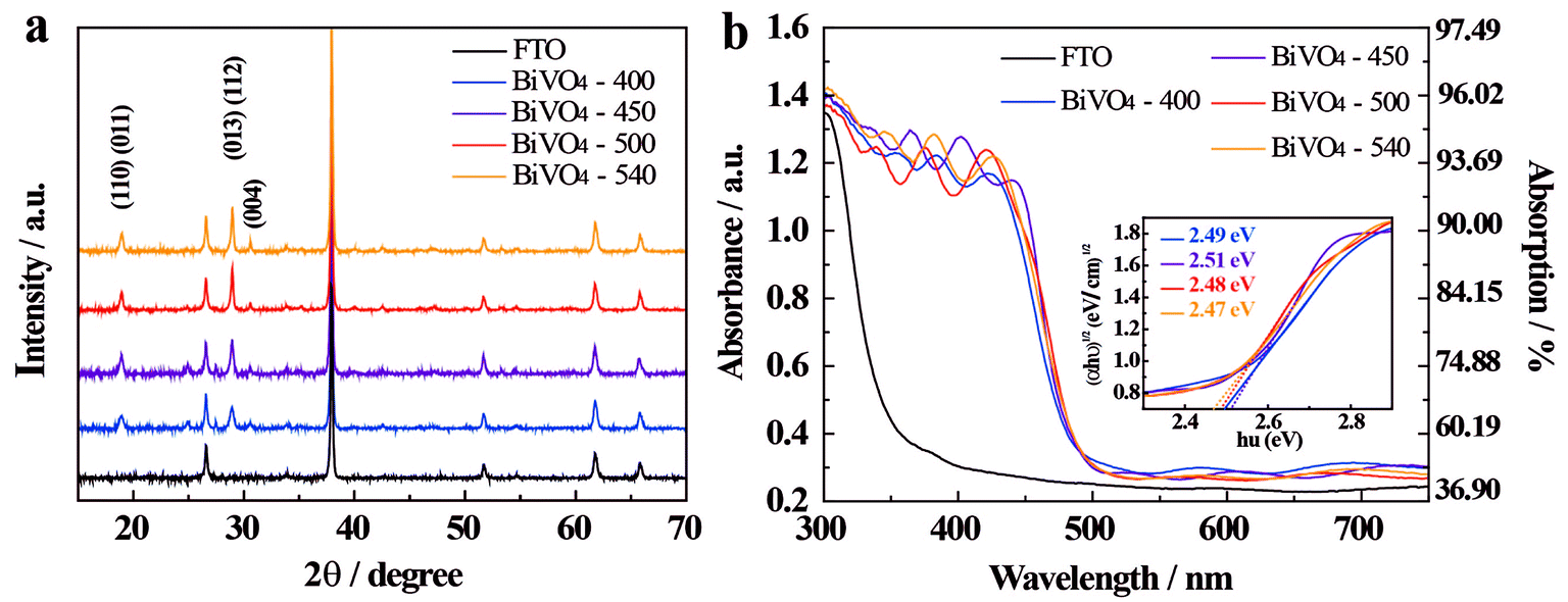 | ||
| Fig. 1 (a) XRD spectra and (b) UV-Vis absorption spectra of BiVO4-n samples; FTO-glass control spectrum is also presented. Absorption Y and absorbance log10(1/(1 − Y)) were measured between 300 and 750 nm. Inset in (b) shows transformed Kubelka–Munk functions36 for each sample as a function of energy of illumination. | ||
The full width at half maximum (FWHM) at the peak (013) (112) is 0.408, 0.312, 0.229, and 0.114 for BiVO4-400, BiVO4-450, BiVO4-500, and BiVO4-540, respectively, and this decreasing trend with the increase in annealing temperature indicates that the crystallinity of BiVO4 improves with annealing temperature. The crystal sizes are calculated using the Scherrer formula:
 | (1) |
Moreover, the peak intensity ratios of the (004) and (112) facets are 0.213, 0.172, 0.178, and 0.227 for BiVO4-400, BiVO4-450, BiVO4-500, and BiVO4-540, respectively; while those of the (004) and (110) facets are 0.357, 0.313, 0.400, and 0.550 for BiVO4-400, BiVO4-450, BiVO4-500, and BiVO4-540, respectively. It is evident that when the annealing temperature is higher than 450 °C, the fraction of exposed (004) surface in BiVO4 thin film electrode increases significantly. This enhancement in the exposure of (004) crystal facets is known to be beneficial for PEC water oxidation as these facets may provide active sites for O2 evolution.39–41 These results demonstrate that the annealing temperature significantly affects the crystallinity and crystal orientation of the BiVO4 thin-film. In addition, the diffraction peat at 25° is coming from adsorbed carbon contaminants in the sample preparation process, which can be completely removed by increasing the annealing temperature. XPS analysis was carried out to gain addition insights (Fig. S6†) and all the discussion in details are presented in ESI.†
The effect of the annealing temperature on the light absorption properties is investigated by UV-Vis absorption and diffuse reflectance spectra7,42,43 (Fig. 1b and S7†) and the results show no obvious effect in the temperature range tested. This is likely due to the similar thickness of the samples as these are coated with the same number of layers. Interestingly, both periodic absorption and reflection peaks are observed, which are likely a result of a periodically ordered surface morphology and of uniform size of the grains in the BiVO4 thin films.44
3.3 Surface morphology of the photoelectrodes
Fig. 2 presents representative SEM images of the BiVO4-n samples; the crystals appear to be sintered together to form a relatively compact thin film. However, some surface cavities are visible in BiVO4-400, and these cavities begin to disappear with the increase in annealing temperature. The surface grain sizes are observed to be smaller in BiVO4-400 and BiVO4-450, compared to those in BiVO4-500 and BiVO4-540 samples, which further illustrate the effect of annealing temperature on grain size. The grain size distributions are derived from the SEM images in Fig. 2. Average grain size and grain size range increase with annealing temperature (Table S2†). These results suggest that the higher temperature favors crystals with larger grain size. The estimated coefficients of variation of the grain size indicate that grain size distribution is not uniform at 540 °C (Table S2†). Furthermore, the average grain sizes estimated from SEM images (Fig. 2) show similar trend when compared to the crystal sizes estimated from XRD analyses (Table S3†). These results imply that the BiVO4 grains are largely single crystal in each grain in the thin film photoelectrodes prepared especially at lower temperature.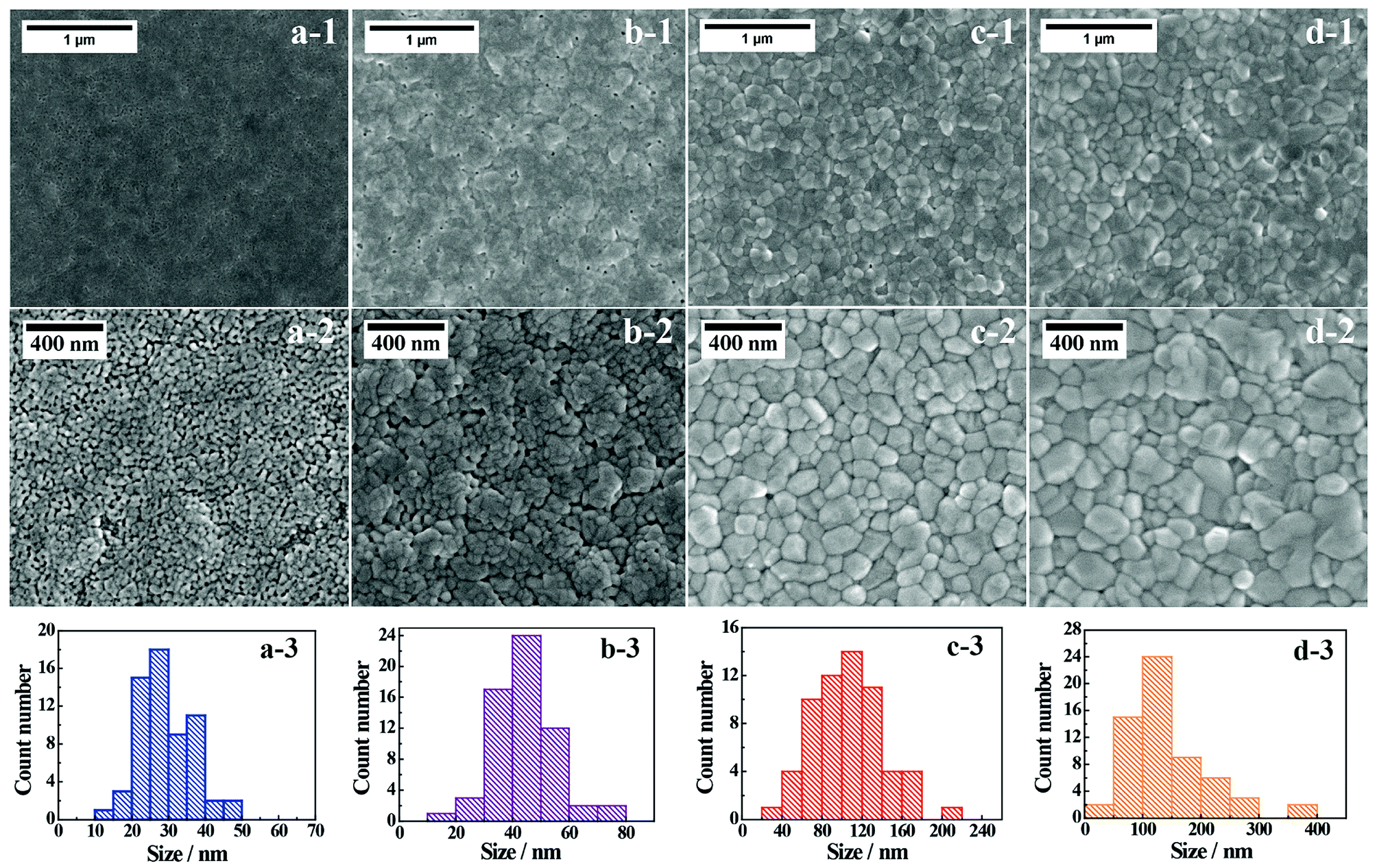 | ||
| Fig. 2 Top view SEM images of (a1 and a2) BiVO4-400, (b1 and b2) BiVO4-450, (c1 and c2) BiVO4-500, and (d1 and d2) BiVO4-540. Grain size (nm) distributions derived from SEM images of each sample (a3–d3). | ||
AFM analysis is conducted to investigate surface morphology of the thin film BiVO4 photoelectrodes (Fig. S8 and S9†). Root-mean-square roughness (Rms), a reliable parameter for quantifying surface micro-roughness,45 is estimated as 12.9 nm, 13.8 nm, 13.7 nm, and 13.5 nm for BiVO4-400, BiVO4-450, BiVO4-500, and BiVO4-540, respectively. The annealing temperature shows little effect on surface roughness changes among the BiVO4-n photoelectrodes.
3.4 PEC performances of the photoelectrodes
The PEC performances of BiVO4-n samples are investigated in a standard three-electrode system and under illumination with a standard AM 1.5G simulated solar light (100 mW cm−2). The irradiated was incident on the backside of the BiVO4 photoelectrodes, i.e., on the side with no exposed BiVO4 thin film. The potential is reported against the reversible hydrogen electrode (RHE) with the following equation:
 | (2) |
 is the potential of the silver chloride electrode with respect to normal hydrogen electrode (NHE), which is 0.1976 V at 25 °C.
The linear sweep voltammetry (LSV) curves presented in Fig. 3a show that the photocurrents increase with increasing potential, which is expected when enhanced band bending occurs, and when electron–hole recombination (at high potential) is reduced.46 The photocurrents at 1.23 V vs. RHE in 0.1 M KPi solution increase with increasing annealing temperature (0.25, 0.69, 1.18, and 1.27 mA cm−2 for BiVO4-400, BiVO4-450, BiVO4-500 and BiVO4-540, respectively) (Fig. 3a).
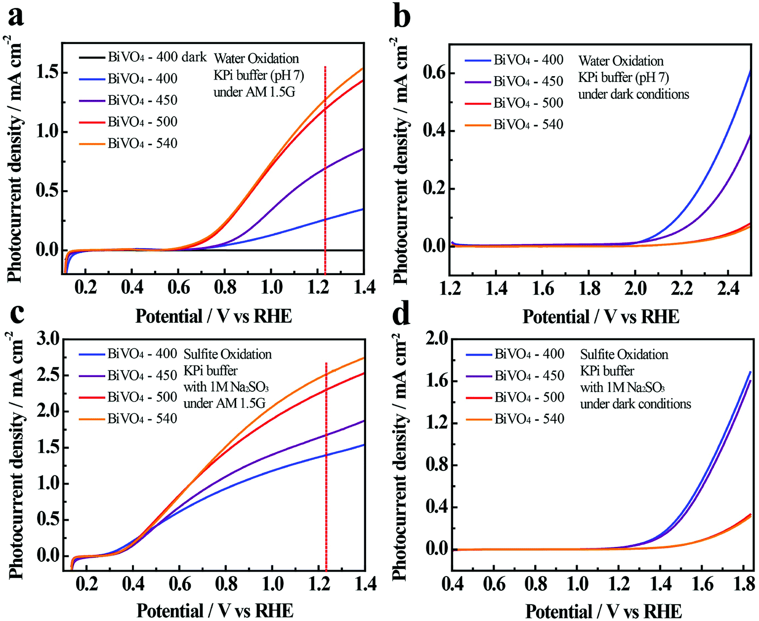 | ||
| Fig. 3 Linear sweep voltammetry (LSV) curves of BiVO4-n samples obtained at a scan rate of 5 mV s−1 in dark or under AM 1.5 illumination. Water oxidation in 0.1 M potassium phosphate (KPi) buffer (pH-7) under illuminated (a) and dark (b) conditions. Sulfite oxidation in 0.1 M KPi, containing 1 M Na2SO3 under illuminated (c) and dark (d) conditions. | ||
To investigate the surface reaction kinetics of BiVO4-n samples, the PEC performances of the BiVO4 photoelectrodes are also measured in the presence of a hole-scavenger in the electrolyte (i.e., in this case, 1 M Na2SO3 in 0.1 M KPi) (Fig. 3c and d). Results indicate that PEC performance is enhanced with sulfite oxidation (Fig. 3c) compared to water oxidation (Fig. 3a). The photocurrent densities are 1.39, 1.68, 2.31, and 2.53 mA cm−2 for BiVO4-400, BiVO4-450, BiVO4-500 and BiVO4-540, respectively at 1.23 V vs. RHE.
The comparison provides convincing evidence of poor water oxidation kinetics by the BiVO4 thin film photoelectrodes, which is likely caused by the competition between the surface charge transfer and charge recombination.47
The poor water oxidation kinetics of BiVO4-n samples is also evidenced in the large photocurrent transients, when illumination is turned on and off (Fig. S10†). The photoresponse of the samples over time is measured at 1.23 V vs. RHE in 0.1 M KPi buffer (Fig. S10a†) and in 0.1 M KPi containing 1 M Na2SO3 (Fig. S10b†) under AM 1.5G illumination with 50 s light on/off cycles. Normalized photocurrent transient behaviors are also depicted in Fig. S10.† For water oxidation, an anodic photocurrent spike appears for all samples as soon as the light is turned on, and it decreases thereafter; which is supposedly caused by charge recombination and slow interfacial hole transfer kinetics of BiVO4 during water oxidation.47,48 In contrast, the presence of the hole scavenger (i.e., Na2SO3) eliminates the sharp photocurrent spike for all samples, which is attributed to depressed charge recombination due to the facilitated hole transfer kinetics.9,49,50 Surprisingly, when in dark, BiVO4-400 and BiVO4-450 show a cathodic shift of the onset potential relative to BiVO4-500 and BiVO4-540 and exhibit consistently better water oxidation and sulfite oxidation performances (Fig. 3b and d); which implies that BiVO4-400 and BiVO4-450 have higher surface catalytic-activities.10
Electrochemical impedance spectroscopy (EIS) is also performed for studying BiVO4-n samples' PEC properties. Fig. S11† presents Nyquist plots for BiVO4-n samples in dark condition and under AM 1.5 irradiation. It is known that the semicircle in a Nyquist plot at high frequencies is characteristic of charge transfer resistance (Rct). By comparison, it is clear to find that Rct of all BiVO4-n samples under illumination is lower than the Rct in dark, which is caused by the increase in electron conductivity of the photoelectrodes under illumination. In dark (Fig. S11a†), BiVO4 samples prepared at lower temperature show a smaller Rct, and such trend is observed to reverse when irradiated (Fig. S11b†). The difference in trend in dark vs. irradiated conditions can explain in part, the difference in trend in the PEC performance, as presented earlier.
Incident photon to electron conversion efficiency (IPCE) spectra are measured from 350 nm to 600 nm and calculated using the following equation:51
| IPCE (%) = [1240I(λ)/λJlight(λ)] × 100% | (3) |
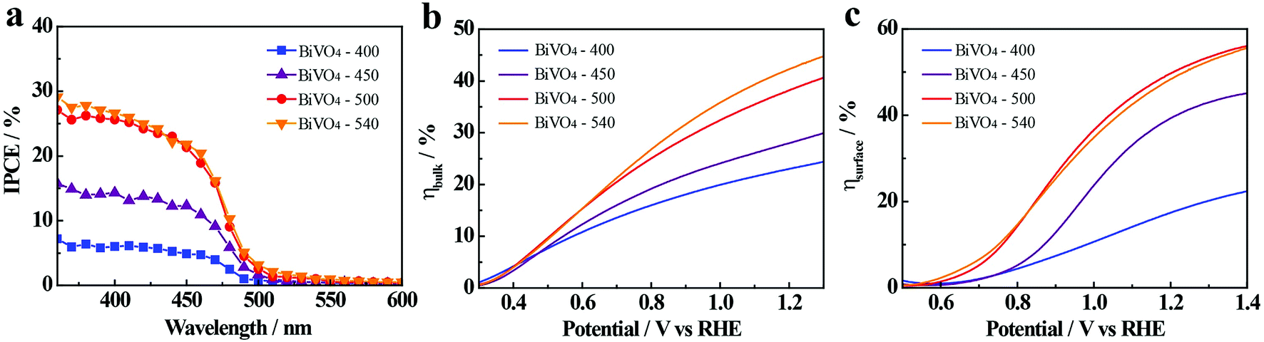 | ||
| Fig. 4 (a) The incident photon to electron conversion efficiency spectra (IPCE) of BiVO4-n samples, measured at 1.23 V vs. RHE in 0.1 M KPi buffer. Charge separation efficiency (b) in the bulk and (c) on the surface. | ||
3.5 Electrochemical properties of the photoelectrodes
In order to further explain the effect of annealing temperature on the BiVO4 photoelectrodes, the efficiency of charge transport in the bulk (ηbulk) and on the surface (ηsurface) of BiVO4-n samples are determined and presented in Fig. 4b and c (detailed calculation is given in ESI†). The ηbulk values at 1.23 V vs. RHE are 24%, 29%, 35% and 39% for BiVO4-400, BiVO4-450, BiVO4-500 and BiVO4-540, respectively, showing an increasing trend with the increase in annealing temperature. Increased bulk separation efficiency with increased annealing temperature is likely due to better crystallinity and increased grain size of BiVO4, which decrease recombination defects in the bulk and inside the grains. ηsurface is also improved by high-temperature annealing, with the values at 1.23 V vs. RHE being 19%, 41%, 51%, and 50% for BiVO4-400, BiVO4-450, BiVO4-500 and BiVO4-540, respectively. Increased surface separation efficiency is likely due to the previously discussed crystal properties that reduce charge recombination centers on the surface of BiVO4 thin film photoelectrodes. However, the insignificant difference of ηsurface between BiVO4-500 and BiVO4-540 deserves further attention.Electrochemical double-layer capacitance (Cdl) is positively proportional to the electrochemically active sites. Since it is more convenient to measure Cdl than quantitatively characterize electrochemically active sites, Cdl of BiVO4-n samples are measured to compare the electrochemically active surface areas of these samples. Cdl is measured through cyclic voltammetry (CV) potentiostatic scans in a non-faradaic potential region with different scan rates ranging from 20 to 180 mV s−1 (Fig. S12 and S13†). The potential range is 0.23–0.36 V vs. RHE for light condition and 0.47–0.6 V vs. RHE for dark. In dark, the Cdl is determined to be 0.0074, 0.0035, 0.0019, and 0.0006 mF cm−2 for BiVO4-400, BiVO4-450, BiVO4-500, and BiVO4-540, respectively (Fig. 5a). Therefore, the BiVO4 samples prepared at lower temperatures possess higher electrochemically active surface areas compared to the BiVO4 samples prepared at higher temperature. The higher electrochemically active surface areas lead to high electrocatalytic activity, which contributes to the cathodic shift of the onset potential under dark condition (Fig. 3d).
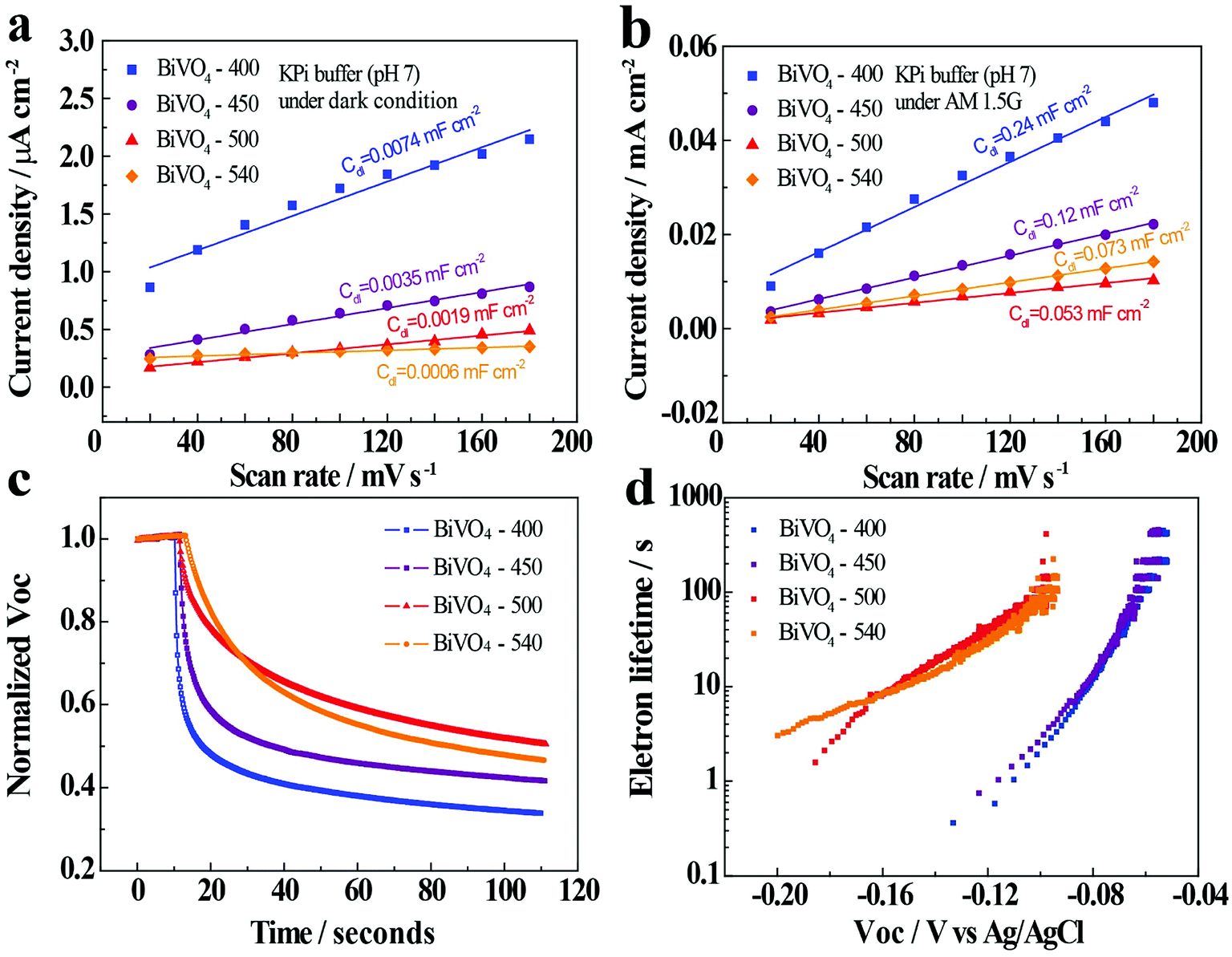 | ||
| Fig. 5 Current density (J = 0.5 × (Ja − Jc)) as a function of scan rates in (a) dark and (b) in AM 1.5G illuminated conditions. Ja and Jc present the anodic and cathodic current densities recorded at 0.54 V vs. RHE under dark and 0.3 V vs. RHE under illuminated conditions. (c) Normalized open-circuit photovoltage decay (Voc) curves of BiVO4-n samples in 0.1 M KPi buffer. (d) The potential dependent photoelectron lifetime plots for BiVO4-n. | ||
Meanwhile, when illuminated, the Cdl is determined to be 0.240, 0.120, 0.053, 0.073 mF cm−2 for BiVO4-400, BiVO4-450, BiVO4-500, and BiVO4-540, respectively (Fig. 5b). The Cdl values show a decreasing trend with the increase in the annealing temperature. These results are consistent with that of the dark condition. However, the increased current density in the illuminated condition exhibits an increase in the Cdl values. In other words, even though the BiVO4 samples prepared at lower temperatures produce higher electrochemically active surface areas, their photocurrents are lower than the BiVO4 samples prepared at higher temperature (Fig. 3).
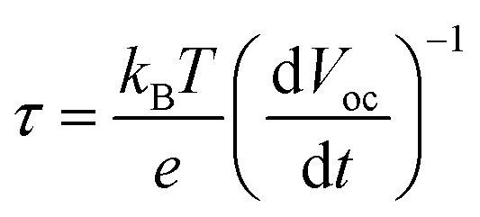
In order to better assess the contrasting effects of annealing temperatures on EC in dark and PEC performance under light illumination, open-circuit photovoltage decay (OCPVD) is measured for all the BiVO4-n samples (Fig. S14†). OCPVD consists of turning off the illumination at a steady state and monitoring the subsequent decay of open-circuit photovoltage (Voc) with time. In open-circuit condition under illumination, photo-excitation causes gradual accumulation of electrons in BiVO4 photoelectrode, which results in an upshift of the quasi-Fermi level and built-up of Voc.52,53 Since no current can flow to the external circuit, the electron accumulation is in competition against the dissipation processes, particularly, against charge recombination.54 When illumination is turned off, the charge recombination process solely dominates, leading to Voc decay. It indicates that a longer Voc decay time points to a smaller charge recombination rate of the sample. Furthermore, the normalized Voc after the light is turned off for all the BiVO4 samples are presented in Fig. 5c. The OCPVD result shows that the BiVO4 thin film photoelectrode annealed at higher temperature has the longer Voc decay time, suggesting its less charge recombination. The Voc decay rate is directly related to the photoelectron lifetime:
 | (4) |
4. Conclusions
The results of this work show that the crystallinity of the BiVO4 thin film electrodes is improved and average grain size is increased with the increase in the annealing temperature. A lower annealing temperature produces more electrochemically active sites, which is beneficial to EC performance under dark condition, while a higher annealing temperature leads to less electron–hole recombination and a better PEC performance under illumination. This work provides insights into the effects of annealing temperature in BiVO4 thin film photoelectrodes, highlights the importance of controlling annealing temperature of BiVO4 for the benefit of enhancing performance, and is thus significant to the future development of metal oxide semiconductor-based thin film photoelectrodes.Conflicts of interest
There are no conflicts to declare.Acknowledgements
This project is based upon work supported by the King Abdullah University Science and Technology (KAUST) CCF fund, awarded to Water Desalination and Reuse Center (WDRC). The authors are grateful to other members of the KAUST Environmental Nanotechnology group for their insightful discussions.References
- Y. Bai, I. Mora-Seró, F. De Angelis, J. Bisquert and P. Wang, Titanium Dioxide Nanomaterials for Photovoltaic Applications, Chem. Rev., 2014, 114(19), 10095–10130 CrossRef PubMed.
- D. Kang, T. W. Kim, S. R. Kubota, A. C. Cardiel, H. G. Cha and K.-S. Choi, Electrochemical Synthesis of Photoelectrodes and Catalysts for Use in Solar Water Splitting, Chem. Rev., 2015, 115(23), 12839–12887 CrossRef PubMed.
- N. S. Lewis, Toward Cost-Effective Solar Energy Use, Science, 2007, 315(5813), 798–801 CrossRef PubMed.
- M. G. Walter, E. L. Warren, J. R. McKone, S. W. Boettcher, Q. Mi, E. A. Santori and N. S. Lewis, Solar Water Splitting Cells, Chem. Rev., 2010, 110(11), 6446–6473 CrossRef PubMed.
- D. Das, J. Plazas-Tuttle, I. V. Sabaraya, S. S. Jain, T. Sabo-Attwood and N. B. Saleh, An elegant method for large scale synthesis of metal oxide-carbon nanotube nanohybrids for nano-environmental application and implication studies, Environ. Sci.: Nano, 2017, 4(1), 60–68 RSC.
- Y. Park, K. J. McDonald and K.-S. Choi, Progress in bismuth vanadate photoanodes for use in solar water oxidation, Chem. Soc. Rev., 2013, 42(6), 2321–2337 RSC.
- S. Tokunaga, H. Kato and A. Kudo, Selective Preparation of Monoclinic and Tetragonal BiVO4 with Scheelite Structure and Their Photocatalytic Properties, Chem. Mater., 2001, 13(12), 4624–4628 CrossRef.
- Y. Liang, T. Tsubota, L. P. A. Mooij and R. van de Krol, Highly Improved Quantum Efficiencies for Thin Film BiVO4 Photoanodes, J. Phys. Chem. C, 2011, 115(35), 17594–17598 CrossRef.
- F. F. Abdi and R. van de Krol, Nature and Light Dependence of Bulk Recombination in Co-Pi-Catalyzed BiVO4 Photoanodes, J. Phys. Chem. C, 2012, 116(17), 9398–9404 CrossRef.
- X. Chang, T. Wang, P. Zhang, J. Zhang, A. Li and J. Gong, Enhanced Surface Reaction Kinetics and Charge Separation of p–n Heterojunction Co3O4/BiVO4 Photoanodes, J. Am. Chem. Soc., 2015, 137(26), 8356–8359 CrossRef PubMed.
- L. Zhou, C. Zhao, B. Giri, P. Allen, X. Xu, H. Joshi, Y. Fan, L. V. Titova and P. M. Rao, High Light Absorption and Charge Separation Efficiency at Low Applied Voltage from Sb-Doped SnO2/BiVO4 Core/Shell Nanorod-Array Photoanodes, Nano Lett., 2016, 16(6), 3463–3474 CrossRef PubMed.
- J. Su, L. Guo, N. Bao and C. A. Grimes, Nanostructured WO3/BiVO4 Heterojunction Films for Efficient Photoelectrochemical Water Splitting, Nano Lett., 2011, 11(5), 1928–1933 CrossRef PubMed.
- B.-Y. Cheng, J.-S. Yang, H.-W. Cho and J.-J. Wu, Fabrication of an Efficient BiVO4–TiO2 Heterojunction Photoanode for Photoelectrochemical Water Oxidation, ACS Appl. Mater. Interfaces, 2016, 8(31), 20032–20039 CrossRef PubMed.
- Y. Hu, D. Li, Y. Zheng, W. Chen, Y. He, Y. Shao, X. Fu and G. Xiao, BiVO4/TiO2 nanocrystalline heterostructure: a wide spectrum responsive photocatalyst towards the highly efficient decomposition of gaseous benzene, Appl. Catal., B, 2011, 104(1), 30–36 CrossRef.
- X. Zheng, B. Sciacca, E. C. Garnett and L. Zhang, AgFeS2-Nanowire-Modified BiVO4 Photoanodes for Photoelectrochemical Water Splitting, ChemPlusChem, 2016, 81(10), 1075–1082 CrossRef.
- H. S. Park, K. E. Kweon, H. Ye, E. Paek, G. S. Hwang and A. J. Bard, Factors in the Metal Doping of BiVO4 for Improved Photoelectrocatalytic Activity as Studied by Scanning Electrochemical Microscopy and First-Principles Density-Functional Calculation, J. Phys. Chem. C, 2011, 115(36), 17870–17879 CrossRef.
- S. K. Cho, H. S. Park, H. C. Lee, K. M. Nam and A. J. Bard, Metal Doping of BiVO4 by Composite Electrodeposition with Improved Photoelectrochemical Water Oxidation, J. Phys. Chem. C, 2013, 117(44), 23048–23056 CrossRef.
- K. P. S. Parmar, H. J. Kang, A. Bist, P. Dua, J. S. Jang and J. S. Lee, Photocatalytic and Photoelectrochemical Water Oxidation over Metal-Doped Monoclinic BiVO4 Photoanodes, ChemSusChem, 2012, 5(10), 1926–1934 CrossRef PubMed.
- L. Zhang, E. Reisner and J. J. Baumberg, Al-doped ZnO inverse opal networks as efficient electron collectors in BiVO4 photoanodes for solar water oxidation, Energy Environ. Sci., 2014, 7(4), 1402–1408 RSC.
- L. Zhang, L. O. Herrmann and J. J. Baumberg, Size Dependent Plasmonic Effect on BiVO4 Photoanodes for Solar Water Splitting, Sci. Rep., 2015, 5, 16660 CrossRef PubMed.
- L. Zhang, C.-Y. Lin, V. K. Valev, E. Reisner, U. Steiner and J. J. Baumberg, Plasmonic Enhancement in BiVO4 Photonic Crystals for Efficient Water Splitting, Small, 2014, 10(19), 3970–3978 CrossRef PubMed.
- Y. Deng, L. Tang, C. Feng, G. Zeng, J. Wang, Y. Zhou, Y. Liu, B. Peng and H. Feng, Construction of plasmonic Ag modified phosphorous-doped ultrathin g-C3N4 nanosheets/BiVO4 photocatalyst with enhanced visible-near-infrared response ability for ciprofloxacin degradation, J. Hazard. Mater., 2018, 344, 758–769 CrossRef PubMed.
- Z. Wei, D. Benlin, Z. Fengxia, T. Xinyue, X. Jiming, Z. Lili, L. Shiyin, D. Y. C. Leung and C. Sun, A novel 3D plasmonic p-n heterojunction photocatalyst: Ag nanoparticles on flower-like p-Ag2S/n-BiVO4 and its excellent photocatalytic reduction and oxidation activities, Appl. Catal., B, 2018, 229, 171–180 CrossRef.
- D. Wang, R. Li, J. Zhu, J. Shi, J. Han, X. Zong and C. Li, Photocatalytic Water Oxidation on BiVO4 with the Electrocatalyst as an Oxidation Cocatalyst: Essential Relations between Electrocatalyst and Photocatalyst, J. Phys. Chem. C, 2012, 116(8), 5082–5089 CrossRef.
- L. Xia, J. Bai, J. Li, Q. Zeng, L. Li and B. Zhou, High-performance BiVO4 photoanodes cocatalyzed with an ultrathin α-Fe2O3 layer for photoelectrochemical application, Appl. Catal., B, 2017, 204(suppl. C), 127–133 CrossRef.
- T. Palaniselvam, L. Shi, G. Mettela, D. H. Anjum, R. Li, K. P. Katuri, P. E. Saikaly and P. Wang, Vastly Enhanced BiVO4 Photocatalytic OER Performance by NiCoO2 as Cocatalyst, Adv. Mater. Interfaces, 2017, 4(19), 1700540 CrossRef.
- M. Kan, D. Xue, A. Jia, X. Qian, D. Yue, J. Jia and Y. Zhao, A highly efficient nanoporous BiVO4 photoelectrode with enhanced interface charge transfer Co-catalyzed by molecular catalyst, Appl. Catal., B, 2018, 225, 504–511 CrossRef.
- S. M. Thalluri, C. Martinez Suarez, M. Hussain, S. Hernandez, A. Virga, G. Saracco and N. Russo, Evaluation of the Parameters Affecting the Visible-Light-Induced Photocatalytic Activity of Monoclinic BiVO4 for Water Oxidation, Ind. Eng. Chem. Res., 2013, 52(49), 17414–17418 CrossRef.
- A. Chemseddine, K. Ullrich, T. Mete, F. F. Abdi and R. van de Krol, Solution-processed multilayered BiVO4 photoanodes: influence of intermediate heat treatments on the photoactivity, J. Mater. Chem. A, 2016, 4(5), 1723–1728 RSC.
- S. Hernández, G. Gerardi, K. Bejtka, A. Fina and N. Russo, Evaluation of the charge transfer kinetics of spin-coated BiVO4 thin films for sun-driven water photoelectrolysis, Appl. Catal., B, 2016, 190(suppl. C), 66–74 CrossRef.
- S. N. F. M. Nasir, M. A. M. Teridi, M. Ebadi, J. S. Sagu, M. Y. Sulaiman, N. A. Ludin and M. A. Ibrahim, Annealing effect on the photoelectrochemical properties of BiVO4 thin film electrodes, Malaysian Journal of Analytical Sciences, 2015, 19(6), 1250–1255 Search PubMed.
- A. Khorsand Zak, W. H. Abd. Majid, M. E. Abrishami and R. Yousefi, X-ray analysis of ZnO nanoparticles by Williamson–Hall and size–strain plot methods, Solid State Sci., 2011, 13(1), 251–256 CrossRef.
- P. Brack, J. S. Sagu, T. A. N. Peiris, A. McInnes, M. Senili, K. G. U. Wijayantha, F. Marken and E. Selli, Aerosol-Assisted CVD of Bismuth Vanadate Thin Films and Their Photoelectrochemical Properties, Chem. Vap. Deposition, 2015, 21(1–2-3), 41–45 CrossRef.
- N. Butenko, A. I. Tomaz, O. Nouri, E. Escribano, V. Moreno, S. Gama, V. Ribeiro, J. P. Telo, J. C. Pesssoa and I. Cavaco, DNA cleavage activity of VIVO(acac)2 and derivatives, J. Inorg. Biochem., 2009, 103(4), 622–632 CrossRef PubMed.
- G. P. Nagabhushana, G. Nagaraju and G. T. Chandrappa, Synthesis of bismuth vanadate: its application in H2 evolution and sunlight-driven photodegradation, J. Mater. Chem. A, 2013, 1(2), 388–394 RSC.
- J. H. Nobbs, Kubelka–Munk Theory and the Prediction of Reflectance, Rev. Prog. Color. Relat. Top., 1985, 15(1), 66–75 CrossRef.
- A. Kudo, K. Omori and H. Kato, A Novel Aqueous Process for Preparation of Crystal Form-Controlled and Highly Crystalline BiVO4 Powder from Layered Vanadates at Room Temperature and Its Photocatalytic and Photophysical Properties, J. Am. Chem. Soc., 1999, 121(49), 11459–11467 CrossRef.
- Z. Zhao, Z. Li and Z. Zou, Electronic structure and optical properties of monoclinic clinobisvanite BiVO4, Phys. Chem. Chem. Phys., 2011, 13(10), 4746–4753 RSC.
- D. Wang, H. Jiang, X. Zong, Q. Xu, Y. Ma, G. Li and C. Li, Crystal Facet Dependence of Water Oxidation on BiVO4 Sheets under Visible Light Irradiation, Chem.–Eur. J., 2011, 17(4), 1275–1282 CrossRef PubMed.
- S. M. Thalluri, C. Martinez Suarez, S. Hernández, S. Bensaid, G. Saracco and N. Russo, Elucidation of important parameters of BiVO4 responsible for photo-catalytic O2 evolution and insights about the rate of the catalytic process, Chem. Eng. J., 2014, 245(suppl. C), 124–132 CrossRef.
- S. Wang, P. Chen, J.-H. Yun, Y. Hu and L. Wang, An Electrochemically Treated BiVO4 Photoanode for Efficient Photoelectrochemical Water Splitting, Angew. Chem., 2017, 129(29), 8620–8624 CrossRef.
- F. F. Abdi, L. Han, A. H. M. Smets, M. Zeman, B. Dam and R. van de Krol, Efficient solar water splitting by enhanced charge separation in a bismuth vanadate-silicon tandem photoelectrode, Nat. Commun., 2013, 4, 2195 CrossRef PubMed.
- J. K. Cooper, S. Gul, F. M. Toma, L. Chen, Y.-S. Liu, J. Guo, J. W. Ager, J. Yano and I. D. Sharp, Indirect Bandgap and Optical Properties of Monoclinic Bismuth Vanadate, J. Phys. Chem. C, 2015, 119(6), 2969–2974 CrossRef.
- Z. Zhang, X. Yang, M. N. Hedhili, E. Ahmed, L. Shi and P. Wang, Microwave-Assisted Self-Doping of TiO2 Photonic Crystals for Efficient Photoelectrochemical Water Splitting, ACS Appl. Mater. Interfaces, 2014, 6(1), 691–696 CrossRef PubMed.
- X. Ren, Z. Yang, D. Yang, X. Zhang, D. Cui, Y. Liu, Q. Wei, H. Fan and S. Liu, Modulating crystal grain size and optoelectronic properties of perovskite films for solar cells by reaction temperature, Nanoscale, 2016, 8(6), 3816–3822 RSC.
- H. Gong, N. Freudenberg, M. Nie, R. v. d. Krol and K. Ellmer, BiVO4 photoanodes for water splitting with high injection efficiency, deposited by reactive magnetron co-sputtering, AIP Adv., 2016, 6(4), 045108 CrossRef.
- D. K. Zhong, S. Choi and D. R. Gamelin, Near-Complete Suppression of Surface Recombination in Solar Photoelectrolysis by “Co-Pi” Catalyst-Modified W:BiVO4, J. Am. Chem. Soc., 2011, 133(45), 18370–18377 CrossRef PubMed.
- S. K. Choi, W. Choi and H. Park, Solar water oxidation using nickel-borate coupled BiVO4 photoelectrodes, Phys. Chem. Chem. Phys., 2013, 15(17), 6499–6507 RSC.
- F. Le Formal, K. Sivula and M. Grätzel, The Transient Photocurrent and Photovoltage Behavior of a Hematite Photoanode under Working Conditions and the Influence of Surface Treatments, J. Phys. Chem. C, 2012, 116(51), 26707–26720 CrossRef.
- L. M. Peter, Energetics and kinetics of light-driven oxygen evolution at semiconductor electrodes: the example of hematite, J. Solid State Electrochem., 2013, 17(2), 315–326 CrossRef.
- Z. Zhang, L. Zhang, M. N. Hedhili, H. Zhang and P. Wang, Plasmonic Gold Nanocrystals Coupled with Photonic Crystal Seamlessly on TiO2 Nanotube Photoelectrodes for Efficient Visible Light Photoelectrochemical Water Splitting, Nano Lett., 2013, 13(1), 14–20 CrossRef PubMed.
- R. P. Antony, P. S. Bassi, F. F. Abdi, S. Y. Chiam, Y. Ren, J. Barber, J. S. C. Loo and L. H. Wong, Electrospun Mo-BiVO4 for Efficient Photoelectrochemical Water Oxidation: Direct Evidence of Improved Hole Diffusion Length and Charge separation, Electrochim. Acta, 2016, 211(suppl. C), 173–182 CrossRef.
- Z. Zhang and P. Wang, Optimization of photoelectrochemical water splitting performance on hierarchical TiO2 nanotube arrays, Energy Environ. Sci., 2012, 5(4), 6506–6512 RSC.
- N. Baram and Y. Ein-Eli, Electrochemical Impedance Spectroscopy of Porous TiO2 for Photocatalytic Applications, J. Phys. Chem. C, 2010, 114(21), 9781–9790 CrossRef.
Footnote |
| † Electronic supplementary information (ESI) available. See DOI: 10.1039/c8ra04887h |
| This journal is © The Royal Society of Chemistry 2018 |