
 Open Access Article
 This Open Access Article is licensed under a Creative Commons Attribution-Non Commercial 3.0 Unported Licence
Localized incorporation of cesium ions to improve formamidinium lead iodide layers in perovskite solar cells†
Yebin Xuea,
Jiaqi Tiana,
Haiyue Wanga,
Honggang Xiea,
Shanshan Zhua,
Bo Zhenga,
Chunxiao Gaob and
Xizhe Liu *a
*a
aInstitute of Atomic and Molecular Physics, Jilin Provincial Key Laboratory of Applied Atomic and Molecular Spectroscopy, Jilin University, Changchun, 130012, China. E-mail: liu_xizhe@jlu.edu.cn
bState Key Laboratory for Superhard Materials, Jilin University, Changchun, 130012, China
First published on 18th July 2018
Abstract
For the perovskite solar cells with formamidinium lead iodide (FAPbI3) as a light harvester, cesium ions (Cs+) can be used to stabilize the perovskite crystal structure of FAPbI3. However, the incorporation of Cs+ ions usually reduces the grain size and degrades the crystallization of FAPbI3 layers, and this is harmful to the photovoltaic performance of solar cells. In this work, we incorporate Cs+ ions into FAPbI3 layers using the interfacial doping method, which is different from the mixed solution doping method in previous reports. Elemental analysis indicates that Cs+ dopants cannot be detected at the outer surfaces of perovskite layers, and the majority of Cs+ dopants should be localized in the vicinity of TiO2/perovskite interfaces, which is remarkably different from the distribution of Cs+ dopants in the perovskite layers prepared using the mixed solution doping method. It is found that interfacial doping method can avoid the blue shift of the light absorption edge and can improve the crystallization of FAPbI3 layers. For the optimized conditions, CsxFA1−xPbI3 solar cells prepared using the interfacial doping method achieve a power conversion efficiency (PCE) of 17.1%, which is better than the PCE of CsxFA1−xPbI3 devices prepared using the mixed solution doping method.
Introduction
Perovskite solar cells (PSCs) have become a research focus of photovoltaic devices for their solution processability and efficient solar-to-electric conversion.1–4 Their excellent photovoltaic performance comes from the application of organic lead halides as light harvesters, which have the perovskite structure of ABX3.5,6 Although organic lead iodides based on formamidinium ions (HC(NH2)2+, FA+) are excellent light harvesting materials for photovoltaic devices,7–10 high quality α-phase FAPbI3 layers are difficult to fabricate using solution deposition.11,12 As a result of a large tolerance factor for α-phase FAPbI3, the yellow δ-phase with a hexagonal structure is the stable crystal structure for FAPbI3 at room temperature. To stabilize the α-phase structure of FAPbI3, the FA+ ions of FAPbI3 can be partially substituted with univalent cations with small sizes.13–15Several reports indicate that partial substitution of FA+ ions with cesium (Cs+) ions can eliminate the tension in FAPbI3 crystals, and this substantially improves the photovoltaic performance and stability of devices.16–19 Although Cs+ doped FAPbI3 (CsxFA1−xPbI3) exhibits some promising properties, the PCEs of devices are still relatively low compared to the state-of-the-art records of PSCs. It is found that the incorporation of Cs+ ions intensely increases the density of crystal nuclei in the film formation process, which leads to a remarkable decrease in grain size in perovskite layers.20 The small grain size results in the enhancement of the recombination process in PSCs.21,22 On the other hand, the bandgap of CsxFA1−xPbI3 increases with the increase in Cs+ ions.16,17 Therefore, the incorporation of Cs+ ions also leads to a blue shift in the light absorption edge for perovskite layers, which is harmful to the utilization of solar light.
Cs+ ion doping is often implemented by incorporating CsI into the precursor solutions of FAPbI3.16–19 In this doping method, Cs+ ions tend to be dispersed in the entire film at all depths. Interfacial diffusion is another widely used method for incorporating dopants, and its doping profile is mainly localized in the vicinity of doping interfaces.23–25 This localized doping method can be adopted for preparing Cs+ doped FAPbI3 layers, which are composed of a Cs+ doped underlayer and an undoped capping layer. The undoped part of the perovskite layers tends to preserve the original bandgap of FAPbI3, which prevents the blue shift of light absorption by Cs+ ion incorporation. It is also noted that this kind of doping profile likely generates a remarkable bandgap gradient in the vicinity of interfaces. The gradient structure of the bandgap can provide an additional driving force for the separation of photo-generated electrons and holes, and this is named the quasi-electric field effect.26–28 Recent reports indicate that engineering the anion gradient at the outer surface of perovskite layers suppresses the recombination process of perovskite solar cells.29–31 Therefore, this localized doping method should be a promising way to promote the photovoltaic performance of CsxFA1−xPbI3 solar cells.
In this work, we fabricated CsxFA1−xPbI3 layers using the interfacial doping method as the light harvester of perovskite solar cells. By this localized Cs+ doping, the crystallization was improved and the light absorption range was preserved for these perovskite layers. After optimizing the quantity of dopants, the recombination process of PSCs was suppressed and the power conversion efficiency (PCE) can be promoted.
Experimental
Firstly, FTO glass was etched using a 1064 nm laser and it was ultrasonically cleaned using acetone and ethanol. Then, a 30 nm TiO2 blocking layer was deposited on the cleaned FTO using spray pyrolysis of 2.0 mL 0.05 M Ti(OPr)2(acetylacetonate)2 solution using oxygen as the carrying gas at 450 °C. Then a mesoporous TiO2 film was deposited using spin-coating with an ethanol diluted TiO2 paste (18NRT, Dyesol) solution at 5000 rpm for 30 s. The mass ratio of original TiO2 paste to ethanol is 1![[thin space (1/6-em)]](https://www.rsc.org/images/entities/char_2009.gif) :6. These samples were dried and sintered at 80 °C for 30 min, 100 °C for 30 min, 350 °C for 30 min, and 500 °C for 30 min sequentially. Then CsI doping layers were deposited using spin-coating at 4000 rpm for 30 s with 50, 100, and 200 mg mL−1 CsI in N,N-dimethylformamide (DMF) solutions, which are labelled as CsI50, CsI100 and CsI200 respectively. Undoped samples without CsI doping layers were also prepared as the reference. For preparing formamidinium perovskite layers, PbI2 films were deposited on the samples using spin-coating with 462 mg mL−1 PbI2 in DMF solution at 4000 rpm for 30 s. After preheating at 160 °C for 10 min on a hot plate, 60 μL 50 mg mL−1 FAI in isopropanol solution was sprayed on the top of the PbI2 film using a nitrogen gas atomizing spray nozzle at 160 °C. After the interface reaction process, the film was washed with isopropanol and annealed at 160 °C for another 10 min. We also fabricated Cs+ doped FAPbI3 layers by directly spin-coating a mixed solution of 0.1 M CsI and 1.0 M PbI2 in DMF, which acts as the precursor layer in the mixed solution doping method.19 When cooled to room temperature, hole transport material layers were prepared using spin-coating of a solution containing 72.3 mg spiro-MeOTAD, 28.5 μL 4-tert-butylpyridine and 18.5 μL lithium bis(trifluoromethanesulfonyl)imide solution (520 mg mL−1 in acetonitrile) in 1 mL of chlorobenzene as the solvent at 4000 rpm for 30 s. After being aged in a brown desiccator for 12 hours, Au electrodes were deposited using vacuum thermal evaporation.
:6. These samples were dried and sintered at 80 °C for 30 min, 100 °C for 30 min, 350 °C for 30 min, and 500 °C for 30 min sequentially. Then CsI doping layers were deposited using spin-coating at 4000 rpm for 30 s with 50, 100, and 200 mg mL−1 CsI in N,N-dimethylformamide (DMF) solutions, which are labelled as CsI50, CsI100 and CsI200 respectively. Undoped samples without CsI doping layers were also prepared as the reference. For preparing formamidinium perovskite layers, PbI2 films were deposited on the samples using spin-coating with 462 mg mL−1 PbI2 in DMF solution at 4000 rpm for 30 s. After preheating at 160 °C for 10 min on a hot plate, 60 μL 50 mg mL−1 FAI in isopropanol solution was sprayed on the top of the PbI2 film using a nitrogen gas atomizing spray nozzle at 160 °C. After the interface reaction process, the film was washed with isopropanol and annealed at 160 °C for another 10 min. We also fabricated Cs+ doped FAPbI3 layers by directly spin-coating a mixed solution of 0.1 M CsI and 1.0 M PbI2 in DMF, which acts as the precursor layer in the mixed solution doping method.19 When cooled to room temperature, hole transport material layers were prepared using spin-coating of a solution containing 72.3 mg spiro-MeOTAD, 28.5 μL 4-tert-butylpyridine and 18.5 μL lithium bis(trifluoromethanesulfonyl)imide solution (520 mg mL−1 in acetonitrile) in 1 mL of chlorobenzene as the solvent at 4000 rpm for 30 s. After being aged in a brown desiccator for 12 hours, Au electrodes were deposited using vacuum thermal evaporation.
Scanning electron microscopy (SEM) was investigated using a FEI-MAGELLAN 400 scanning electron microscope. X-ray diffraction (XRD) patterns were obtained using a Rigaku D/max-2550 X-ray diffractometer. The UV-vis absorption spectra were recorded with a L5S UV-vis spectrophotometer in the 500–900 nm wavelength range. Photocurrent density–photovoltage characteristics were recorded from 1.10 V to 0 V using a CHI660 electrochemical workstation. The active area of the solar cells is 0.16 cm2, which is defined by a mask. The AM1.5 illumination was provided by a 3A class solar simulator (UHE-16, ScienceTech Inc.), which was calibrated to one sun by a KG5-filtered Si reference solar cell (certificated by VLSI Standards Inc., traceable to the National Renewable Energy Laboratory). Photoluminescence (PL) spectra were detected using a CCD detector (PIXIS256BR, Princeton Instruments Inc.), and the excitation wavelength was 532 nm, provided by a low-noise solid-state laser (MLL-III-532). Impedance spectra were measured under constant illumination conditions over a frequency range from 1 MHz to 1 Hz using a CHI660 electrochemical workstation. The constant illumination was provided by a white LED lamp array. Inductively coupled plasma (ICP) analysis was investigated using an Agilent 7500a inductively coupled plasma source mass spectrometer. X-ray photoelectron spectroscopy (XPS) was performed using an X-ray photoelectron spectrometer (Thermo Scientific Escalab 250Xi).
Results and discussion
As shown in Fig. 1a, the PbI2 films without CsI doping layers are composed of irregular nanoparticles. However, the morphology of PbI2 films change remarkably by inserting CsI doping layers between TiO2 layers and PbI2 layers. For the doping layers produced using the 50 mg mL−1 CsI solution (CsI50 layers), PbI2 films are composed of nanorod-like grains. By increasing the concentration of CsI solutions to 100 mg mL−1 and 200 mg mL−1 (CsI100 and CsI200 layers), pinhole defects emerge and increase in the PbI2 layers (Fig. 1c and d). These results indicate that CsI doping layers can modify the morphology of PbI2 layers. As perovskite layers are prepared by the reaction between PbI2 layers and the FAI precursor, the morphology of PbI2 layers also affects the formation of perovskite layers. Fig. 1e shows the XRD patterns of PbI2 films without and with different CsI doping layers. CsI50 doping layers lead to a moderate reduction in the intensity of the PbI2 diffraction peak at 12.8°. After further increasing the quantity of CsI dopants (CsI100 and CsI200), the intensity of the PbI2 diffraction peaks decrease remarkably. This result indicates that the incorporation of CsI doping layers can decrease the crystallization of PbI2 layers. Low crystallization of PbI2 layers favours the accessibility of organic ammonium iodide to inner lead sites, and this can be beneficial to the crystal growth of perovskite layers.32,33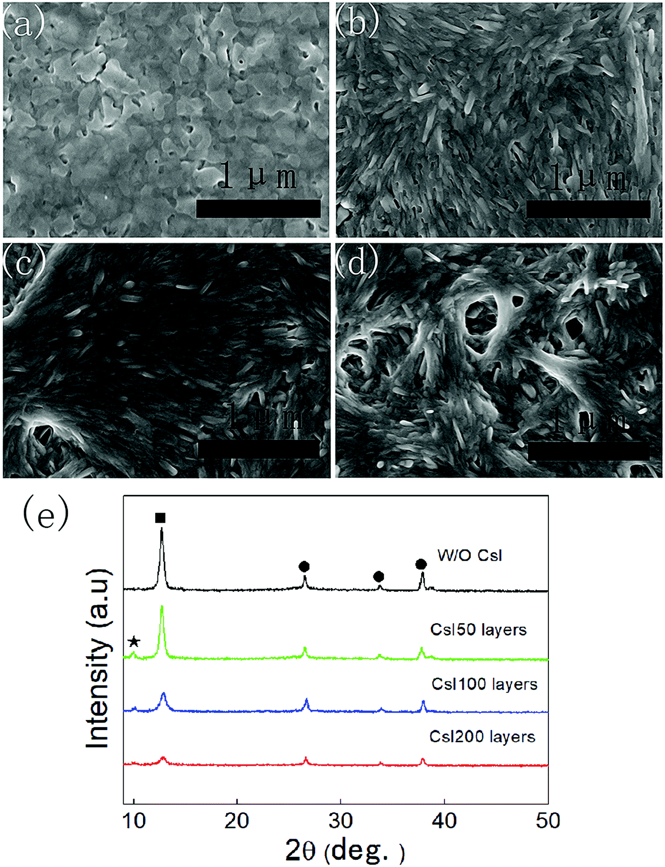 | ||
| Fig. 1 Top-view SEM images of PbI2 layers without (a) and with CsI50 (b), CsI100 (c), CsI200 (d) doping layers, and (e) X-ray diffraction patterns of PbI2 layers without and with different CsI doping layers, where the diffraction peaks of FTO, PbI2 and δ-CsPbI3 are labelled with solid circles, solid squares and solid asterisks, respectively. | ||
Fig. 2 shows the morphology of perovskite layers from different PbI2 layers using SEM measurements. The perovskite layer produced from the undoped PbI2 layer is composed of small grains with the average size of 150 nm (Fig. 2a). For the PbI2 layers with CsI50 doping layers, the average grain size of perovskite layers remarkably increases to 420 nm (Fig. 2b), and the perovskite layers retain a compact structure. It means that PbI2 layers with nanorod like grains facilitate the growth of perovskite grains, which is beneficial for producing high quality perovskite layers. After further increasing the quantity of the CsI dopant, the average grain size of formamidinium perovskite layers continuously increases to 450 nm (Fig. 2c) and 500 nm (Fig. 2d), while pinhole defects emerge in the perovskite layers. These pinholes are likely related to the holes in PbI2 layers in Fig. 1c and d. Although small holes in PbI2 layers can be eliminated by the volume expansion in the formation of perovskite layers, big holes still lead to pinhole defects in perovskite layers. These pinhole defects are usually harmful to the device performance.
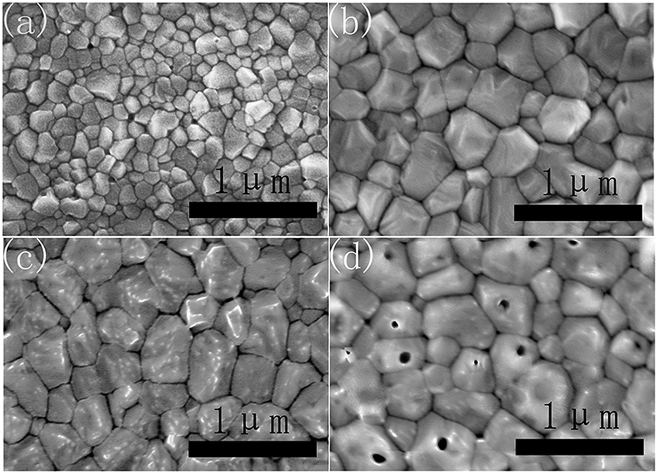 | ||
| Fig. 2 Top-view SEM images of perovskite layers without (a) and with CsI50 (b), CsI100 (c), and CsI200 (d) doping layers. | ||
The XRD patterns of these four different perovskite layers are shown in Fig. 3a, and all of the XRD diffraction peaks can be assigned to CsxFA1−xPbI3 with α-phase and FTO substrates.16,17 It means that formamidinium perovskite layers with pure α-phases can be prepared using the two step method. Moreover, the full width of half maximum (FWHM) of (110) diffraction peaks in these formamidinium perovskite layers is extracted from Fig. 3a, and these are summarized in Fig. 3b. The FWHM of formamidinium perovskite layers without CsI doping is 0.301°. By introducing CsI50 doping layers, the FWHM of formamidinium perovskite layers decreases to 0.241°. When the quantity of CsI dopants further increases (CsI100 and CsI200), the FWHM of formamidinium perovskite layers moderately increase to 0.260° and 0.272°, respectively. The broadening of XRD peaks usually comes from the low quality of crystallization, and consequently a small FWHM is related to the high quality of perovskite layers. Therefore, the optimized doping layer of CsI50 promotes the crystallization of formamidinium perovskite layers. In previous reports, CsxFA1−xPbI3 layers are usually obtained by directly adding CsI dopants into the precursor solution, and CsI dopants usually lead to a decrease in grain size and crystallization in FAPbI3 layers. In contrast, these interfacial doping layers can remarkably increase the grain size and crystallization of FAPbI3 layers, which should be a promising doping method for CsxFA1−xPbI3 solar cells.
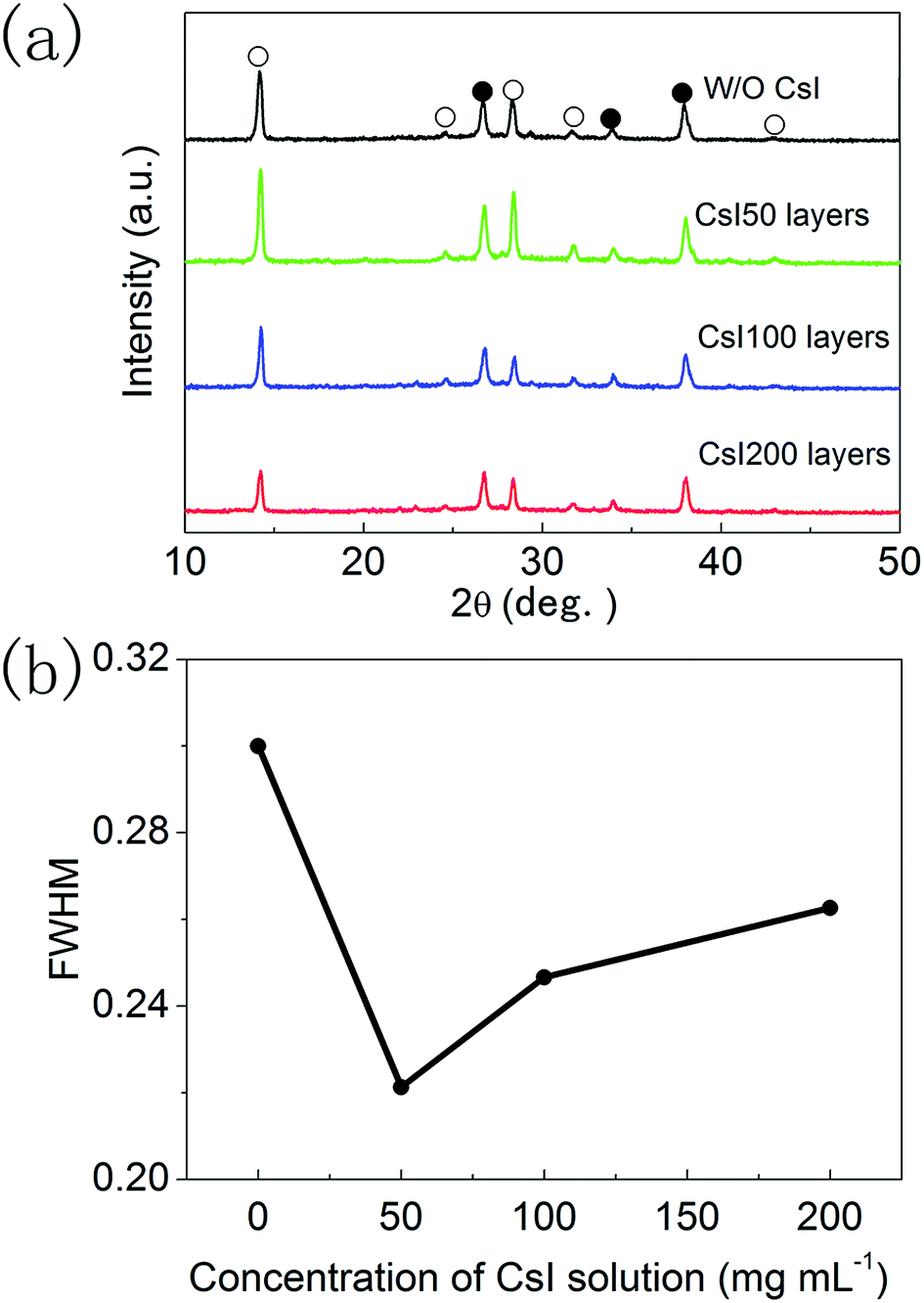 | ||
| Fig. 3 (a) X-ray diffraction patterns of perovskite layers without and with different CsI doping layers, and (b) FWHM of (110) diffraction peaks. Diffraction peaks of FTO and perovskite are labelled with solid circles and open circles, respectively. | ||
XRD measurements were also performed to analyse the formation of CsxFA1−xPbI3 layers prepared using the interfacial doping method (Fig. 4a). After the spincoating of 1.0 M PbI2 solution on CsI doping layers, the diffraction peaks of CsI (27.9°, 39.8°) disappear, while the diffraction peak of PbI2 (12.8°) and another diffraction peak at 10.01° appear. These new diffraction peaks can be assigned to the formation of δ-CsPbI3.34,35 This means that an interdiffusion reaction between CsI layers and PbI2 layers has taken place. As the quantity of CsI is much smaller than that of PbI2, δ-CsPbI3 is likely located in the vicinity of doping interfaces. After reacting with the FAI precursor, the diffraction peaks of PbI2 and δ-CsPbI3 are eliminated and the diffraction peaks of the black α-phase perovskite materials emerged. Therefore, the precursor layers react with FAI completely and CsxFA1−xPbI3 layers with a pure α-phase structure can be obtained. It is also noted that the diffraction peaks of PbI2 and CsI can be found in the PbI2 layers prepared using the mixed solution method and the diffraction peaks of δ-CsPbI3 are not observed (Fig. S1†). The relatively homogenous distribution of CsI in PbI2 layers prepared using the mixed solution method leads to a small CsI/PbI2 ratio, which is far from the stoichiometric ratio required to form δ-CsPbI3. However, the CsI dopant mainly localizes in the vicinity of doping interfaces for the interfacial doping method, which satisfies the stoichiometric ratio to form δ-CsPbI3.
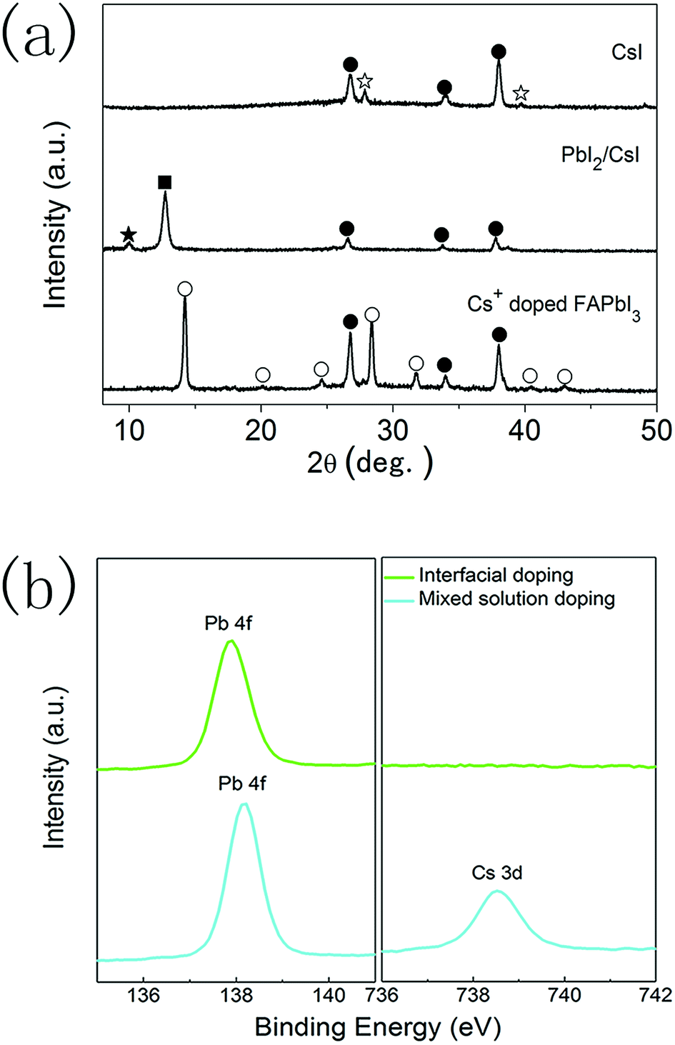 | ||
| Fig. 4 (a) X-ray diffraction patterns for the deposition process of the interfacial doping method, where diffraction peaks of FTO, CsI, PbI2, δ-CsPbI3 and α-FAPbI3 are labelled with solid circles, open asterisks, solid squares, solid asterisks and open circles, respectively. (b) XPS spectra of perovskite layers prepared using the interfacial doping and mixed solution doping methods. | ||
To further clarify the features of these CsxFA1−xPbI3 layers, elemental analysis was performed on the perovskite layers prepared using the interfacial doping method, and the CsxFA1−xPbI3 layers prepared using the mixed solution method were employed as the reference. Fig. 4b shows the X-ray photoelectron spectra (XPS) of CsxFA1−xPbI3 layers. For the sample prepared using the mixed solution method, clear peaks due to Pb and Cs elements can be distinguished. On the contrary, the XPS peak due to the Cs element cannot be detected for the CsxFA1−xPbI3 layers prepared using the interfacial doping method, which indicates a very low concentration of the Cs element at the outer surfaces of perovskite layers. ICP measurements indicate that the global doping ratio of Cs+ ions is 15.6% for the perovskite layers with CsI50 doping layers, which is far from the undetectable limit of the Cs element. As XPS spectra represent the surface properties, the remarkably different Cs+ concentration at the outer surfaces of perovskite layers confirms the different Cs+ concentration profiles at different depths by these two doping methods. The undetectable XPS signal of the Cs element implies that the majority of Cs+ ions are located in the vicinity of TiO2/perovskite interfaces for the interfacial doping method. The binding energies of Pb 4f peaks are 137.9 eV and 138.2 eV for the perovskite layers prepared using the interfacial doping method and the mixed solution method, respectively (Fig. 4b). The cesium dopant can lead to an increase in the binding energy of the Pb 4f peaks, and this is related to the change in the chemical bonding nature by the shrinkage of lattice parameters.16,17 Therefore, the relatively low binding energy of Pb 4f peaks for the sample prepared using the interfacial doping method is in accordance with the low Cs+ concentration at the outer surfaces of perovskite layers.
To explore the effect of this localized Cs+ doping on the device performance, a series of PSCs are fabricated with different CsI doping layers. Fig. 5a shows the photocurrent density–photovoltage curves of the best-performing devices and their photovoltaic parameters are summarized in Table S1.† The device without a CsI doping layer has a PCE of 13.4% with an open circuit voltage (Voc) of 1.01 V, a short-circuit current density (Jsc) of 20.1 mA cm−2, and a fill-factor of 0.66. After inserting a CsI doping layer by spincoating a 50 mg mL−1 solution, the PCE of the device is promoted to 17.1%, which comes from the simultaneous increase in Jsc (23.0 mA cm−2), Voc (1.05 V) and the fill-factor (0.71). This result indicates that a CsI doping layer can improve the performance of formamidinium perovskite solar cells, which can be related to the improvement in crystallization for perovskite layers (Fig. 2 and 3). However, further increasing the quantity of CsI dopant diminishes the device performance to 12.7% and 9.8% for the CsI100 and CsI200 doping layers, respectively. It is in accordance with the emergence of pinhole defects and degradation of crystallization in the perovskite layers by increasing the CsI quantity (Fig. 2 and 3). To evaluate the reproducibility, we performed a statistical analysis of 32 devices for undoped devices and CsI50 layers doped devices in Fig. 5b. For the devices with CsI50 doping layers, the PCEs of devices are distributed in the range from 13.5% to 17.1% with an average efficiency of about 14.9%. In contrast, the average PCE of undoped devices is located at 11.5%. This result confirms that CsI50 doped layers promote the performance of CsxFA1−xPbI3 solar cells.
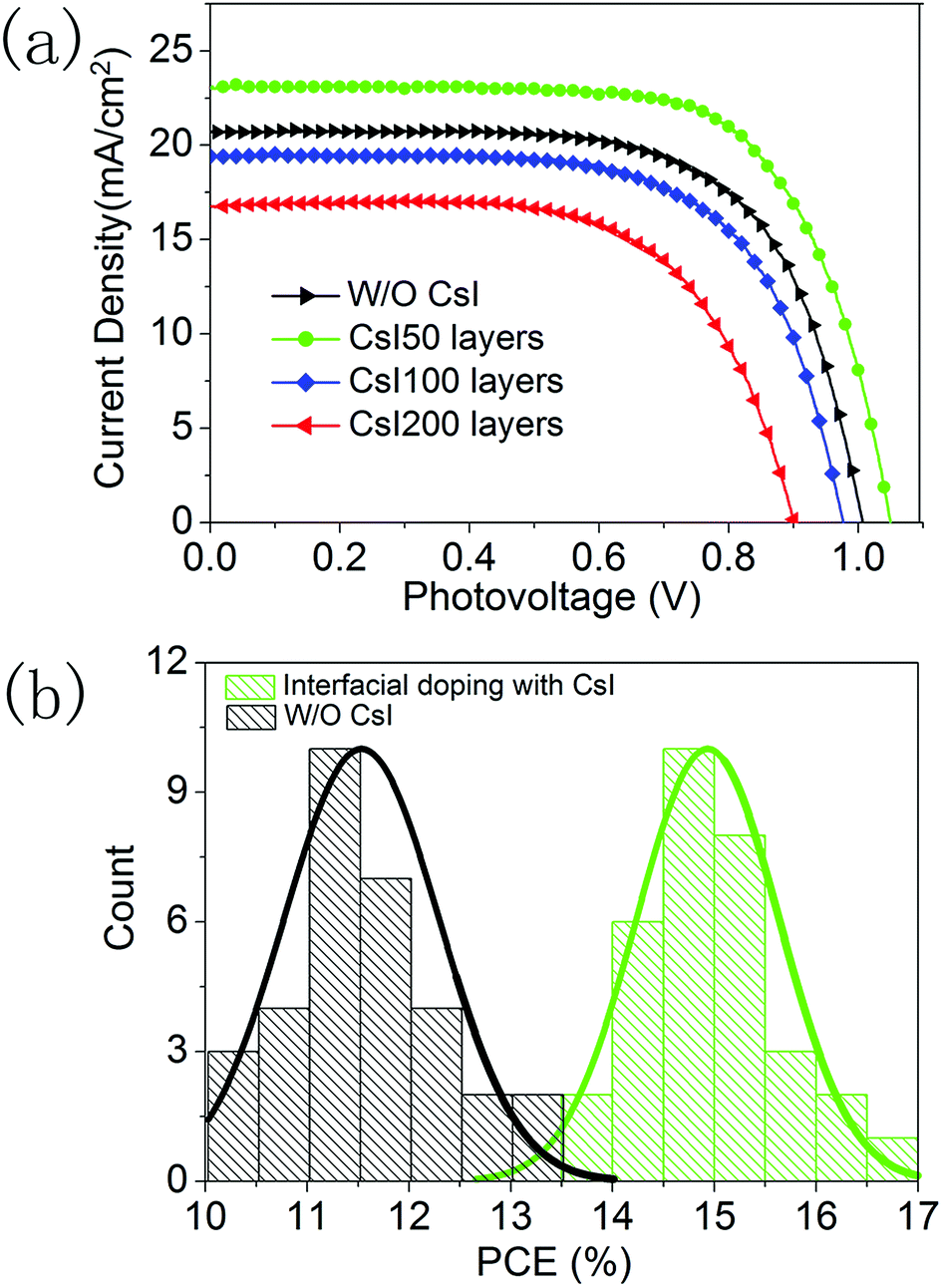 | ||
| Fig. 5 (a) J–V curves of devices without and with different CsI doping layers under one Sun illumination, and (b) statistical analysis of PCEs for 32 devices without and with CsI50 doping layers under one Sun illumination. | ||
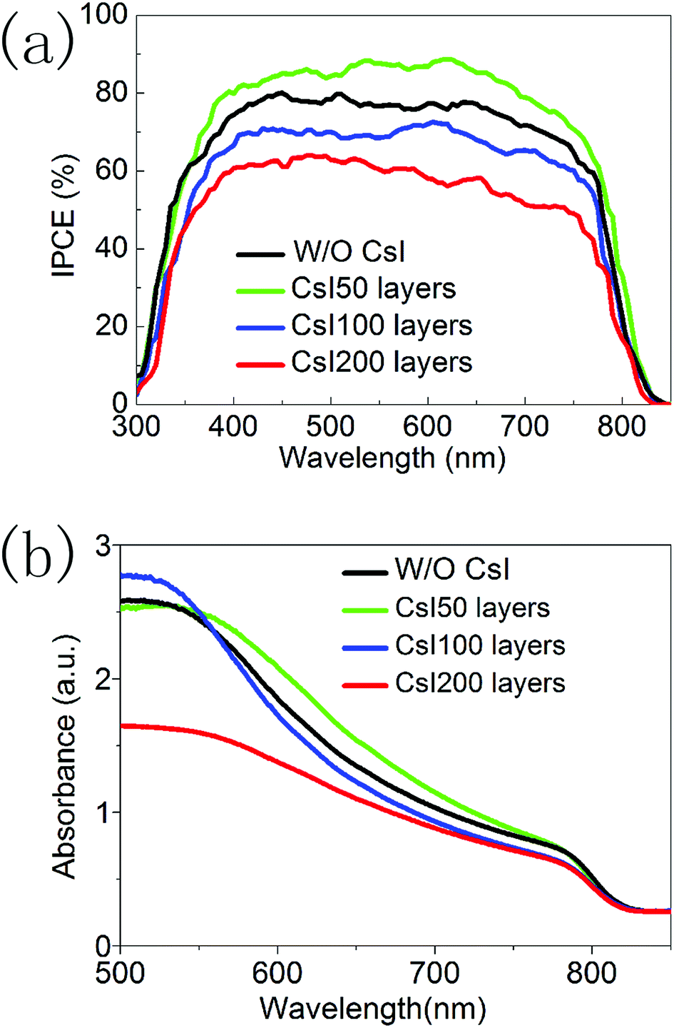
Fig. 6a shows the incident photon-to-electron conversion efficiency (IPCE) spectra of devices with different CsI doping layers. Although Cs+ ions have usually increased the bandgap of FAPbI3 in previous reports, these CsI doping layers do not lead to the blue shift in the onset wavelength (at about 840 nm). This means that these CsxFA1−xPbI3 layers prepared using the interfacial doping method are different from the ones prepared using mixed solution doping, and interfacial doping is beneficial to preserve the broad light response range of FAPbI3. In Fig. 6a, the difference of these IPCE spectra mainly comes from the IPCE values. CsI50 doping layers can lead to the increase in IPCE values, while further increasing of the CsI quantity results in the decrease of IPCE values. As IPCE spectra are directly related with the Jsc of solar cells, the tendency of IPCE values is in accordance with that of Jsc in Fig. 5a. The photovoltaic performance and IPCE spectra of these devices can be further analysed by the light absorption process and the recombination-transport process.
 | ||
| Fig. 6 (a) IPCE spectra of devices without and with different CsI doping layers. (b) Absorption spectra of perovskite layers without and with different CsI doping layers. | ||
Fig. 6b shows the light absorption spectra of perovskite layers with different CsI doping layers. All of these samples have similar absorption edges at about 840 nm. In the interfacial doping process, Cs+ ions tend to locate in the vicinity of doping interfaces, and undoped capping layers of pure FAPbI3 exist at the outer surface. Thus the light absorption range of CsxFA1−xPbI3 layers can be preserved. It is noted that CsI50 doping layers lead to an increase in the absorption coefficient in a wavelength range of 550–750 nm. However, further increasing the quantity of CsI dopant results in a decrease in absorption. This tendency is similar to the absorption of CsxFA1−xPbI3 layers prepared using the mixed solution method.16,17 The improvement of light absorption can increase the generation of photoelectrons in the conduction band of perovskite layers, and this is beneficial for the output of photocurrent.
To investigate the recombination-transport process, we performed impedance measurements for these four devices with different CsI doping layers. The Nyquist plots are shown in Fig. 7a, and they can be distinguished into two impedance arcs. The impedance arc at the low frequency comes from the recombination process in perovskite solar cells, and the impedance arc at the high frequency is usually related to the charge transfer process at interfaces.36,37 After fitting the impedance spectra with the equivalent circuit (Fig. S2†), the recombination resistance and charge transfer resistance can be extracted. Fig. 7b shows the recombination resistance of devices with different CsI doping layers under a series of applied potentials. At small applied potentials, the recombination resistance can be increased by inserting CsI50 doping layers, and this reflects the decrease in recombination velocity. It is likely related to the improvement in crystallization by inserting CsI50 doping layers. A low recombination velocity is beneficial for the transport process of photo-generated electrons, which is in accordance with the trend of the photocurrent in Fig. 5a. Further increasing the quantity of the CsI dopant (CsI100 and CsI200) leads to the decrease in the recombination resistance continuously. By increasing the bias potential, the recombination resistance decreases continuously, but its trend does not change. At high applied potentials, the relatively large recombination resistance leads to a high density of electrons in conduction bands, which is beneficial for promoting Voc of devices. Fig. 7c shows the charge transfer resistances at different applied potentials. The charge transfer resistance decreases when inserting CsI50 doping layers, but it increases after further increasing the quantity of the CsI dopant (CsI100 and CsI200). A low charge transfer resistance enhances the electron transfer at the TiO2/perovskite interfaces, which is beneficial for the charge collection process.
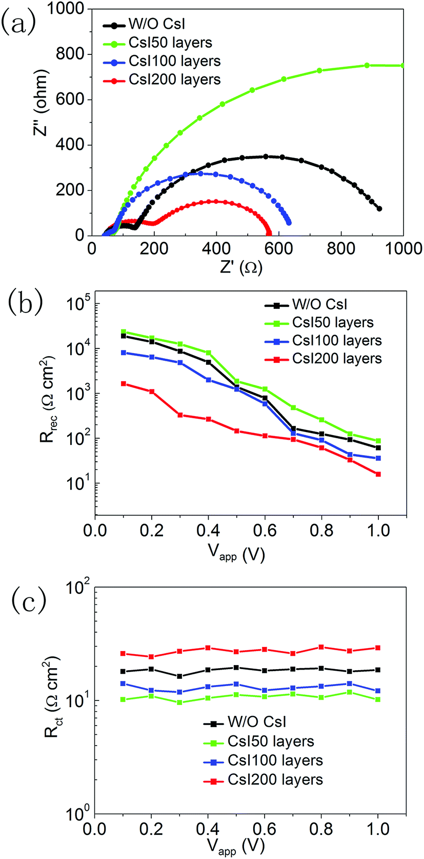 | ||
| Fig. 7 (a) Nyquist plots of devices without and with different CsI doping layers at a bias potential of 0.8 V, (b) the recombination resistance and (c) charge transfer resistance of devices under different applied potentials. | ||
We further compared the photovoltaic performance of devices prepared using the interfacial doping method and the mixed solution doping method, and 32 devices were fabricated for the statistical analysis. The CsI50 layers are used in the interfacial doping method, while 10 mol% CsI dopant is employed for the mixed solution method as in the optimization conditions of previous reports.18,19 In Fig. 8a, the best PCE of 17.1% with a Jsc of 23.0 mA cm−2, a Voc of 1.05 V and a fill-factor of 0.71 is achieved for the interfacial doping method, while the best performing device prepared using the mixed solution method gives a PCE of 15.0% with a Jsc of 21.8 mA cm−2, a Voc of 1.03 V and a fill-factor of 0.67. As shown in Fig. 4a and Fig. S1,† both doping methods can produce CsxFA1−xPbI3 layers with pure α-phase structures. However, the cutoff wavelength of IPCE spectra is 840 nm for the device prepared using the interfacial doping method, while it is 825 nm for the device prepared using the mixed solution doping method (Fig. S3†). The relatively broad wavelength range of light responses can be related to the avoidance of the blue shift for the absorption edge of the material prepared using the interfacial doping method. It is beneficial for the utilization of solar illumination, which can lead to the relatively high photocurrent density of the material prepared using the interfacial doping method. Fig. S4† shows the surface morphology of these CsxFA1−xPbI3 layers prepared using two different doping methods. The interfacial doping method leads to an average grain size of 420 nm, while the mixed solution method gives an average grain size of 330 nm. As a large size of perovskite grains reduces the scattering of charge carriers at the grain boundaries, the charge collection process can be improved by the interfacial doping method. Fig. 8b is the statistical analysis of PCEs for 32 devices prepared using these two kinds of doping methods. The devices based on interfacial doping and mixed solution doping achieve average PCEs of 14.9% and 13.4% respectively, which confirms the advantages of the interfacial doping method for CsxFA1−xPbI3 solar cells.
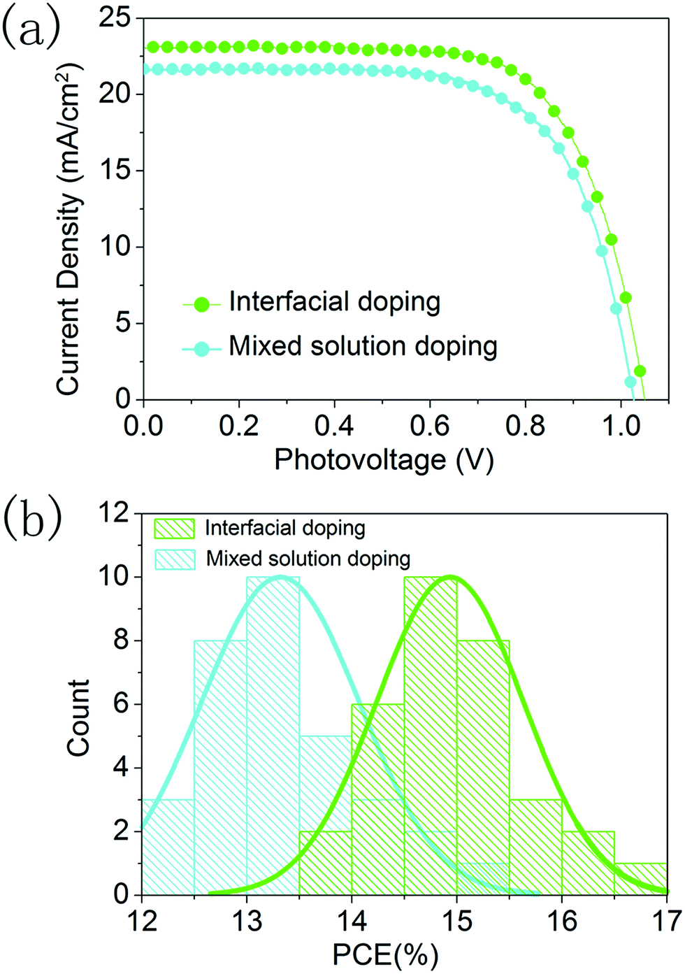 | ||
| Fig. 8 (a) J–V curves of devices prepared using mixed solution doping and interfacial doping under one sun illumination, and (b) statistical analysis of PCEs for 32 devices prepared using mixed solution doping and interfacial doping under one sun illumination. | ||
Conclusions
In summary, we developed an interfacial doping method for producing Cs+ doped FAPbI3 layers as the light harvester of perovskite solar cells. In contrast to the previous mixed solution method, the concentration of cesium dopants is very low at the outer surfaces of perovskite layers, and the majority of cesium dopants should be located in the vicinity of TiO2/perovskite interfaces. It is found that CsI doping layers affect the morphology of PbI2 layers, which subsequently improves the crystallization and morphology of CsxFA1−xPbI3 layers. For the optimized CsI doping layers, the light absorption process and charge collection process can be improved, and the PCE of devices can be increased from 13.4% to 17.1%. Light absorption spectra show that the interfacial doping method can avoid the blue shift of the absorption edge, and this is beneficial for the utilization of solar energy. Furthermore, the interfacial doping method leads to a better performance than the previous mixed solution method for CsxFA1−xPbI3 solar cells.Conflicts of interest
There are no conflicts to declare.Acknowledgements
This work was partially supported by the National Natural Science Foundation of China (Grant No. 51772125, 51273079 and 11674404) and the Jilin Provincial Research Foundation for Basic Research (Grant No. 20180101214JC).Notes and references
- A. Kojima, K. Teshima, Y. Shirai and T. Miyasaka, J. Am. Chem. Soc., 2009, 131, 6050–6051 CrossRef PubMed.
- J. Im, C. Lee, J. Lee, S. Park and N. Park, Nanoscale, 2011, 3, 4088–4093 RSC.
- H. Kim, C. Lee, J. Im, K. Lee, T. Moehl, A. Marchioro, S. Moon, R. Humphry-Baker, J. Yum, J. Moser, M. Grätzel and N. Park, Sci. Rep., 2012, 2, 591 CrossRef PubMed.
- M. Lee, J. Teushcer, T. Miyasaka, T. Murakami and H. Snaith, Science, 2012, 338, 643–647 CrossRef PubMed.
- C. Stoumpos, C. Malliakas and M. Kanatzidis, Inorg. Chem., 2013, 52, 9019–9038 CrossRef PubMed.
- W. Zhang, G. Eperon and H. Snaith, Nat. Energy, 2016, 1, 16048 CrossRef.
- W. Yang, J. Noh, N. Jeon, Y. Kim, S. Ryu, J. Seo and S. Seok, Science, 2015, 348, 1234–1237 CrossRef PubMed.
- G. Eperon, S. Stranks, C. Menelaou, M. Johnston, L. Herz and H. Snaith, Energy Environ. Sci., 2014, 7, 982–988 RSC.
- W. Yang, B. Park, E. Jung, N. Jeon, Y. Kim, D. Lee, S. Shin, J. Seo, E. Kim, J. Noh and S. Seok, Science, 2017, 356, 1376–1379 CrossRef PubMed.
- S. Pang, H. Hu, J. Zhang, S. Lv, Y. Yu, F. Wei, T. Qin, H. Xu, Z. Liu and G. Cui, Chem. Mater., 2014, 26, 1485–1491 CrossRef.
- M. Saliba, T. Matsui, K. Domanski, J. Seo, A. Ummadisingu, S. Zakeeruddin, J. Baena, W. Tress, A. Abate, A. Hagfeldt and M. Grätzel, Science, 2016, 354, 206–209 CrossRef PubMed.
- J. Liu, Y. Shirai, X. Yang, Y. Yue, W. Chen, Y. Wu, A. Islam and L. Han, Adv. Mater., 2015, 27, 4918–4923 CrossRef PubMed.
- N. Pellet, P. Gao, G. Gregori, T. Yang, M. Nazeeruddin, J. Maier and M. Grätzel, Angew. Chem., Int. Ed., 2014, 53, 3151–3157 CrossRef PubMed.
- N. Jeon, J. Noh, W. Yang, Y. Kim, S. Ryu, J. Seo and S. Seok, Nature, 2015, 517, 476–480 CrossRef PubMed.
- J. Wu, X. Xu, Y. Zhao, J. Shi, Y. Xu, Y. Luo, D. Li, H. Wu and Q. Meng, ACS Appl. Mater. Interfaces, 2017, 9, 26937–26947 CrossRef PubMed.
- J. Lee, D. Kim, H. Kim, S. Seo, S. Cho and N. Park, Adv. Energy Mater., 2015, 5, 1501310 CrossRef.
- X. Xia, W. Wu, H. Li, B. Zheng, Y. Xue, J. Xu, D. Zhang, C. Gao and X. Liu, RSC Adv., 2016, 6, 14792–14798 RSC.
- T. Liu, Y. Zong, Y. Zhou, M. Yang, Z. Li, O. Game, K. Zhu, R. Zhu, Q. Gong and N. Padture, Chem. Mater., 2017, 29, 3246–3250 CrossRef.
- N. Zhou, Y. Shen, Y. Zhang, Z. Xu, G. Zheng, L. Li, Q. Chen and H. Zhou, Small, 2017, 13, 1700484 CrossRef PubMed.
- Y. Yu, C. Wang, C. Grice, N. Shrestha, J. Chen, D. Zhao, W. Liao, A. Cimaroli, P. Roland, R. Ellingson and Y. Yan, ChemSusChem, 2016, 9, 3288–3297 CrossRef PubMed.
- X. Zhang, G. Ji, D. Xiong, Z. Su, B. Zhao, K. Shen, Y. Yang and X. Gao, RSC Adv., 2018, 8, 987–993 RSC.
- J. Lee and S. Baik, RSC Adv., 2018, 8, 1005–1013 RSC.
- J. Wi, T. Kim, J. Kim, W. Lee, D. Cho, W. Han and Y. Chung, ACS Appl. Mater. Interfaces, 2015, 7, 17425–17432 CrossRef PubMed.
- K. Torigoe and T. Ono, Enhanced diffusion of boron by oxygen precipitation in heavily boron-doped silicon, J. Appl. Phys., 2017, 121, 215103 CrossRef.
- W. Chen, Q. Luo, X. Deng, J. Zheng, C. Zhang, X. Chen and S. Huang, RSC Adv., 2017, 7, 54068–54077 RSC.
- K. Woo, Y. Kim, W. Yang, K. Kim, I. Kim, Y. Oh, J. Kim and J. Moon, Sci. Rep., 2013, 3, 3069–3076 CrossRef PubMed.
- W. Tress, K. Leo and M. Riede, Sol. Energy Mater. Sol. Cells, 2011, 95, 2981–2986 Search PubMed.
- J. Kim, H. Choi, C. Nahm, C. Kim, J. Kim, W. Lee, S. Kang, B. Lee, T. Hwang, H. Park and B. Park, Appl. Phys. Lett., 2013, 102, 183901 CrossRef.
- K. Cho, S. Paek, G. Grancini, C. Carmona, P. Gao, Y. Lee and M. Nazeeruddin, Energy Environ. Sci., 2017, 10, 621–627 RSC.
- M. Kim, B. Kim, D. Son, N. Park, H. Jung and M. Cho, Nano Lett., 2016, 16, 5756–5763 CrossRef PubMed.
- O. Ergen, S. Gilbert, T. Pham, S. Turner, M. Tan, M. Worsley and A. Zettl, Nat. Mater., 2017, 16, 522–525 CrossRef PubMed.
- Y. Wu, A. Islam, X. Yang, C. Qin, J. Liu, K. Zhang, W. Peng and L. Han, Energy Environ. Sci., 2014, 7, 2934–2938 RSC.
- F. Shao, L. Xu, Z. Tian, Y. Xie, Y. Wang, P. Sheng, D. Wang and F. Huang, RSC Adv., 2016, 6, 42377–42381 RSC.
- R. Niemann, L. Gouda, J. Hu, S. Tirosh, R. Gottesman, P. Camerona and A. Zabanb, J. Mater. Chem. A, 2017, 4, 17819–17827 RSC.
- T. Zhang, M. Dar, G. Li, F. Xu, N. Guo, M. Grätzel and Y. Zhao, Sci. Adv., 2017, 3, 1700841 CrossRef PubMed.
- J. Zhang, E. Perez, I. Sero, B. Viana and T. Pauporte, J. Mater. Chem. A, 2015, 3, 4909–4915 RSC.
- E. Perez, M. Wuβler, F. Santiago, K. Wollny, E. Mankel, T. Mayer, W. Jaegermann and I. Sero, J. Phys. Chem. Lett., 2014, 5, 680–685 CrossRef PubMed.
Footnote |
| † Electronic supplementary information (ESI) available. See DOI: 10.1039/c8ra04742a |
| This journal is © The Royal Society of Chemistry 2018 |