
 Open Access Article
 This Open Access Article is licensed under a Creative Commons Attribution-Non Commercial 3.0 Unported Licence
Fast near infrared sintering of silver nanoparticle ink and applications for flexible hybrid circuits†
Weibing Gu ab,
Wei Yuanb,
Tao Zhongc,
Xinzhou Wub,
Chunshan Zhoub,
Jian Linb and
Zheng Cui*b
ab,
Wei Yuanb,
Tao Zhongc,
Xinzhou Wub,
Chunshan Zhoub,
Jian Linb and
Zheng Cui*b
aUniversity of Chinese Academy of Sciences, China
bPrintable Electronics Research Centre, Suzhou Institute of Nanotech and Nano-bionics, Chinese Academy of Sciences(SINANO), Suzhou, China 215123. E-mail: zcui2009@sinano.ac.cn
cCollege of Information Engineering. China Jiliang University (CJLU), Hangzhou, 310018, China
First published on 28th August 2018
Abstract
Near infrared(NIR) sintering technology is a photonic sintering approach for metal nanoparticle inks, which can selectively sinter metal nanoparticle inks more quickly and efficiently, and it is also compatible with high-throughput manufacturing processes. In this paper, silver nanoparticle (AgNP) ink sintered by near infrared light at a peak wavelength of 1100 nm was investigated. After only 8 seconds of exposure to NIR irradiation, resistivity of 2.78 μΩ cm was achieved for thin films printed with AgNP ink, which was only 1.7-fold higher than that of bulk silver (1.59 μΩ cm). The structure of the sintered silver film was examined by sintering printed silver nanoparticle ink samples having different thicknesses, and the results showed that AgNPs were homogeneously coalesced throughout the cross-sections of films, indicating the formation of dense silver layers. Furthermore, the morphology and electrical resistivity of the sintered AgNP film dried by NIR were compared with those of the film dried on a hot plate. It was found that drying conditions with a relatively long drying time rather than the drying temperature contributed to the reduction of voids in the film and to the improvement in its density and electrical performance. Finally, a flexible hybrid circuit integrated with a microcontroller chip on a poly(ethylene terephthalate)(PET) substrate was fabricated by screen printing with AgNP ink for interconnects, and its surface roughness and flexibility were investigated.
Introduction
Printed electronics have attracted a lot of attention, and they have been investigated intensively over the past decade.1–5 In contrast to traditional electronic device fabrication processes, which require vacuum deposition, photolithography and etch steps, the method for printed electronics is an additive method, which only needs a two-step process to fabricate electronic devices and circuits.6 In general, various printing technologies such as screen,7 inkjet,8 gravure,9 flexography,10 and offset11 can be used to directly deposit functional materials in patterns; the materials are used more efficiently with less waste, which is especially beneficial for large-area electronic systems using expensive materials. Furthermore, printing is compatible with flexible substrates such as polymer foils and papers and can produce flexible electronic devices under ambient conditions. The advantages of faster, simpler and cheaper processes compared to those of conventional techniques contribute to the commercial success of printed or flexible electronic devices. Recently, many novel applications have been demonstrated such as printed thin film transistors,12 photovoltaic devices,13 sensors,14 displays,15 radio frequency identification tags (RFID)16 and wearable electronics.17The key feature of printed electronics is the use of functional inks to fabricate components for flexible electronic devices. Many materials can be formulated into printable inks including conductors,18 semiconductors,19 and insulating materials20 as well as optical, chemical, magnetic or biological materials.21,22 So far, conductive ink is one of the most widely researched subjects in printed electronics due to its wide use in almost every printed electronic device. A broad class of materials including conductive polymers23 and metal-based24 and carbon-based25 materials has been studied for the formulation of conductive inks. In particular, conductive inks prepared with metallic nanoparticles are mostly employed because of their high conductivity and low melting point. Kamyshny and Magdassi26 reviewed conductive inks based on metallic nanoparticles, carbon nanotubes, and graphene and discussed their applications for printed electronics. Currently, gold (Au), silver (Ag), and copper (Cu) nanoparticles are commonly used for printing conductive elements due to their superior electrical conductivities.27 Among them, Ag is often chosen because it exhibits stability against oxidation in air compared to copper, and it is also less expensive than gold. Although Cu has much lower cost as a raw material than Ag, it is easily oxidized to copper oxide in post processing, creating a barrier to electron conduction.28 To well disperse the metallic nanoparticles in a desired solvent and to achieve high material loading, stabilizing polymers are employed to prevent nanoparticle aggregation. Polymers (polyacrylic acid (PAA)29 or polyvinylpyrrolidone (PVP)30) or some low molar mass compounds31 are frequently used as stabilizers, which can adhere to the surface of nanoparticles and repulse the dispersed metal particles with steric, electrostatic, or electrosteric effects.32
After solution deposition or printing, metallic nano-inks require drying and sintering steps to form an electronic percolation path and to improve their conductivity. In general, heat treatment is used to decompose the organic stabilizer and coalesce the nanoparticles.33 Typical heating temperatures reported in the literature range between 125 °C and 250 °C, and they are applied for up to 60 min. However, such high temperature treatment for long time is inefficient and in particular unsuitable for polymer-based substrates, which are commonly used in printed electronics. Hence, the development of alternative faster drying and sintering technologies with selective heating without damaging the substrate is highly desirable. Many researchers have studied various low-temperature sintering methods such as chemical,34 laser,35 spark plasma,36 electrical,37 infrared,38 microwave,39 and intense pulsed light40 methods. These techniques can successfully convert metal precursor inks (including metal organic compounds, metal salts, and metal nanoparticles) into conductive structures.
Currently, attention is being focused on developing sintering processes that are compatible with large area and high-throughput manufacturing of flexible electronics for commercialized applications. Among the aforementioned sintering techniques, infrared and intense pulsed light irradiations are most suitable for large area sintering, and they are compatible with roll-to-roll production because the sintering process occurs in a few seconds or even in a fraction of a second.27 Tobjork et al.41 demonstrated infrared sintering of AgNP ink on a paper substrate to obtain conductivity of 10–20% of that of bulk silver within 15 seconds. Cherrington et al.42 showed a more selective sintering approach by NIR irradiation to cure AgNP ink in only two seconds. Due to low NIR absorption of the polymer foil in the NIR region, the Ag nano ink was selectively heated without substrate deformation. Recently, Sowade et al.43 reported IR drying and sintering of inkjet-printed silver layers on a polyethylene naphthalate (PEN) substrate in a roll-to-roll (R2R) process. Park et al.44,45 presented NIR sintering of an R2R gravure-printed Ag layer. Hwang et al.46 developed a photonic sintering method involving intense pulsed light, NIR light and deep UV light to produce a copper film. As a fast drying and selective sintering technique, NIR has showed many potential applications in printed electronics. However, the mechanistic properties of NIR sintering have not been studied deeply. The method for sintering a nanoparticle ink into a functional film with dense microstructure and smooth surface is a target of printed electronics, which is not well-reported in previous literature. These properties will determine the performance of a sintered functional film and the range of applications in printed devices.
In this paper, fast sintering of an AgNP ink by NIR irradiation was demonstrated. The nanoparticles coalesced and formed conductive paths with low resistivity in only a few seconds. The sintering depth was investigated with AgNP films having different thicknesses, and the changes in the film microstructures were observed from the cross-sections of sintered layers by scanning electron microscopy (SEM). The effects of drying conditions on electrical performance and morphology were compared for both NIR and hot plate drying processes. The surface roughness under different drying and sintering conditions was measured. Furthermore, a flexible hybrid circuit integrated with silicon chips was fabricated by screen printing and sintered with NIR on PET substrates. The mechanical stability of the printed flexible circuit in terms of adhesion to the flexible substrate was also evaluated.
Experimental
Specimen preparation
The silver nanoparticle ink was purchased from PARU Company (PG-007, Screen printing ink), and it contained 80 wt% AgNP dispersed in glycols. The sizes of silver particles were in the range of 20–200 nm, with most of the NPs falling in the 50–150 nm range. To study the drying and sintering effect of NIR irradiation, the ink was deposited on glass by spin coating and was compared with that dried on a hot plate (50 °C) for 10 min. To examine the sintering depth of NIR, the cross sectional areas of the samples at various thicknesses were observed, and they were scored using a diamond pen and gently broken. A flexible hybrid circuit was prepared using screen printing on a PET substrate (A4100, TOYOBO Co., Ltd.) and integrated with a micro controller chip (STM8S, STMicroelectronics).Sintering and printing apparatus
The AgNP ink was sintered by NIR irradiation at room temperature and ambient conditions. The NIR system consisting of 9 twin tube NIR lamps, a power controller and a water-cooling module (Heraeus Noblelight Co., Ltd.) had a peak wavelength at around 1100 nm. The sintering area was 300 mm × 200 mm. The maximum electrical power density of the system was 360 kW m−2. In this study, a minimum sintering time of 2 seconds was set up because a stable time was needed for NIR light irradiation. AgNP films were placed at a distance of 3.5 cm from the lamps. The output energy and on-time were adjusted to change the sintering conditions.A screen printing kit was purchased from Atma (AT-25PA, China), and it consisted of a screen mask and squeegee. The mask as an image carrier was composed of an aluminium frame and screen metal stencil. A design layout of hybrid circuit was transferred to the screen stencil.
Characterization
The morphology and cross section of the AgNP film were observed by scanning electron microscopy (SEM, Hitachi S-4800). The surface profile and thickness of the sintered film were measured with a profiler meter (Dektak XT, Bruker). A UV-visible spectrometer (Lambda 750, PerkinElmer) was used to characterize the reflectance of the AgNP film. A four-point probe station (Suzhou Jingge Electronic Co., Ltd.) was used to measure the sheet resistance at room temperature. The resistivity was calculated from the definition Rs = ρ/d, where ρ is the resistivity, Rs is the sheet resistance, and d is the thickness. The mechanical reliability of the sintered AgNP film was investigated under repeated rolling by a homemade bending tester with rolling diameter of 7 mm.Results and discussion
Fast, efficient and large-area sintering technologies are highly desirable for the fabrication of printed electrically conductive patterns. NIR irradiation enables fast heating of nanoparticles in the printable ink and reduces the sintering time to a few seconds. Fig. 1 shows the variation of electrical resistivity of silver nanoparticles sintered by NIR with power of 360 kW m−2 over 10 seconds together with cross-sectional SEM images (inset) of the sintered layer at different sintering times. The resistivity decreased tremendously in the first 4 seconds and then declined gradually as the NIR irradiation time was prolonged to 10 seconds. It can be observed from the SEM images that the polymer surrounding the silver nanoparticles was quickly eliminated in 4 seconds, as shown in Fig. 1a–c. Subsequently, the nanoparticles coalesced and sintered into a film, which formed a percolation path, resulting in improvement in electrical conductivity. The sintering process, according to the literature,47 is classified into two primary processes. First, the polymer stabilizer, which acts as a spacer and keeps the particles apart in the ink, desorbs or detaches from the metal particle surface. The metal particles then move, approach each other and get into direct contact. Second, unprotected adjacent metal particles begin to aggregate and form necks driven by surface atom diffusion, which minimizes the surface area. As the temperature of AgNPs irradiated by NIR increased quickly, the silver nanoparticles diffused with each other and formed a denser film from 6 seconds to 10 seconds (Fig. 1d–f). The NIR irradiation raised the temperature to about 700 °C in 4 seconds, as shown in Fig. S1 (ESI†). Such a high temperature contributed to stabilizer evaporation from the film and condensed the nanoparticles.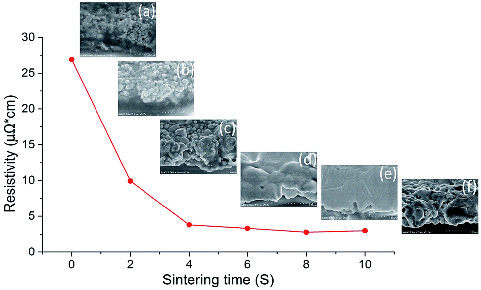 | ||
| Fig. 1 The resistivity of AgNP film sintered by NIR with power of 360 kW m−2 over 10 seconds and SEM images of the sintered film at (a) 0 second, (b) 2 seconds, (c) 4 seconds, (d) 6 seconds, (e) 8 seconds, and (f) 10 seconds. | ||
The resistivity changes in 2 second intervals during NIR sintering are summarised in Table 1. The lowest resistivity value of 2.78 μΩ cm was achieved in 8 seconds of NIR sintering, which was 1.7-fold higher than that of bulk silver (1.59 μΩ cm). To the best of our knowledge, this is the lowest resistivity ever achieved by sintering AgNP ink in seconds. It was evident from the SEM images that the film sintered in 8 seconds exhibited the densest structure (Fig. 1e), which is almost an ideal sintering state for printed AgNP ink. Generally, a higher sintering energy or temperature tends to decrease the resistivity further (ESI Fig. S2†), which is consistent with the previously reported results.48 However, when the sintering time approached 10 seconds in our case, the resistivity slightly increased due to the formation of small voids in the film.
| Sintering time (S) | 0 | 2 | 4 | 6 | 8 | 10 |
|---|---|---|---|---|---|---|
| Resistivity (μΩ cm) | 26.9 | 9.92 | 3.8 | 3.32 | 2.78 | 2.99 |
It is noteworthy that huge morphology change also occurred in the film shown in Fig. 1f due to these microscopic voids, which was caused by high sintering temperature. As shown in Fig. S1 (ESI†), due to NIR irradiation, the temperature continued to rise and reached about 1000 °C when the sintering time was prolonged from 8 seconds to 10 seconds. In the AgNP film, there are two factors or sources that lead to the increase in voids. One is the small gaps between the sintered nanoparticles in Fig. 1e, which expanded at such a high temperature for a longer time, resulting in the formation of more voids; another is that a small amount of polymer that remained in the film evaporated and was eliminated from the film, thus creating voids. Meanwhile, the surface roughness of the sintered film was slightly higher than that shown in Fig. 1e due to the formation of a porous structure.
For printed conductive films using a nanoparticle ink, sintering the nanoparticles into a dense structure with high conductivity is desired, and the microstructure of the sintered film is essential for the electrical performance. From the SEM images of Fig. 1, it can be observed that the nanoparticles homogeneously coalesced and diffused to form a dense film during the sintering process. No differences in the sintering states between the bottom side and top side near the film surface were found. Also, no swelling or peeling appeared in the film, which often occurs in fast sintering techniques such as flash lamp sintering because of shallow sintering depth.49 To examine the sintering depth of NIR, AgNP films having various thicknesses from 1.7 μm to 7.8 μm were prepared and carefully checked during the sintering process; this covered the deposition thickness range of most printing methods. Fig. 2 shows cross sectional images of the sintered film in the states of polymer detachment or decomposition and neck formation. In this stage, the nanoparticles that had absorbed NIR energy coalesced, and necks grew rapidly after the stabilizer evaporated. If the absorption of NIR irradiation across the film thickness is non-uniform, the differences of sintering states can be clearly presented.50 Fortunately, as NIR light can partially penetrate into the nanoparticle film,51 the silver particles inside the film were also sintered by NIR absorption. Even for thick films, as shown in Fig. 2e, the nanoparticles on the bottom exhibited the same sintering state as that on the top side, which indicated that the depth of NIR absorption is greater than 7.8 μm. In addition, it is noteworthy that the sintering of AgNP film was a negative feedback process, i.e., the reflectance to NIR irradiation increased when the nanoparticles were sintered to coalesce and become a conductive film (ESI Fig. S3†). Such effect also contributed to the uniformity of nanoparticle sintering.
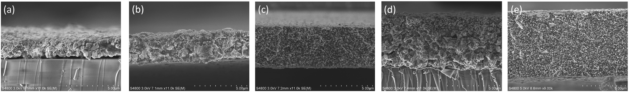 | ||
| Fig. 2 Cross section images of the NIR-sintered AgNP film with thicknesses of (a) 1.7 μm; (b) 3.1 μm; (c) 4.2 μm; (d) 5.4 μm; (e) 7.8 μm. | ||
For printed electronic applications, it would be advantageous if both drying and sintering of the printed ink can use the same technology, which can simplify the process, reduce the processing time, and enable roll-to-roll manufacturing. Therefore, NIR was investigated for both drying and sintering of the AgNP film. In particular, the drying condition was evaluated for its influence on electrical performance. Fig. 3 shows the microstructure of the AgNP film sintered by NIR but with different drying conditions. The films, as shown in Fig. 3b and c, were dried by NIR with 72 kW m−2 for 50 seconds and 108 kW m−2 for 20 seconds, respectively. Interestingly, it can be found that relatively larger voids were present in the film with higher drying temperatures (Fig. 3c). A denser film with smaller voids was achieved with a relatively longer drying time (Fig. 3b) although the drying temperature was lower than that in Fig. 3c. It seems that prolonging the drying time rather than raising the drying temperature contributed to reducing the voids in the sintered film. To confirm this point, a drying process with a hot plate at 50 °C for 10 minutes was conducted, and the densest film was obtained with few voids (Fig. 3a). In contrast, the AgNP film sintered by NIR directly, which could also be considered to be drying and sintering under combined conditions, showed more voids in the film (Fig. 3d). The possible reason for this phenomenon can be due to the degree of solvent or polymer evaporation. With longer drying times, more solvent or polymer evaporated, allowing nanoparticles to approach each other more closely; hence, fewer voids occurred and a denser film was formed in the subsequent sintering process. It should be noted that peeling of the film may happen if it is directly sintered with NIR without the prior drying step (Fig. S4, ESI†). This was due to the amount of gas released, which was more severe if significant amounts of polymers or organic compounds remained in the film.
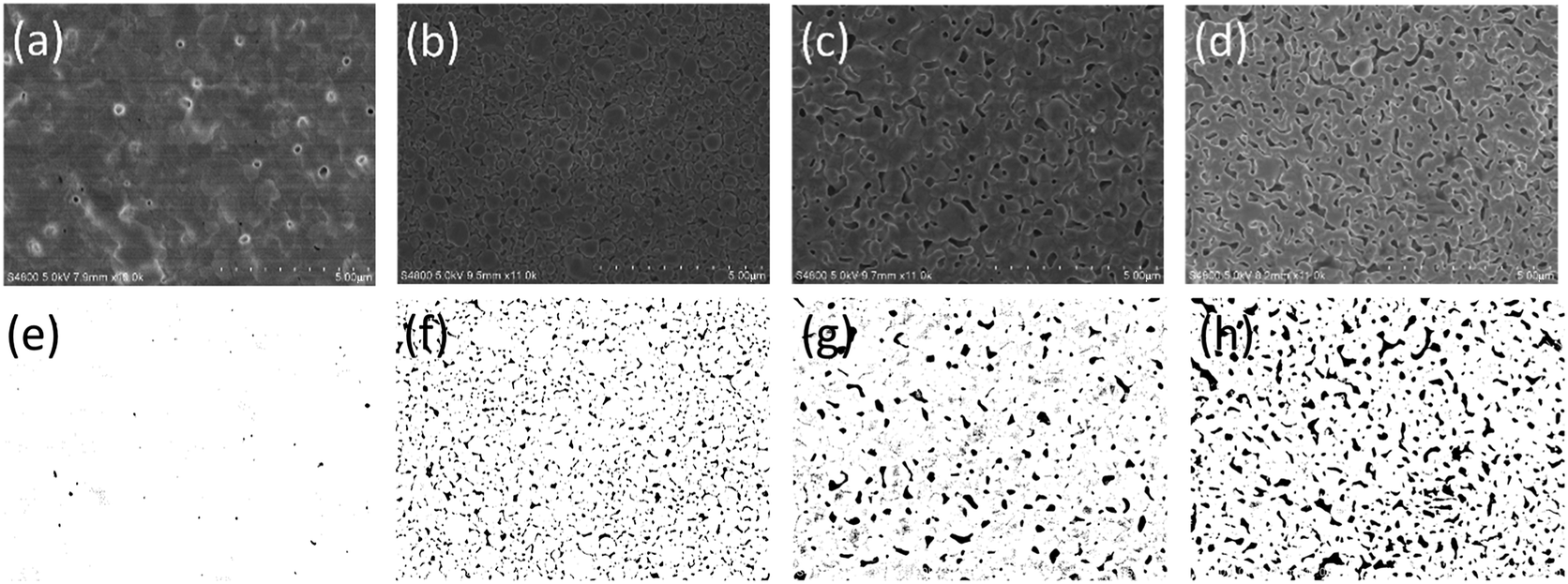 | ||
| Fig. 3 Microstructure images of sintered AgNP film with different drying methods and the corresponding images processed using MATLAB: (a) dried by hot plate at 50 °C for 10 min and (e) the processed image, (b) dried by NIR with 72 kW m−2 for 50 s and (f) the processed image, (c) dried by NIR with 108 kW m−2 for 20 s and (g) the processed image, (d) sintered by NIR directly and (h) the processed image. | ||
The resistivity values of the sintered AgNP film with different drying methods are listed in Table 2. It can be seen that the resistivity increased as the drying time reduced and the voids increased. To evaluate the effect of voids on resistivity, MATLAB was used to process the SEM images of Fig. 3a–d, and the void percentage was computed after applying an appropriate threshold (Fig. 3e–h). For image processing, black areas were treated as voids and white areas as silver. The void percentage values are summarised in Table 2. The data show that the variation of void percentage is in accordance with the change in resistivity. The film with void percentage of 6.5% corresponds to resistivity of 5 μΩ cm. When the void percentage is increased to 7.4% by drying with NIR at 108 kW m−2 for 20 seconds, the resistivity is also slightly increased to 5.1 μΩ cm. Furthermore, as the void percentage increases to 13.3%, the resistivity increases to 6.5 μΩ cm. In contrast, the film with void percentage of 0.12% has the lowest resistivity.
| Method of drying | Hot plate 50 °C 10 min | NIR 72 kW m−2 50 s | NIR 108 kW m−2 20 s | Non |
|---|---|---|---|---|
| Resistivity (μΩ cm) | 2.78 | 5 | 5.1 | 6.5 |
| Void percentage (%) | 0.12 | 6.5 | 7.4 | 13.3 |
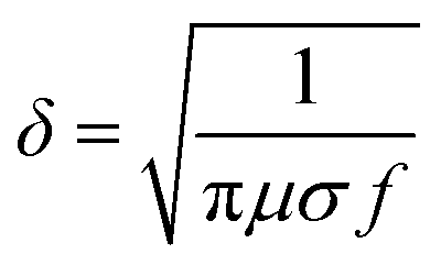
Besides resistivity, surface roughness of printed conductive patterns would also influence the quality of signal transmission, especially when the patterns act as conductive lines or RF antennas in high-frequency circuit systems. This is because the skin effect would stand out during current transfer, which is defined that the electric current distributed within a conductor that is mainly at the “skin” of the conductor. This means that the current density is the largest near the surface of the conductor and decreases with depths in the conductor. The skin depth (δ) is calculated by using the general formula,
In general, the surface roughness of a printed film is larger than that formed by vacuum deposition, which can lead to impedance changes and signal loss. To achieve reliable high frequency signal transmission, surface roughness less than 1 μm is expected for actual applications of printed conductive circuits in flexible high-frequency electrics. As mentioned before, sintering techniques and conditions have great influence on the morphology of printed nanoparticle films. Fig. 4 shows the surface profile of sintered AgNP film with NIR and hot plate, which underwent a drying process before sintering. It can be observed that the roughness increased with increasing NIR sintering times. The roughness reached about 0.6 μm when the nanoparticles were fully sintered with NIR for 10 seconds, which was about 3 times of that obtained by sintering with a hot plate for 15 minutes. This is due to rapid elimination of polymer or organics from the printed film with fast NIR sintering. Predictably, the AgNP film sintered by NIR directly (in Fig. 3d), which resulted in intense evaporation of the polymer and numerous void formations in the film, exhibited the largest roughness (ESI Fig. S5†). However, the roughness of NIR-sintered films (Fig. 4) was less than 1 μm, and the conductive patterns meet the demands of applications in high-frequency circuits.
 | ||
| Fig. 4 The surface profile of sintered AgNP film with hot plate at 120 °C and NIR with power of 360 kW m−2. | ||
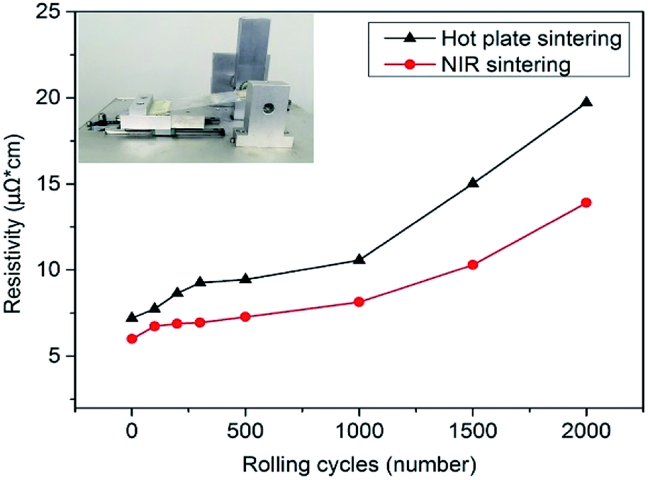
Flexibility in terms of bending stability is also an important property for flexible electronic applications. To examine the flexibility of NIR-sintered AgNP films, flexible conductive patterns were prepared on a PET substrate of 125 μm thickness, and bending tests were performed by repeated rolling with roller diameter of 7 mm (inset figures in Fig. 5). The resistivity variation after bending is shown in Fig. 5. With an increase in rolling cycles, the resistivity increased gradually. After rolling 2000 times, the resistivity of the conductive patterns sintered with NIR rose to 13.9 μΩ cm, which was ∼2 times higher than that before rolling. In comparison, the resistivity of the AgNP film sintered by a hot plate was ∼3 times higher than the initial value. The difference in resistivity change was because of their respective sintering mechanisms. For hot plate baking, a long processing time is required, and the temperature cannot exceed 150 °C as a higher temperature can result in PET deformation. Furthermore, the temperature is transmitted from the PET substrate to nanoparticles in this manner. While sintering by NIR, the applied irradiation leads to a temperature rise of the nanoparticles directly. As the PET substrate has negligible absorption in the NIR range (ESI Fig. S6†) and the sintering time is short to a few seconds, much energy can be exerted, and the temperature of the nanoparticles raised by NIR irradiation is more than 150 °C, which results in a better coalescence or sintering degree than that for hot plate baking. Furthermore, unlike hot plate baking, NIR was irradiated from the AgNP film side, and the heat was transmitted from nanoparticles to the PET substrate, which contributed to the nanoparticles fusing into the polymer substrate locally and increased adhesion.53 As the NIR sintering time is short, the PET substrate was not damaged by the transmitted heat on the macroscale. On the other hand, the larger change in resistivity with hot plate sintering was due to the decreasing contact between adjacent particles, which were incompletely sintered, and some microcracks appeared after rolling (ESI Fig. S7†).
 | ||
| Fig. 5 Bending test results of AgNP patterns sintered with NIR and hot plate (inset: photo of homemade bending tester). | ||
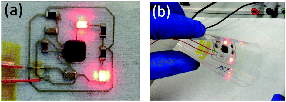
To demonstrate the suitability of NIR sintering techniques for printed electronics, a flexible hybrid circuit was designed and fabricated by integrating a microcontroller chip and printed interconnects on a PET substrate. The flexible conductive circuit was screen printed and sintered with NIR irradiation. Then, the controller chip and electrical components were integrated on the flexible circuit with low-temperature thermo-compression bonding using an anisotropic conductive paste (DELO AC265). The controller chip was programmed to flash an LED (Fig. 6a). After bending and twisting the PET substrate, the hybrid circuit system could still function normally (Fig. 6b), which showed that the printed hybrid circuit had good mechanical properties.
 | ||
| Fig. 6 Flexible hybrid circuit integrated silicon chip and printed circuit in (a) working state and (b) bending state. | ||
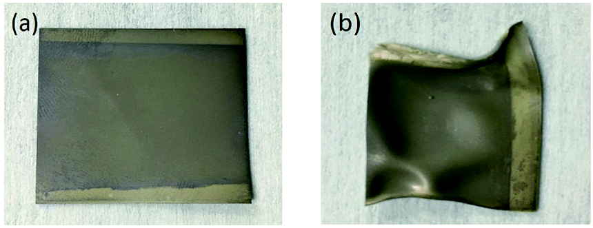
It should be noted that the results of NIR sintering in the present study are based on the nanoparticle ink. Although there is minimal absorption by PET in the NIR range (ESI, Fig. S6†), thermal effects caused by NIR can still damage the substrate after processing at a high temperature or for a long time. As shown in Fig. 7b, the flexible substrate was deformed at an irradiation power of 144 kW m−2 in 4 seconds. With higher powers or longer processing times, the deformation of the flexible substrate was more serious. However, at a power of 108 kW m−2 for 15 seconds (Fig. 7a), the PET substrate was not damaged, and resistivity of 6 μΩ cm was achieved. Fortunately, NIR irradiation enables fast heating of nanoparticles in a few seconds, and the heat transfer to the flexible substrate that leads to deformation needs some time; thus, it is possible to sinter the nanoparticle ink without damaging the PET substrate. Nonetheless, a balance should be struck between the irradiation power and processing time on the thermo-sensitive substrate. Alternatively, a high power flash of NIR followed by low-power irradiation can also achieve good sintering. For example, it was observed that when the silver ink was irradiated with a high NIR power for a few seconds followed by decrease in the sintering temperature to about 150 °C, AgNPs began to sinter together in the low-temperature stage. In this way, the silver ink could be sintered without depositing too much energy into the substrate, thus reducing the risk of plastic substrate damage. This may open a new way for sintering nanoparticle inks on flexible substrates. The mechanism of this phenomenon will be further researched and discussed in another article.
 | ||
| Fig. 7 The photos of flexible substrate with irradiation of (a) 108 kW m−2 in 15 seconds and (b) 144 kW m−2 in 4 seconds. | ||
Conclusions
This study demonstrated that AgNP-based printable inks could be sintered by NIR irradiation in a fast and efficient manner without damaging flexible substrates. A microscopically dense silver film was obtained with only 8 seconds of NIR irradiation. A resistivity value of 2.78 μΩ cm was achieved for the sintered silver film, which was only 1.7-fold higher than that of bulk silver (1.59 μΩ cm). To the best of our knowledge, this is the lowest resistivity ever achieved by sintering AgNP ink over a few seconds. Due to deep absorption of NIR, Ag nanoparticle ink with a thickness up to 8 μm could be sintered uniformly. Besides sintering parameters, drying conditions in terms of temperature and time also strongly influenced the electrical resistivity and morphology of AgNP film. The surface roughness and mechanical flexibility of the sintered film were also investigated. As a practical demonstration, a hybrid circuit on a flexible PET substrate was fabricated by printing AgNP ink to form interconnects and integrating a microcontroller chip to control the light emission of the LED. The hybrid circuit worked well even when subjected to bending and twisting.Conflicts of interest
There are no conflicts to declare.Acknowledgements
This work was supported by the Strategic Priority Research Program of the Chinese Academy of Sciences (Grant No. XDA09020201), National Program on Key Basic Research Project of China (973 Program, Grant No. 2015CB351904), and the National Natural Science Foundation of China (Grant No. 51603227).References
- P. F. Moonen, I. Yakimets and J. Huskens, Adv. Mater., 2012, 24, 5526–5541 CrossRef PubMed.
- R. Singh, E. Singh and H. S. Nalwa, RSC Adv., 2017, 7, 48597–48630 RSC.
- F. Torrisi, T. Hasan, W. P. Wu, Z. P. Sun, A. Lombardo, T. S. Kulmala, G. W. Hsieh, S. J. Jung, F. Bonaccorso, P. J. Paul, D. P. Chu and A. C. Ferrari, ACS Nano, 2012, 6, 2992–3006 CrossRef PubMed.
- M. Singh, H. M. Haverinen, P. Dhagat and G. E. Jabbour, Adv. Mater., 2010, 22, 673–685 CrossRef PubMed.
- M. Caironi, E. Gili, T. Sakanoue, X. Y. Cheng and H. Sirringhaus, ACS Nano, 2010, 4, 1451–1456 CrossRef PubMed.
- S. Hong, J. Yeo, G. Kim, D. Kim, H. Lee, J. Kwon, H. Lee, P. Lee and S. H. Ko, ACS Nano, 2013, 7, 5024–5031 CrossRef PubMed.
- O. D. Renedo, M. A. Alonso-Lomillo and M. J. A. Martinez, Talanta, 2007, 73, 202–219 CrossRef PubMed.
- S. H. Ko, H. Pan, C. P. Grigoropoulos, C. K. Luscombe, J. M. J. Frechet and D. Poulikakos, Nanotechnology, 2007, 18, 345202 CrossRef.
- E. B. Secor, S. Lim, H. Zhang, C. D. Frisbie, L. F. Francis and M. C. Hersam, Adv. Mater., 2014, 26, 4533–4538 CrossRef PubMed.
- D. Deganello, J. A. Cherry, D. T. Gethin and T. C. Claypole, Thin Solid Films, 2010, 518, 6113–6116 CrossRef.
- M. Pudas, J. Hagberg and S. Leppavuori, Prog. Org. Coat., 2004, 49, 324–335 CrossRef.
- K. H. Lee, S. M. Kim, H. Jeong, Y. Pak, H. Song, J. Park, K. H. Lim, J. H. Kim, Y. S. Kim, H. C. Ko, I. K. Kwon and G. Y. Jung, Adv. Mater., 2013, 25, 3209–3214 CrossRef PubMed.
- H. Lu, J. Lin, N. Wu, S. H. Nie, Q. Luo, C. Q. Ma and Z. Cui, Appl. Phys. Lett., 2015, 106, 4 Search PubMed.
- D. D. Liana, B. Raguse, L. Wieczorek, G. R. Baxter, K. Chuah, J. J. Gooding and E. Chow, RSC Adv., 2013, 3, 8683–8691 RSC.
- F. Villani, P. Vacca, G. Nenna, O. Valentino, G. Burrasca, T. Fasolino, C. Minarini and D. della Sala, J. Phys. Chem. C, 2009, 113, 13398–13402 CrossRef.
- J. F. Salmeron, F. Molina-Lopez, D. Briand, J. J. Ruan, A. Rivadeneyra, M. A. Carvajal, L. F. Capitan-Vallvey, N. F. Derooij and A. J. Palma, J. Electron. Mater., 2014, 43, 604–617 CrossRef.
- X. D. Wang, L. Dong, H. L. Zhang, R. M. Yu, C. F. Pan and Z. L. Wang, Adv. Sci., 2015, 2, 1500169 CrossRef PubMed.
- Z. L. Zhang, X. Y. Zhang, Z. Q. Xin, M. M. Deng, Y. Q. Wen and Y. L. Song, Nanotechnology, 2011, 22, 8 Search PubMed.
- N. Rouhi, D. Jain and P. J. Burke, ACS Nano, 2011, 5, 8471–8487 CrossRef PubMed.
- X. Ding, Y. X. Li, D. Wang and Q. R. Yin, Ceram. Int., 2004, 30, 1885–1887 CrossRef.
- C. Sekine, Y. Tsubata, T. Yamada, M. Kitano and S. Doi, Sci. Technol. Adv. Mater., 2014, 15, 15 CrossRef PubMed.
- J. Alaman, R. Alicante, J. I. Pena and C. Sanchez-Somolinos, Materials, 2016, 9, 47 CrossRef PubMed.
- S. H. Eom, H. Park, S. H. Mujawar, S. C. Yoon, S. S. Kim, S. I. Na, S. J. Kang, D. Khim, D. Y. Kim and S. H. Lee, Org. Electron., 2010, 11, 1516–1522 CrossRef.
- J. W. Chung, S. W. Ko, N. R. Bieri, C. P. Grigoropoulos and D. Poulikakos, Appl. Phys. Lett., 2004, 84, 801–803 CrossRef.
- W. W. Xu, Z. Liu, J. W. Zhao, W. Y. Xu, W. B. Gu, X. Zhang, L. Qian and Z. Cui, Nanoscale, 2014, 6, 14891–14897 RSC.
- A. Kamyshny and S. Magdassi, Small, 2014, 10, 3515–3535 CrossRef PubMed.
- S. Wunscher, R. Abbel, J. Perelaer and U. S. Schubert, J. Mater. Chem. C, 2014, 2, 10232–10261 RSC.
- D. Y. Deng, Y. X. Jin, Y. R. Cheng, T. K. Qi and F. Xiao, ACS Appl. Mater. Interfaces, 2013, 5, 3839–3846 CrossRef PubMed.
- M. Grouchko, A. Kamyshny, C. F. Mihailescu, D. F. Anghel and S. Magdassi, ACS Nano, 2011, 5, 3354–3359 CrossRef PubMed.
- K. M. Koczkur, S. Mourdikoudis, L. Polavarapu and S. E. Skrabalak, Dalton Trans., 2015, 44, 17883–17905 RSC.
- S. Mourdikoudis and L. M. Liz-Marzan, Chem. Mater., 2013, 25, 1465–1476 CrossRef.
- A. R. Studart, E. Amstad and L. J. Gauckler, Langmuir, 2007, 23, 1081–1090 CrossRef PubMed.
- E. Halonen, T. Viiru, K. Ostman, A. L. Cabezas and M. Mantysalo, IEEE Trans. Compon., Packag., Manuf. Technol., 2013, 3, 350–356 Search PubMed.
- M. Layani, M. Grouchko, S. Shemesh and S. Magdassi, J. Mater. Chem., 2012, 22, 14349–14352 RSC.
- H. Lee, S. Hong, J. Kwon, Y. D. Suh, J. Lee, H. Moon, J. Yeo and S. H. Ko, J. Mater. Chem. A, 2015, 3, 8339–8345 RSC.
- S. Wunscher, S. Stumpf, A. Teichler, O. Pabst, J. Perelaer, E. Beckert and U. S. Schubert, J. Mater. Chem., 2012, 22, 24569–24576 RSC.
- H. Andersson, A. Rusu, A. Manuilskiy, S. Haller, S. Ayoz and H. E. Nilsson, Microelectron. J., 2011, 42, 21–27 CrossRef.
- A. Denneulin, A. Blayo, C. Neuman and J. Bras, J. Nanopart. Res., 2011, 13, 3815–3823 CrossRef.
- J. Perelaer, M. Klokkenburg, C. E. Hendriks and U. S. Schubert, Adv. Mater., 2009, 21, 4830–4834 CrossRef PubMed.
- B. Y. Wang, T. H. Yoo, Y. W. Song, D. S. Lim and Y. J. Oh, ACS Appl. Mater. Interfaces, 2013, 5, 4113–4119 CrossRef PubMed.
- D. Tobjork, H. Aarnio, P. Pulkkinen, R. Bollstrom, A. Maattanen, P. Ihalainen, T. Makela, J. Peltonen, M. Toivakka, H. Tenhu and R. Osterbacka, Thin Solid Films, 2012, 520, 2949–2955 CrossRef.
- M. Cherrington, T. C. Claypole, D. Deganello, I. Mabbett, T. Watson and D. Worsley, J. Mater. Chem., 2011, 21, 7562–7564 RSC.
- E. Sowade, H. Kang, K. Y. Mitra, O. J. Weiss, J. Weber and R. R. Baumann, J. Mater. Chem. C, 2015, 3, 11815–11826 RSC.
- J. Park, H. J. Kang, K. H. Shin and H. Kang, Sci. Rep., 2016, 6, 11 CrossRef PubMed.
- J. Park, H. J. Kang, H. Gil, K. H. Shin and H. Kang, J. Mater. Chem. C, 2016, 4, 8884–8888 RSC.
- H. J. Hwang, K. H. Oh and H. S. Kim, Sci. Rep., 2016, 6, 19696 CrossRef PubMed.
- B. Ingham, T. H. Lim, C. J. Dotzler, A. Henning, M. F. Toney and R. D. Tilley, Chem. Mater., 2011, 23, 3312–3317 CrossRef.
- T. Ohlund, A. Schuppert, B. Andres, H. Andersson, S. Forsberg, W. Schmidt, H. E. Nilsson, M. Andersson, R. Y. Zhang and H. Olin, RSC Adv., 2015, 5, 64841–64849 RSC.
- D. J. Lee, S. H. Park, S. Jang, H. S. Kim, J. H. Oh and Y. W. Song, J. Micromech. Microeng., 2011, 21, 7 Search PubMed.
- S. H. Park, S. Jang, D. J. Lee, J. Oh and H. S. Kim, J. Micromech. Microeng., 2013, 23, 9 Search PubMed.
- K. Maekawa, K. Yamasaki, T. Niizeki, M. Mita, Y. Matsuba, N. Terada and H. Saito, IEEE Trans. Compon., Packag., Manuf. Technol., 2012, 2, 868–877 Search PubMed.
- N. Komoda, M. Nogi, K. Suganuma, K. Kohno, Y. Akiyama and K. Otsuka, Nanoscale, 2012, 4, 3148–3153 RSC.
- X. Z. Wu, S. S. Shao, Z. Chen and Z. Cui, Nanotechnology, 2017, 28, 9 Search PubMed.
Footnote |
| † Electronic supplementary information (ESI) available. See DOI: 10.1039/c8ra04468f |
| This journal is © The Royal Society of Chemistry 2018 |