
 Open Access Article
 This Open Access Article is licensed under a Creative Commons Attribution-Non Commercial 3.0 Unported Licence
Interconnecting semiconducting molecules with non-conjugated soft linkers: a way to improve film formation quality without sacrifice in charge mobility†
Wen-Jing Xiaoa,
Jiandong Wanga,
Hong-Jiao Lia,
Long Lianga,
Xuan Xianga,
Xue-Qiang Chena,
Jingjing Lib,
Zhengquan Lub and
Wei-Shi Li *ab
*ab
aKey Laboratory of Synthetic and Self-Assembly Chemistry for Organic Functional Molecules, Center for Excellence in Molecular Synthesis, Shanghai Institute of Organic Chemistry, University of Chinese Academy of Sciences, Chinese Academy of Sciences, 345 Lingling Road, Shanghai 200032, China. E-mail: liws@mail.sioc.ac.cn
bEngineering Research Center of Zhengzhou for High Performance Organic Functional Materials, Zhengzhou Institute of Technology, 6 Yingcai Street, Huiji District, Zhengzhou 450044, China
First published on 28th June 2018
Abstract
The formation of high quality homogeneous active component films is essential to the fabrication of many organic optoelectronic devices, especially those having a large area module. However, most small molecule (SM) semiconductors are unable to achieve such a goal via solution processing because their large and rigid π-conjugated structures generally drive them to aggregate or crystallize into inhomogeneous domains in the process. In this work, a SM semiconductor (SM-DPP6T) based on a diketopyrrolopyrrole (DPP) center with three thiophene units on both sides encounters the same problem. However, when its molecules are interconnected with soft alkyl linkers and change into a poly(rod-coil) polymer, PRC-DPP6T, the problem is solved. Compared with SM-DPP6T, PRC-DPP6T can form a high quality homogeneous film with much better uniformity and coverage on silicon wafers by spin-coating. Moreover, the so-prepared PRC-DPP6T field-effect transistors displayed a much narrower performance distribution and comparable mobility when compared with those based on SM-DPP6T (0.17 vs. 0.15 cm2 V−1 s−1). These results demonstrate that the interconnection of SM semiconductor molecules with soft non-conjugated linkers is a promising way to improve film formation quality while keeping mobility intact.
Introduction
Owing to the use of organic semiconductors as key components, organic optoelectronics, such as organic field-effect transistors (OFETs),1–8 organic solar cells (OSCs),9–14 organic light-emitting diodes (OLEDs),15–20 have features of light weight, flexibility, solution processability, and adaptability in large area module fabrication, and thus cater to future demands in portable, wearable, large but light and flexible smart devices. With decades of effort, a number of high performance organic semiconductors have been designed and studied.1–25 Some of them have successfully surpassed amorphous silicon and realized a mobility larger than 1 cm2 V−1 s−1.1–8,21–30 Such milestone achievements in material innovation greatly drive organic electronics much closer to their practical applications. However in reality, in addition to device performance, device fabrication success rate is another factor that should be seriously concerned. This is of particular importance for integrated circuits having thousands and millions of component devices in one chip, since the failure of only one component will lose the entire chip. Although there are numerous factors determining and influencing the final device fabrication success rate, the capability to form a homogeneous and uniform film on a substrate for device active components (i.e. organic semiconductors) is one of the basic requirements and should be well addressed.So far, organic semiconductors can be mainly categorized into two classes: conjugated polymers and small conjugated molecules.1–30 Conjugated polymers generally have a good potential to form a homogeneous and uniform film. But for small molecule organic semiconductors, it is often hard to achieve this goal by solution processing since they strongly tend to aggregate or crystallize into inhomogeneous domains on substrate. However, compared with conjugated polymers, small molecular semiconductors have advantages in definite structure, straightforward synthesis and purification, and no batch variation. Moreover, the performance of small molecular semiconductors still overbids that of conjugated polymers, either in the number of high performance materials or the record mobility values.1–8,21–30 In an important comprehensive review article written by Hu, et al.,3 over 700 small molecular semiconductor π-conjugated systems including 438 p-type and 205 n-type have been highlighted. But only 66 conjugated polymer semiconductors have been introduced. To the best of our knowledge, the record hole mobility for small molecular semiconductors to date is 43 cm2 V−1 s−1, achieved by a rubrene crystal,31 much higher than that for conjugated polymers (23.7 cm2 V−1 s−1 achieved by aligned PCDTPT32). In addition, many p-type semiconductor compounds have been reported to have hole mobility exceeding 30 cm2 V−1 s−1.26,33 For n-type small molecular semiconductors, the best performance was reported by Pei's group, who developed F4-BDOPV and obtained an ambient-stable mobility of 12.6 cm2 V−1 s−1.29 This is still larger than that for conjugated polymers (6.50 cm2 V−1 s−1).34 Thus, it is of significance to study how to improve film formation capability of small molecular semiconductors while keeping their merits intact. In 2014, we reported a poly(rod-coil) strategy, which can change small photovoltaic molecules into polymeric materials by interconnecting them with non-conjugated segments.35 We demonstrated that the newly formed poly(rod-coil) materials show a photovoltaic performance less dependent on their molecular weights, since they possess identical core photoactive conjugated segment structure irrespective of their polymeric degrees. In a succeeding work, we proved that poly(rod-coil) polymers have a good film formation capability than their small molecular reference. 36,37 In this work, we further apply this strategy on a small organic transistor, SM-DPP6T, and interconnect its molecules by butylene segments (Scheme 1). It is found that this approach can significantly improve film formation quality, and thus greatly enhance device fabrication success rate for OFET. Moreover, the newly synthesized poly(rod-coil) semiconductor (PRC-DPP6T) displayed an optimized field-effect mobility of 0.17 cm2 V−1 s−1, which is comparable to that of SM-DPP6T (0.15 cm2 V−1 s−1). Therefore, the present work well exemplifies the poly(rod-coil) approach would be a promising way for SM semiconductors to improve film formation quality but without sacrifice in device performance. It is valuable to point out that this approach is somewhat different from so-called “conjugation-break” strategy,38–43 which is aimed to modify the properties of conjugated polymer semiconductors by inserting non-conjugated soft linkers into the polymer backbone.
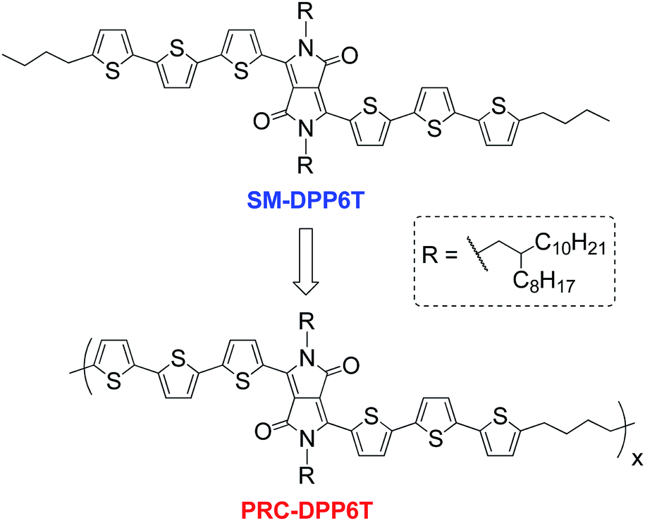 | ||
| Scheme 1 Chemical structures of SM-DPP6T and PRC-DPP6T. | ||
Experimental section
Materials and characterization methods
The syntheses of SM-DPP6T and PRC-DPP6T are shown in Scheme 2 and experimental details can be found in the ESI.†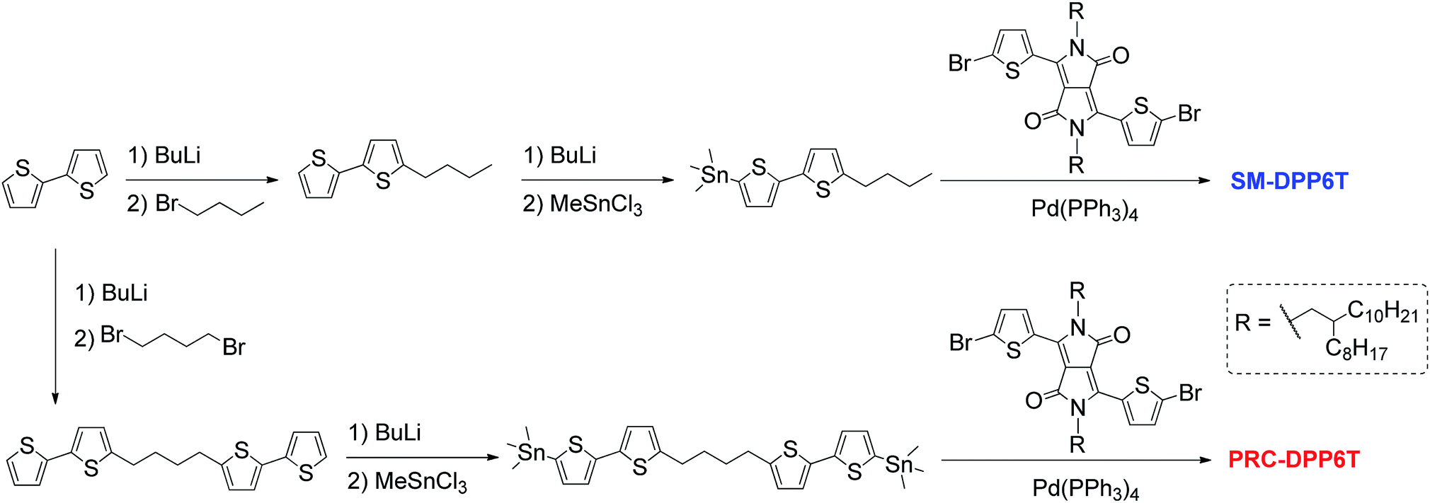 | ||
| Scheme 2 Synthetic routes of SM-DPP6T and PRC-DPP6T. | ||
Device fabrication and characterization
A bottom-gate-top-contact OFET device configuration was used to characterize charge transport properties of SM-DPP6T and PRC-DPP6T. Devices were fabricated on heavily p+-doped Si wafers with a thermally grown silicon oxide layer (∼300 nm) having a resistivity of 0.005–0.020 ohm cm, in which p+-Si served as gate electrode while the silicon oxide layer acted as gate dielectric. Prior to use, SiO2/Si wafers were first cleaned by ultrasonication in deionized water for 5 min, and then subjected to the treatment with a Piranha solution composed of 2/1 (v/v) H2SO4 and H2O2 at 90 °C for 15 min. After washed with de-ionized water for three times, the wafers were further cleaned by sequential ultrasonications in de-ionized water, acetone, and isopropanol for 5 min in each step. Then, the wafers were dried with nitrogen flow and heating at 90 °C for 1 h under vacuum. Afterwards, octadecyltrichlorosilane (OTS) treatment was carried out by dropping a few OTS drops on wafer surfaces and placing in an oven at 120 °C for 3 h under vacuum. After sequentially cleaned by ultrasonication in chloroform, heptane, acetone, and isopropanol for 5 min each, the wafers were dried again using nitrogen flow. Onto these OTS-treated wafers, the active layers were fabricated by spin-coating chlorobenzene solutions of PRC-DPP6T and SM-DPP6T (5 mg mL−1) at 2000 rpm for 30 s under ambient conditions. Source/drain contacts (50 nm-thick gold) were then deposited by vacuum deposition through a shadow mask and finished the device fabrication. The so-prepared devices had a channel length (L) of 273 μm and a channel width (W) of 31 μm. If needed, thermal annealing was performed on devices at desired temperature for 30 min under nitrogen.The evaluation of transistor performance was carried out under ambient conditions using a Keithley 4200 semiconductor characterization system. The carrier mobility in the saturated regime, μsat, is calculated according to the below equation:
| IDS = Ciμsat(W/2L)(VG − VT)2 |
Results and discussions
As shown in Scheme 2, the synthesis of PRC-DPP6T was started from 2,2′-bithiophene. It was lithiated with n-BuLi and further reacted with 1,4-dibromobutane, affording 1,4-butylene-linked bis(2,2′-bithiophene). Then, the compound was stannylated with the aid of n-BuLi and converted into one of important monomers for PRC-DPP6T synthesis. Finally, this monomer was Stille-coupling polymerized with 3,6-bis(5-bromothienyl)-1,4-diketopyrrolo[3,4-c]pyrrole. The obtained crude polymer was purified by Soxhlet solvent extraction with methanol, hexane, acetone and chloroform subsequently and finally subjected to size-exclusion chromatography using a column packed with Bio-Bead S-X1 beads to discard low molecular weight fraction. The finally afforded PRC-DPP6T polymer was found to have a number-average molecular weight (Mn) of 14.4 kDa and a polydispersity index (Đ) of 1.98 (Fig. S6†). Meanwhile, the small molecular reference compound, SM-DPP6T, was prepared by the similar Stille coupling reaction and structurally identified by 1H NMR (Fig. S7†), 13C NMR (Fig. S8†), and mass spectroscopy (Fig. S9†).Thermogravimetric analysis (TGA) and differential scanning calorimetry (DSC) were used to evaluate thermal properties of PRC-DPP6T and SM-DPP6T. It is found that both PRC-DPP6T and SM-DPP6T possess good thermal stability under N2 atmosphere, with 5%-weight-loss decomposition temperature (Td) above 400 °C (Fig. S10† and Table 1). In the second heating–cooling cycle of DSC measurement (Fig. 1a and Table 1), a sharp endothermic peak at 131 °C and an intense exothermic peak at 104 °C were observed for SM-DPP6T. Optical microscopy further confirmed that these phase transitions are melting and thermal crystallization process respectively. This indicates that SM-DPP6T, like most reported small molecular semiconductors, is a crystalline material at room temperature. Of interest, a melting transition around 167 °C and a thermal crystallizing transition around 160 °C still appeared in the DSC profile of PRC-DPP6T during heating and cooling processes, respectively. Moreover, an additional exothermic peak around 64 °C may be assignable to glass transition induced by side chain solidification. This complicate phase-transition behaviour suggests that PRC-DPP6T does not resemble conventional 1,4-diketopyrrolo[3,4-c]pyrrole (DPP)-based conjugated polymers, in which no any thermal transitions were observed in the most cases.44–48 The presence of melting/thermal crystallization transition provides the material a potential of melt processing in device fabrication. Since no any solvent is involved, such processing technology is simple, cost-effective, and environmentally benign, and thus extremely welcomed in industry.
| Td (°C) | Tm (°C) | λmax (nm) | λfilm,onset (nm) | Eg,opta (eV) | Eox,onset (V vs. Ag/Ag+) | EHOMOb (eV) | ELUMOc (eV) | ||
|---|---|---|---|---|---|---|---|---|---|
| Solution | Film | ||||||||
| a Eg,opt = 1240/λfilm,onset.b EHOMO = −4.8 + EFc/Fc+ − Eox,onset.c ELUMO = EHOMO + Eg,opt. | |||||||||
| SM-DPP6T | 401 | 131 | 388, 614, 653 | 391, 586, 633, 704 | 764 | 1.62 | 0.64 | −5.34 | −3.72 |
| PRC-DPP6T | 410 | 167 | 390, 620, 664 | 413, 645, 712, 823 | 877 | 1.41 | 0.57 | −5.27 | −3.83 |
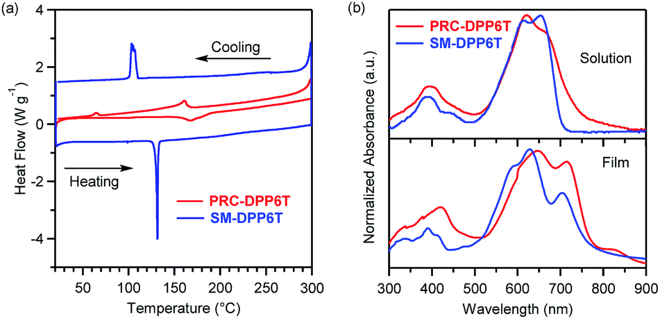 | ||
| Fig. 1 (a) The second heating/cooling traces in DSC profiles of PRC-DPP6T and SM-DPP6T at a temperature ramping rate of 10 °C min−1 under N2 atmosphere, (b) normalized UV-vis absorption spectra of PRC-DPP6T and SM-DPP6T in chlorobenzene solution and film state. | ||
Fig. 1b displays UV-vis absorption spectra of PRC-DPP6T and SM-DPP6T in solution and film state with their absorption peaks summarized in Table 1. In dilute chlorobenzene (CB) solution, SM-DPP6T showed an intense absorption spectrum in the range of 300–700 nm with peak-tops at 653, 614, and 388 nm. Concentration-dependent UV-vis spectroscopy (Fig. S11†) revealed that the absorbance of these peaks obey Beer–Lambert law very well, indicating all these peaks originate from single molecule of SM-DPP6T. With further reference to literature reports,49–52 the peaks at 653 and 614 nm can be assignable to 0–0 and 0–1 vibration bands of intramolecular charge transfer (ICT) between DPP accepting unit and oligothiophene donor moieties, while the peaks around 388 nm are due to local π–π* transitions. In film state, the ICT peaks hypochromatically shifted to 633 and 586 nm. Meanwhile, a new absorption peak at 704 nm was observed, which would come from intermolecular π–π stacking interactions. All these spectral changes suggest that SM-DPP6T forms H-aggregates53 in solid state. Compared with SM-DPP6T, PRC-DPP6T displayed a similar ICT band in solution but in slightly red-shifted region with two peak-tops at 664 and 620 nm and a larger FWHM (full width at half maximum). Although concentration-dependent spectroscopy (Fig. S11†) again confirms that these absorption features are coming from single chain of the polymers, the red shifts in peaktops and the broadness of ICT band implies the existence of certain specific interactions among conjugated segments of single strand polymer even in diluted solution. In film state, these ICT peaks of PRC-DPP6T changed to 712 and 645 nm, having a red shift of 48 and 25 nm, respectively, as reference to their solution spectrum. Moreover, a new peak corresponding to π–π interactions among conjugated segments from different or even the same polymer chains appeared at 823 nm in film state. These observations indicate that PRC-DPP6T, unlike SM-DPP6T, undergoes J-aggregation53 in solid state. Furthermore, such contrary spectral shifts of PRC-DPP6T and SM-DPP6T in film state also afforded quite difference in onset absorption point, in which that of PRC-DPP6T (877 nm) is about 100 nm red-shifted to that of SM-DPP6T (764 nm). As a result, PRC-DPP6T showed a slightly narrower bandgap than SM-DPP6T (1.41 vs. 1.62 eV).
Cyclic voltammetry (CV, Fig. S12†) was used to evaluate electronic energy levels of PRC-DPP6T and SM-DPP6T. Both materials displayed an intense oxidative peak in the positive scanning with an onset point of 0.57 and 0.64 V vs. Ag/Ag+ for PRC-DPP6T and SM-DPP6T, respectively (Table 1). Based on the facts that the absolute energy level of ferrocene/ferrocenium (Fc/Fc+) is −4.80 eV from vaccum54–56 and its redox couple (EFc/Fc+) was estimated to be 0.098 V under the same conditions, the highest occupied molecular orbital (HOMO) energy levels of PRC-DPP6T and SM-DPP6T were calculated to be −5.27 and −5.34 eV, respectively. From these HOMO and previous optical bandgap data, the energy level of the lowest unoccupied molecular orbital (LUMO) was estimated to be −3.83 eV for PRC-DPP6T and −3.72 eV for SM-DPP6T. Therefore, both materials possess similar electronic energy levels with low-lying HOMO and LUMO levels, indicating both of them have potential to be used as hole- and electro-conducting semiconductors.
Film formation capability is critical to a material for achieving high device fabrication rate. In this work, we evaluated this capability of PRC-DPP6T and SM-DPP6T by spin-coating their chlorobenzene (CB), chloroform (CF), and o-dichlorobenzene (o-DCB) solutions with a concentration of 5 mg mL−1 onto octadecyltrichlorosilane (OTS)-treated SiO2/Si wafers. Optical microscopy (OM) found that PRC-DPP6T can form a smooth film irrespective of which solvent was used (Fig. 2). Raman reflective mapping at 1516 cm−1 on three different areas further confirmed the homogeneous distribution of PRC-DPP6T on these films (Fig. 2). In sharp contrast, many aggregates were found in OM pictures of SM-DPP6T films spin-coating from its CB or CF solution. Raman reflective mapping further demonstrated uneven distribution of SM-DPP6T on these films. Moreover, when o-DCB was used as solvent, all attempts to form a naked eye-distinguished SM-DPP6T film failed (Fig. 2). All these experiments clearly indicate that PRC-DPP6T possesses a much better film formation capability than SM-DPP6T.
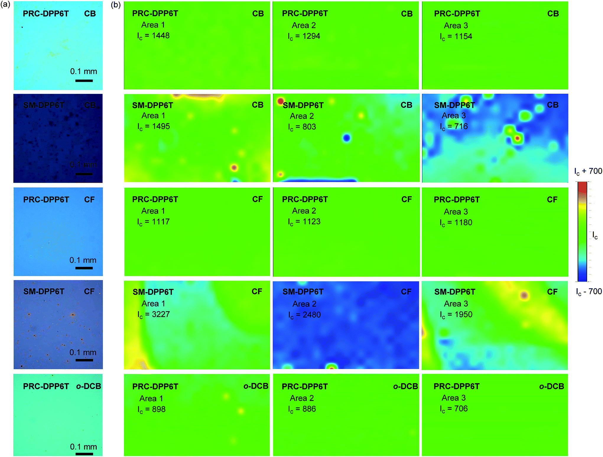 | ||
| Fig. 2 (a) Optical microscope images, (b) reflective Raman mapping (600 × 360 μm2) at 1516 cm−1 of PRC-DPP6T and SM-DPP6T films spin-coated from various solutions. The parameter Ic in (b) is the average Raman intensity between the largest and the smallest values for the mapping area. | ||
In order to quantitatively identify the difference in this film formation capability; we statistically investigated surface coverage on ∼50 piece samples prepared from CB solutions (Fig. 3a). The parameter of surface coverage was estimated by comparing the total area of the surface having sample on it to the whole surface area of the SiO2/Si wafer (∼10 × 10 mm2). Of interest, it was found that all the checked PRC-DPP6T samples possessed a fully covered surface. However, only 20% SM-DPP6T samples displayed a surface coverage larger than 95%, and as large as 46% SM-DPP6T samples had a surface coverage less than 5%. Obviously, samples with a surface coverage less than 95% could not produce qualified OFET devices in practice and thus are not applicable for device fabrication. Therefore in this work, only the samples having a surface coverage of >95% were used for OFET device fabrication. After checking the performances of these as-prepared OFETs, we got a distribution in mobility of SM-DPP6T devices, ranging from 0.002 to 0.055 cm2 V−1 s−1 (Fig. 3b). This distribution became narrow into a range of 0.002–0.012 cm2 V−1 s−1 in the case of PRC-DPP6T. The result is not surprising since it is closely associated with the aforementioned uneven surface coverage for SM-DPP6T on modified SiO2/Si. Again, it confirms poly(rod-coil) polymer, PRC-DPP6T, possesses better film formation property than SM-DPP6T, and thus has a much higher potential to produce qualified OFET devices and with reproducible performance.
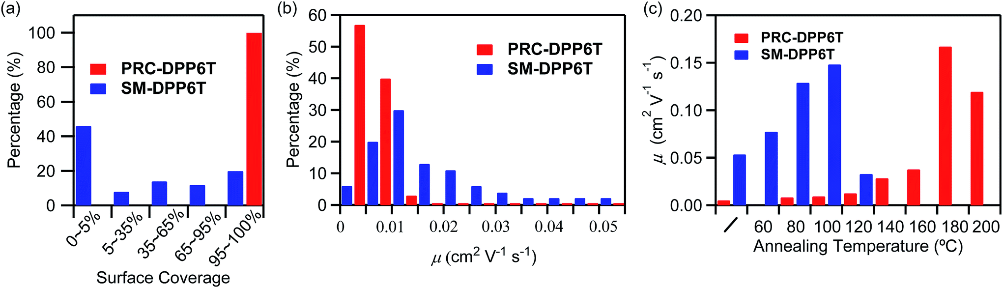 | ||
| Fig. 3 (a) Surface coverage distributions of ∼50 pieces samples; (b) hole mobility distributions of ∼30 devices of PRC-DPP6T and SM-DPP6T films prepared from spin-coating their CB solutions onto OTS-treated SiO2/Si wafers; (c) mobility changes of their best devices subjected to thermal annealing at various temperatures. | ||
Although PRC-DPP6T displayed much better film formation properties and showed a high device fabrication success rate than SM-DPP6T, the best performance of its as-prepared devices lagged behind SM-DPP6T devices. Since device performance is highly dependent on molecular π–π packing in the active layer, step thermal annealing was applied on both SM-DPP6T and PRC-DPP6T devices to optimize such packing structures (Fig. 3c, Table 2, Fig. S13 and S14†). Initially, the as-prepared SM-DPP6T device exhibited a mobility of 0.054 cm2 V−1 s−1. Its mobility was gradually enhanced to 0.079 and 0.13 cm2 V−1 s−1 after step thermal annealing at 60 °C and 80 °C for 30 min, respectively. The best performance was achieved after further annealing at 100 °C for 30 min and reported a mobility of 0.15 cm2 V−1 s−1. However, when the device was further annealed at 120 °C, its mobility quickly dropped to 0.034 cm2 V−1 s−1. In comparison, PRC-DPP6T device displayed an initial mobility of 0.0054 cm2 V−1 s−1, one order lower than that of SM-DPP6T device. Step thermal annealing also improve device performance gradually and finally reached 0.17 cm2 V−1 s−1 after annealing at 180 °C. This value is comparable to that of SM-DPP6T device (0.15 cm2 V−1 s−1). Further rising the temperature to 200 °C led to slightly dropping its mobility to 0.12 cm2 V−1 s−1. This result is interesting when considering PRC-DPP6T device initially showed a poor performance than SM-DPP6T device, but finally overbid the latter after thermal annealing. More importantly, the PRC-DPP6T device achieved its best performance at a temperature of 180 °C, much higher than that for small molecule-based device (100 °C), implying the device of PRC-DPP6T would possess a much higher heat-resistant property than that based on SM-DPP6T.
| Devices | Tannealing (°C) | μmax (μavg)a (cm2 V−1 s−1) | Ion/Ioff | VTh,avg (V) |
|---|---|---|---|---|
| a Data in parenthesis are average values based on around 12 devices.b As cast devices. | ||||
| PRC-DPP6T | —b | 0.0054 (0.0046) | 104–105 | −6.83 |
| 80 | 0.0086 (0.0063) | 104–105 | −6.90 | |
| 100 | 0.0096 (0.0072) | 104–105 | −8.39 | |
| 120 | 0.013 (0.011) | 104–105 | −16.14 | |
| 140 | 0.029 (0.023) | 105–106 | −13.59 | |
| 160 | 0.038 (0.028) | 105–106 | −9.27 | |
| 180 | 0.17 (0.14) | 105–106 | −12.91 | |
| 200 | 0.12 (0.099) | 105–106 | −12.16 | |
| SM-DPP6T | —b | 0.054 (0.039) | 103–104 | −13.02 |
| 60 | 0.079 (0.068) | 104–105 | −8.03 | |
| 80 | 0.13 (0.12) | 104–105 | −10.16 | |
| 100 | 0.15 (0.13) | 104–105 | −10.22 | |
| 120 | 0.034 (0.024) | 104–105 | −2.41 | |
In order to understand the changes in chain/molecular packing structure, π–π interactions, and film morphology during step thermal annealing processes, X-ray diffraction (XRD), temperature-dependent UV-vis absorption spectroscopy, and atomic force microscopy (AFM) were carried out. As shown in Fig. 4b, the as-casted SM-DPP6T film exhibited a set of diffraction peaks at 4.47, 9.02, and 18.28° having d-spacing of 1.974, 0.979, and 0.485 nm, respectively. These peaks can be assigned to 100, 200 and 400 diffraction of a lamellar structure with a layer distance of 1.97 nm. Besides these peaks, a broad and weak peak appeared at 22.9° with a d-spacing of 0.39 nm, which comes from 010 diffraction and suggests the existence of face-to-face π–π stacking among molecules. When the film was subjected to step annealing, the 100 peak became more and more sharp and slight shifted to small diffraction angle. Moreover, after annealing at 100 °C, the film clearly displayed a set of new diffraction peaks around 10.24 and 20.68° with d-spacing of 0.86 and 0.43 nm, respectively, suggesting the possibly rising of new order in a new crystalline dimension. All these observations indicate that thermal annealing improves the crystalline order of SM-DPP6T, and thus account for its performance improvement in charge transportation. In comparison, the XRD profile of as-casted PRC-DPP6T film shows a set of diffraction peaks at 6.0, 12.0, and 17.6° with d-spacing of 1.47, 0.74, and 0.50 nm, respectively (Fig. 4a). These also suggest the chains of PRC-DPP6T formed a lamellar structure with layer distance of 1.47 nm. When the film was subjected to stepwise thermal annealing at 80, 100, 120, and 140 °C, the 100 peak became broader and broader. Further thermal annealing at 160, 180 and 200 °C resulted in the rising of a new peak at 5.5° and the vanish of the peak around 6.6°, implying the reorganization in its chain packing structure under such high temperature annealing. However, all these can't well explain the performance improvement for PRC-DPP6T film after thermal annealing. Fortunately, besides these changes, a broad peak around 22.3° appeared after 120 °C annealing and kept clearly visible even after 200 °C annealing. This peak has a d-spacing of 0.40 nm and could be closely associated to π–π stacking structure among the polymer chains. Therefore, it indicates that thermal annealing promotes PRC-DPP6T chains form a more favourable regular packing structure to facilitate the occurrence of π–π interactions, and thus improves its OFET performance.
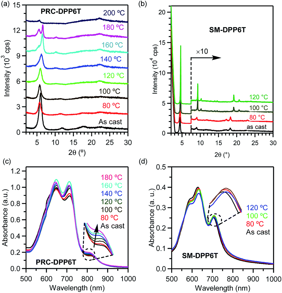 | ||
| Fig. 4 (a and b) XRD profiles of (a) PRC-DPP6T and (b) SM-DPP6T films on OTS-modified Si/SiO2 wafers in as-cast condition and after thermal annealing at various temperatures. (c and d) UV-vis absorption spectra of (c) PRC-DPP6T and (d) SM-DPP6T films on quartz plates in as-cast condition and after thermal annealing at various temperatures. Insets show their enlarged regions for π–π interactions. | ||
Fig. 4c and d display UV-vis absorption spectra of PRC-DPP6T and SM-DPP6T films upon step thermal annealing. It is found that the absorbance of π–π interaction peak for PRC-DPP6T (around 823 nm) increased with the elevation of thermal annealing temperature. This indicates thermal annealing can promote π–π interactions among conjugated segments in PRC-DPP6T. But in the case of SM-DPP6T, the situation became a little complicated. When the film was step annealed at 80 °C and then 100 °C, the absorbance of its π–π interaction peak (704 nm) displayed gradual enhancement. This observation also suggests thermal annealing can enhance π–π interaction peak among SM-DPP6T molecules. But when the film was further treated at 120 °C, the absorbance of the whole spectrum including that of π–π interaction peak decreased. This may be closely related to the formation of big crystals here and there in the film, as evidenced in the bellow AFM observation, which resulted in uneven distributed film thickness. And, it is valuable to point out that the vertex of this π–π interaction peak slightly redshifted upon thermal annealing, from 704 nm for as cast to 706 nm after annealed at 80 °C, then to 708 nm after annealed at 100 and 120 °C. It would be another proof for the reinforcement of π–π interactions among the molecules after thermal annealing.
In AFM microscopy (Fig. 5), the as-casted PRC-DPP6T film on OTS-treated Si/SiO2 wafer displayed a structureless topographical height image with a root-mean-square (RMS) roughness of 7.12 nm. When this film was subjected to thermal annealing, the RMS roughness changed to 3.53 nm at 80 °C, 1.99 nm at 120 °C, and then to 1.34 nm at 140 °C, proving the film became smoother and smoother. After further annealing at 160 and 180 °C, fibrillary aggregates developed and the film became rougher with RMS roughness of 1.36 and 2.47 nm, respectively. Since fibre structures are generally good for charge transportation, it is reasonable to observe mobility enhancement for this PRC-DPP6T film upon thermal annealing. However, when the annealing temperature reached 200 °C, homogeneous and continuous topography disappeared. Alternatively, particle-like morphology was observed in place. Obviously, such film is unfavourable for FET performance, and thus cause performance drop. Since the melting point of PRC-DPP6T is 167 °C as measured by DSC, this morphology change may be closely associated with such melting behaviour. In comparison, the AFM image of as-casted SM-DPP6T film on OTS-treated Si/SiO2 wafer was full of particle (could be assigned to nanocrystals)-like species. Such particles grew bigger when the film was annealed at 60 °C, and then started to merge together at 80 and 100 °C. During these annealing processes, the surface RMS roughness changed from 1.40 nm for as cast film, to 2.69 nm for 60 °C annealing, then to 2.12 and 1.57 nm for annealing at 80 and 100 °C respectively. Higher annealing at 120 °C caused an amazing change in film morphology, which was full with big crystalline objects having clear edges. This made the film not consecutive anymore and resulted in dramatically drop in its FET performance. Since this annealing temperature (120 °C) is close to SM-DPP6T melting point (131 °C measured by DSC), such behaviours are reasonably correlated with melting properties of the material.
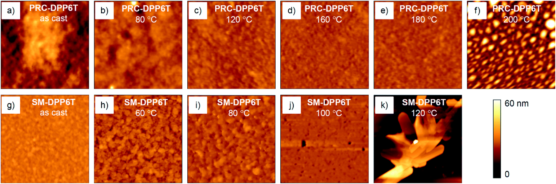 | ||
| Fig. 5 AFM topographical height images (5 × 5 μm2) of (a–f) PRC-DPP6T and (g–k) SM-DPP6T films on OTS-treated Si/SiO2 wafers after annealing at various temperatures. | ||
Conclusions
In summary, a poly(rod-coil) strategy has been demonstrated here to improve film formation properties for small molecular field-effect transistors without sacrifice in mobility. As a typical example of small molecular semiconductors, SM-DPP6T is suffering from the difficulty in formation of homogeneous films on OTS-treated Si/SiO2 with even-distributed active material, and thus hard to ensure fabrication success rate for its OFET device preparation. Furthermore, even for the fabricated devices based on those films having a surface coverage > 95%, an extremely wide mobility distribution has been found. However, all these shortages can be overcome by interconnecting its conjugated core segments with flexible butylene chains and changing its structure into poly(rod-coil) polymer. More interestingly, the resultant poly(rod-coil) polymer, PRC-DPP6T, achieved a mobility up to 0.17 cm2 V−1 s−1, which is comparable to the best performance of SM-DPP6T devices (0.15 cm2 V−1 s−1). Moreover, the change to poly(rod-coil) polymer also enhance material melting point, which lead to an improved heat-resistant property for the devices. Considering a huge number of small molecular organic semiconductors reported in literature, this poly(rod-coil) strategy would open a new avenue for design and development of new polymeric types of organic semiconductors, which are highly potential to combine the merits of both small molecular and polymer materials: definite optoelectronically active conjugated core structure and good film formation property.Conflicts of interest
There are no conflicts to declare.Acknowledgements
This work was financially supported by National Natural Science Foundation of China (No. 21474129, 21674125, and 51761145043), International Science and Technology Cooperation Program of China (No. 2015DFG62680), Strategic Priority Research Program of Chinese Academy of Sciences (No. XDB20020000), Science and Technology Open Cooperation Projects of Henan Province (No. 162106000018 and 172106000067) and Zhengzhou Institute of Technology. The authors thank BL14B1 beam line of Shanghai Synchrotron Radiation Facility.Notes and references
- D. Brage and G. Horowitz, Adv. Mater., 2009, 21, 1473 CrossRef.
- J. E. Anthony, A. Facchetti, M. Heeney, S. Marder and X. Zhan, Adv. Mater., 2010, 22, 3876 CrossRef PubMed.
- C. Wang, H. Dong, W. Hu, Y. Liu and D. Zhu, Chem. Rev., 2012, 112, 2208 CrossRef PubMed.
- H. Dong, X. Fu, J. Liu, Z. Wang and W. Hu, Adv. Mater., 2013, 25, 6158 CrossRef PubMed.
- Y. Zhao, Y. Guo and Y. Liu, Adv. Mater., 2013, 25, 5372 CrossRef PubMed.
- H. Sirringhaus, Adv. Mater., 2014, 26, 1319 CrossRef PubMed.
- X. Gao and Y. Hu, J. Mater. Chem. C, 2014, 2, 3099 RSC.
- H. Chen, Chin. J. Org. Chem., 2016, 36, 460 CrossRef.
- Y.-J. Cheng, S.-H. Yang and C.-S. Hsu, Chem. Rev., 2009, 109, 5868 CrossRef PubMed.
- A. Mishra and P. Bäuerle, Angew. Chem., Int. Ed., 2012, 51, 2020 CrossRef PubMed.
- H. Ye, W. Li and W. Li, Chin. J. Org. Chem., 2012, 32, 266 CrossRef.
- L. Dou, Y. Liu, Z. Hong, G. Li and Y. Yang, Chem. Rev., 2015, 115, 12633 CrossRef PubMed.
- L. Lu, T. Zheng, Q. Wu, A. M. Schneider, D. Zhao and L. Yu, Chem. Rev., 2015, 115, 12666 CrossRef PubMed.
- H. Yao, L. Ye, H. Zhang, S. Li, S. Zhang and J. Hou, Chem. Rev., 2016, 116, 7397 CrossRef PubMed.
- A. C. Grimsdale, K. L. Chan, R. E. Martin, P. G. Jokisz and A. B. Holmes, Chem. Rev., 2009, 109, 897 CrossRef PubMed.
- K. T. Kamtekar, A. P. Monkman and M. R. Bryce, Adv. Mater., 2010, 22, 572 CrossRef PubMed.
- S. Gong, C. Yang and J. Qin, Chem. Soc. Rev., 2012, 41, 4797 RSC.
- X. Yang, G. Zhou and W.-Y. Wong, Chem. Soc. Rev., 2015, 44, 8484 RSC.
- F. Wang, Y. Tao and W. Huang, Acta Chim. Sin., 2015, 73, 9 CrossRef.
- C. Zhang, P. Chen and W. Hu, Small, 2016, 12, 1252 CrossRef PubMed.
- X. Zhan, A. Facchetti, S. Barlow, T. J. Marks, M. A. Ratner, M. R. Wasielewski and S. R. Marder, Adv. Mater., 2011, 23, 268 CrossRef PubMed.
- B. J. Jung, N. J. Tremblay, M.-L. Yeh and H. E. Katz, Chem. Mater., 2011, 23, 568 CrossRef.
- C. B. Nielsen, M. Turbiez and I. McCulloch, Adv. Mater., 2013, 25, 1859 CrossRef PubMed.
- E. Wang, W. Mammo and M. R. Andersson, Adv. Mater., 2014, 26, 1801 CrossRef PubMed.
- Q. Miao, Adv. Mater., 2014, 26, 5541 CrossRef PubMed.
- H. Minemawari, T. Yamada, H. Matsui, J. Tsutsumi, S. Haas, R. Chiba, R. Kumai and T. Hasegawa, Nature, 2011, 475, 364 CrossRef PubMed.
- B. Sun, W. Hong, Z. Yan, H. Aziz and Y. Li, Adv. Mater., 2014, 26, 2636 CrossRef PubMed.
- G. Kim, S.-J. Kang, G. K. Dutta, Y.-K. Han, T. J. Shin, Y.-Y. Noh and C. Yang, J. Am. Chem. Soc., 2014, 136, 9477 CrossRef PubMed.
- J.-H. Dou, Y.-Q. Zheng, Z.-F. Yao, T. Lei, X. Shen, X.-Y. Luo, Z.-A. Yu, S.-D. Zhang, G. Han, Z. Wang, Y. Yi, J.-Y. Wang and J. Pei, Adv. Mater., 2015, 27, 8051 CrossRef PubMed.
- J. Y. Back, H. Yu, I. Song, I. Kang, H. Ahn, T. J. Shin, S.-K. Kwon, J. H. Oh and Y.-H. Kim, Chem. Mater., 2015, 27, 1732 CrossRef.
- M. Yamagishi, J. Takeya, Y. Tominari and Y. Nakazawa, Appl. Phys. Lett., 2007, 90, 182117 CrossRef.
- H.-R. Tseng, H. Phan, C. Luo, M. Wang, L. A. Perez, S. N. Patel, L. Ying, E. J. Kramer, T.-Q. Nguyen, G. C. Bazan and A. J. Heeger, Adv. Mater., 2014, 26, 2993 CrossRef PubMed.
- O. D. Jurchescu, M. Popinciuc, B. J. v. Wees and T. T. M. Palstra, Adv. Mater., 2007, 19, 688 CrossRef.
- B. Kang, R. Kim, S. B. Lee, S.-K. Kwon, Y.-H. Kim and K. Cho, J. Am. Chem. Soc., 2016, 138, 3679 CrossRef PubMed.
- H.-J. Li, J.-T. Wang, C.-Y. Mei and W.-S. Li, Chem. Commun., 2014, 50, 7720 RSC.
- W. Shao, L. Liang, X. Xiang, H.-J. Li, F.-G. Zhao and W.-S. Li, Chin. J. Chem., 2015, 33, 847 CrossRef.
- X. Xiang, W. Shao, L. Liang, X.-Q. Chen, F.-G. Zhao, Z. Lu, W. Wang, J. Li and W.-S. Li, RSC Adv., 2016, 6, 23300 RSC.
- A. Gasperini, S. Bivaud and K. Sivula, Chem. Sci., 2014, 5, 4922 RSC.
- A. Gasperini, X. A. Jeanbourquin, A. Rahmanudin, X. Yu and K. Sivula, Adv. Mater., 2015, 27, 5541 CrossRef PubMed.
- Y. Zhao, X. Zhao, Y. Zang, C.-a. Di, Y. Diao and J. Mei, Macromolecules, 2015, 48, 2048 CrossRef.
- Y. Zhao, X. Zhao, M. Roders, G. Qu, Y. Diao, A. L. Ayzner and J. Mei, Chem. Mater., 2015, 27, 7164 CrossRef.
- B. C. Schroeder, Y.-C. Chiu, X. Gu, Y. Zhou, J. Xu, J. Lopez, C. Lu, M. F. Toney and Z. Bao, Adv. Electron. Mater., 2016, 1600104 CrossRef.
- Y. Zhao, X. Zhao, M. Roders, A. Gumyusenge, A. L. Ayzner and J. Mei, Adv. Mater., 2017, 29, 1605056 CrossRef PubMed.
- Y. Li, S. P. Singh and P. Sonar, Adv. Mater., 2010, 22, 4862 CrossRef PubMed.
- Y. Li, P. Sonar, S. P. Singh, M. S. Soh, M. v. Meurs and J. Tan, J. Am. Chem. Soc., 2011, 133, 2198 CrossRef PubMed.
- Y. Li, P. Sonar, S. P. Singh, W. Zeng and M. S. Soh, J. Mater. Chem., 2011, 21, 10829 RSC.
- J. S. Lee, S. K. Son, S. Song, H. Kim, D. R. Lee, K. Kim, M. J. Ko, D. H. Choi, B. Kim and J. H. Cho, Chem. Mater., 2012, 24, 1316 CrossRef.
- C. Li, Z. Mao, H. Chen, L. Zheng, J. Huang, B. Zhao, S. Tan and G. Yu, Macromolecules, 2015, 48, 2444 CrossRef.
- J. Lee, A.-R. Han, H. Yu, T. J. Shin, C. Yang and J. H. Oh, J. Am. Chem. Soc., 2013, 135, 9540 CrossRef PubMed.
- M. J. Cho, J. Shin, S. H. Yoon, T. W. Lee, M. Kaur and D. H. Choi, Chem. Commun., 2013, 49, 7132 RSC.
- J. Y. Back, H. Yu, I. Song, I. Kang, H. Ahn, T. J. Shin, S.-K. Kwon, J. H. Oh and Y.-H. Kim, Chem. Mater., 2015, 27, 1732 CrossRef.
- S. Park, J. Cho, M. J. Ko, D. S. Chung and H. J. Son, Macromolecules, 2015, 48, 3883 CrossRef.
- M. Kirkus, L. Wang, S. Mothy, D. Beljonne, J. Cornil, R. A. J. Janssen and S. C. J. Meskers, J. Phys. Chem. A, 2012, 116, 7927 CrossRef PubMed.
- C.-Y. Mei, L. Liang, F.-G. Zhao, J.-T. Wang, L.-F. Yu, Y.-X. Li and W.-S. Li, Macromolecules, 2013, 46, 7920 CrossRef.
- L. Liang, J.-T. Wang, X. Xiang, J. Ling, F.-G. Zhao and W.-S. Li, J. Mater. Chem. A, 2014, 2, 15396 RSC.
- L. Liang, X.-Q. Chen, L.-N. Liu, J. Ling, X. Xiang, W.-J. Xiao, C.-W. Ge, F.-G. Zhao, G. Xie, Z. Lu, J. Li and W.-S. Li, Tetrahedron, 2016, 72, 4329 CrossRef.
Footnote |
| † Electronic supplementary information (ESI) available. See DOI: 10.1039/c8ra04405h |
| This journal is © The Royal Society of Chemistry 2018 |