
 Open Access Article
 This Open Access Article is licensed under a Creative Commons Attribution-Non Commercial 3.0 Unported Licence
A wide-range operating synaptic device based on organic ferroelectricity with low energy consumption†
Li Tu a,
Sijian Yuana,
Jiawei Xua,
Kunlong Yangb,
Pengfei Wanga,
Xiaolei Cuia,
Xin Zhangc,
Jiao Wanga,
Yi-Qiang Zhan*a and
Li-Rong Zheng*a
a,
Sijian Yuana,
Jiawei Xua,
Kunlong Yangb,
Pengfei Wanga,
Xiaolei Cuia,
Xin Zhangc,
Jiao Wanga,
Yi-Qiang Zhan*a and
Li-Rong Zheng*a
aState Key Laboratory of ASIC and System, SIST, Fudan University, 200433, Shanghai, China. E-mail: yqzhan@fudan.edu.cn; lrzheng@fudan.edu.cn
bSchool of Technology and Health, Royal Institute of Technology, SE-10044, Stockholm, Sweden
cKey Laboratory of Flexible Electronics & Institute of Advanced Materials, Nanjing Tech University, 211800, Nanjing, China
First published on 25th July 2018
Abstract
In this work, a wide-range operating synaptic device based on organic ferroelectricity has been demonstrated. The device possesses a simple two-terminal structure by using a ferroelectric phase-separated polymer blend as the active layer and gold/indium tin oxide (ITO) as the top/bottom electrodes, and exhibits a distinctive history-dependent resistive switching behavior at room temperature. And the device with low energy consumption (∼50 fJ μm−2 per synaptic event) can provide a reliable synaptic function of potentiation, depression and the complex memory behavior simulation of differential responses to diverse stimulations. In addition, using simulations, the accuracy of 32 × 32 pixel image recognition is improved from 76.21% to 85.06% in the classical model Cifar-10 with 1024 levels of the device, which is an important step towards the higher performance goal in image recognition based on memristive neuromorphic networks.
Introduction
With approximately 1014 synapses, the extremely complex human cerebral cortex is difficult to implement on the hardware based on traditional semiconductor integrated circuit technology.1 To provide comparable complexity and manageable power dissipation, hybrid neuromorphic networks composed of complementary metal-oxide semiconductor (CMOS) circuits and adjustable two-terminal resistive devices (synaptic devices) have been proposed.2,3 Unlike conventional von Neumann type computers, these networks enable adaptable and high-efficiency computing by implementing massive parallelism at a physical level.4,5 In biological neural networks, the realization of learning and memory behavior is essentially based on the adjustment of relative synaptic connection strengths (i.e., the synaptic weights) between pre- and postsynaptic neurons.6,7 Similarly in this hybrid neuromorphic network, the synaptic devices which mimic biological synapses can provide a series of weight levels under continuous pulse stimulations. And each value of these weight levels can represent a certain synaptic weight reflecting the relative synaptic connection strength. In this way, the function of the human brain, such as image recognition, can be well realized.1,4For learning more complex input patterns and reducing the error rate of image recognition, wide-range operating (i.e. more levels under continuous pulses) synaptic devices are desperately desired, which have the ability to provide more training epochs.1,8 In a typical training epoch of an artificial neural network, patterns from the training set were applied in the form of voltage pulse, one by one, to the network's input, and its outputs in the form of current value were used to calculate the change of weight (conductance) through a series of training algorithms.1 According to the result, a certain pulse sequence would be applied to the corresponding synaptic device to update weight. The more complex input patterns often need more training epochs in order to meet a higher performance goal (indicated by a smaller error).9 So synaptic device with more weight levels under continuous pulses is becoming a focus of research, attracting a large number of researchers. To achieve these goals, several types of electronic devices based on organic materials with different mechanisms – including redox reaction,10–13 charge trapping and de-trapping,14,15 filamentary switching,16,17 ferroelectric switching18 and ion migration19–22 – have been proposed as a synapse for neuromorphic computing application. In comparison to the inorganic counterparts, the organic devices distinguish themselves with low-cost, easy solution processability, large-area implementation, mechanical flexibility and ductility, and more importantly, tunable electronic properties by designing molecular structure and the possibility of forming self-assembled three dimensional (3D) structures.23–27 In addition, current synaptic device still consume energy that is orders of magnitude greater than biological synapses, and reduction of energy consumption of artificial synapses remains a difficult challenge.20
In this study, a wide-range operating synaptic device based on organic ferroelectricity with low energy consumption is demonstrated. As the fundamental requirements for mimicking biological synapse,28 history-dependent synaptic behaviors of the device were observed in the experiment. In addition to the potentiation and depression of a biological synapse, the complex memory behavior of differential responses to diverse stimulations can also be well simulated with the device. This device can provide 1024 levels under continuous pulses, which are expected to improve the accuracy of 32 × 32 pixel image recognition to 85.06% from 76.21% of 256 levels by using simulations in the classical model Cifar-10. These demonstrations show the possibility of achieving a higher performance goal in image recognition based on memristive neuromorphic networks.
Experimental
Device preparation
The random copolymer of poly(vinylidene fluoride-trifluoroethylene) [P(VDF-TrFE)] (65–35%) and the semiconducting components poly(9,9-dioctylfluorene) (PFO) used in present experiment were commercially available without any further purification. Blend solutions with a concentration of 30 mg ml−1 were prepared by co-dissolving P(VDF-TrFE) and PFO in tetrahydrofuran (THF) (99.8%) at 50 °C. The PFO ratio of P(VDF-TrFE)![[thin space (1/6-em)]](https://www.rsc.org/images/entities/char_2009.gif) :PFO blend films was 10 wt% in weight. The P(VDF-TrFE):PFO (90:10) thin films were spin-coated, then annealed at 140 °C in vacuum for 2 h. Before coating, the blend solution and substrates were preheating to 50 °C and 100 °C respectively. The devices with the thickness of around 390 nm were completed by the evaporation of copper phthalocyanine (CuPc, 50 nm) and gold top contact (Au, 80 nm) through a shadow mask in a vacuum chamber (around 2.0 × 10⁶ Pa) successively. The deposition rate of CuPc and Au was about 0.4 and 0.5 Å s−1 respectively. The device area is 6 mm2.
:PFO blend films was 10 wt% in weight. The P(VDF-TrFE):PFO (90:10) thin films were spin-coated, then annealed at 140 °C in vacuum for 2 h. Before coating, the blend solution and substrates were preheating to 50 °C and 100 °C respectively. The devices with the thickness of around 390 nm were completed by the evaporation of copper phthalocyanine (CuPc, 50 nm) and gold top contact (Au, 80 nm) through a shadow mask in a vacuum chamber (around 2.0 × 10⁶ Pa) successively. The deposition rate of CuPc and Au was about 0.4 and 0.5 Å s−1 respectively. The device area is 6 mm2.
Characterization
All electrical measurements were carried out by the Agilent B1500A semiconductor device analyzer. The voltage pulse and wave signals were generated by Agilent 33220A wave generator and power amplifier.Results and discussion
Organic ferroelectric materials, represented by P(VDF-TrFE), distinguish themselves with its relatively low crystallization temperature (∼140 °C), a relatively large remanent polarization and a short switching time.29 When blending the insulating ferroelectric P(VDF-TrFE) and a semiconducting polymer, a conducting composite with distinct ferroelectric and semiconducting areas can be obtained, which enable an independent tuning of the ferroelectric and conductive properties of the composite film.29 Besides, it was demonstrated that the maximum barrier that can be switched by the P(VDF-TrFE) ferroelectric polarization is 1.6 eV.30 For the PFO/ITO interface, the injection barrier, which is the difference between the ITO work function (∼4.7 eV) and PFO ionization potential (∼6.1 eV), is about 1.4 eV. This relatively high barrier is expected to generate more conductance levels due to a broader adjusting range of the injection barrier progressively polarized by P(VDF-TrFE) component under continuous pulses. On these foundations, a wide-range operating synaptic device with a simple two-terminal structure, by using a ferroelectric phase-separated polymer blend [P(VDF-TrFE) and PFO] as the active layer and Au/ITO as top/bottom electrodes, have been fabricated, which is illustrated schematically in Fig. 1a. More importantly, a layer of CuPc, which is a very robust material, is first used to fill up the rough interface of Au and the polymer blend. The film of CuPc can effectively prevent the previously reported formation of the metallic conducting channels, making the device more stable.31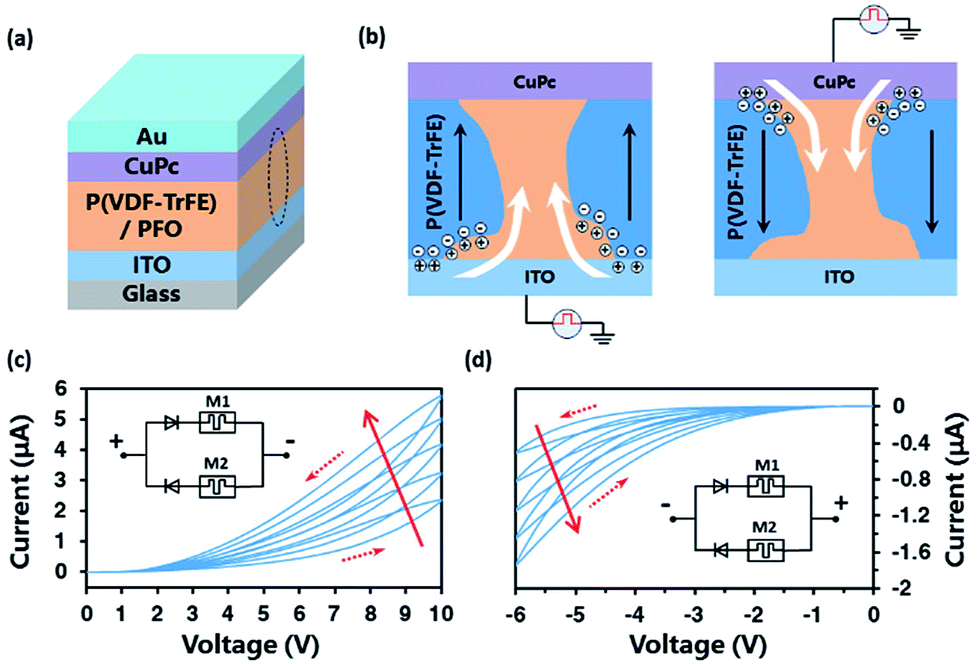 | ||
| Fig. 1 (a) Schematic illustration of the Au/CuPc/P(VDF-TrFE) + PFO/ITO synaptic device. (b) Sketch of the operation mechanism of a polymeric ferroelectric interpenetrating network. Polarization of the ferroelectric phase leads to accumulation of charges in the organic semiconductor domain, which modulates the injection barrier of the semiconductor/electrode interface leading to the change of the device conductance. The positive (c) and negative (d) current–voltage characteristics of the synaptic device showing a distinctive history-dependent resistive switching behavior. The step width of voltage sweeps are 0.15 V and 0.06 V, respectively. Inset: an equivalent circuit model of the device. | ||
The device exhibits a distinctive history-dependent resistive switching behavior at room temperature, as plotted in the current–voltage (I–V) characteristics of Fig. 1c with the Au electrode grounded and the ITO electrode applied with a scanning voltage and of Fig. 1d with the opposite direction. The operation mechanism of a polymeric ferroelectric interpenetrating network is shown in Fig. 1b, the left of which corresponds to Fig. 1c while the right corresponds to Fig. 1d. As for Fig. 1c, the P(VDF-TrFE) component was initially polarized completely in the opposite direction by applying a voltage of −20 V with a period of time. Upon being subjected to each consecutive positive voltage sweep circle of 0 V → 10 V → 0 V at the ITO electrode, the polarization of P(VDF-TrFE) component was enhanced bit by bit. Owing to the poling, a negative polarization charge is built up in the ferroelectric P(VDF-TrFE). To neutralize the polarization charges, holes will accumulate in the semiconducting phase PFO and in the ITO electrode. The band diagram at the ITO electrode along the cross section A-B in Fig. 1b is shown in Fig. S1b of ESI.† The accumulated charge gives rise to strong band bending in the PFO semiconductor, which effectively reduces the injection barrier at the interface between ITO and PFO. The charge injection as indicated by the arrows in Fig. S1b† is then strongly enhanced and the contact becomes ohmic, resulting in the increase of the device conductance.30–32 The same mechanism happens in the CuPc/PFO interface when applied the opposite direction voltage, the result of which is shown in Fig. 1d. And the retention time (over 24 h) of the device based on ferroelectric phase-separated blend have been demonstrated in the ref. 32. That is to say, the main active interface is different under the different direction of applied voltage, which is ITO/PFO interface in Fig. 1c or CuPc/PFO interface in Fig. 1d. So the device can be equivalent to two memristor in series with a respective diode connected in parallel. An equivalent circuit model of the device is shown in Fig. 1c and d inset.
As seen from Fig. 1c and d, both directions of voltage sweeps tends to increase the current. While in the actual training system, each synapse is often implemented with two synaptic devices in order to speed up the convergence process of training algorithm in the system.1 In this case, synaptic weight (W) is characterized by the difference between the effective conductances of these two devices represented as G+ and G− (W = G+ − G−). The increase/decrease of synaptic weight (W) is characterized by the increase of G+/G− which is the conductance of each device. That is to say, as for a single device, only positive I–V characteristics will be used in the training system. In our device, there are two memristive mode M1 and M2 shown in Fig. 1c and d inset, which can be used separately or jointly such as the emulation of a biological synapse in the form of M1–M1, M2–M2 or M1–M2. The injection barrier between CuPc (∼5.3 eV) and PFO (∼6.1 eV) is 0.8 eV, lower than the interface ITO/PFO of 1.4 eV. Thus, M2 (main active interface is CuPc/PFO) has lower operating voltage 6 V and energy consumption (∼50 nJ mm−2 per synaptic event) than M1, while M1 has more levels under continuous pulses. These features make it possible to switch two modes by changing the direction of applied voltage according to needs. Further optimization of device performance can be done from two aspects. One is to reduce the size of device fabricated by lithography technology, and we estimate that a device with area of 0.1 μm2 may use as little as 5 fJ per operation, which is close to a natural synapse (∼10 fJ per operation).20 Another is to optimize the device thickness and structure, which can decrease both energy consumption and operating voltage. Besides, for high performance in image recognition, the positive mode M1 is used in the following experiment.
The potentiation and depression of biological synapse, which are considered as the neurobiological basis of the human brain memory functions,11 are well simulated with this device. As mentioned before, synaptic weight (W) is characterized by the difference between the effective conductances of two devices represented as G+ and G− (W = G+ − G−). At first, synaptic device G+ was subjected to 200 consecutive positive pulses with the amplitude of 10 V, duration of 50 ms. And then synaptic device G− was immediately subjected to 200 consecutive positive pulses with the same amplitude and duration. The change trend of W in the whole process is shown in Fig. 2a, which is extremely smooth and stable without significant disturbance. The main reason is due to the relatively good polarization stability of P(VDF-TrFE), and meanwhile it can be polarized progressively under continuous pulses. Obviously, the synaptic connection has been well potentiated or depressed with the consecutive pulses, which lay a good foundation for the emulation of more complex learning and memory behavior.
 | ||
| Fig. 2 (a) The potentiation and depression of synaptic weight W (W = G+ − G−). The relative changes of conductance versus pulse numbers under (b) pulse voltage of 10 to 20 V, pulse width of 500 ms and (c) pulse voltage of 15 V, pulse width of 100 to 900 ms, respectively. | ||
In the human brain, memory strength depends on the way in which the information was learned. This can also be well simulated with the device. Here, the conductance of the device is analogous to the memory state, while the “learning” conditions (i.e., the stimulation conditions) can be varied by changing the pulse number, the pulse voltage and the pulse width.33,34 The influence of the pulse number on the synaptic weight can be seen obviously in the first 200 pulses of Fig. 2a, which resembles the phenomenon that the more stimulations lead to the stronger synaptic connection. In order to demonstrate the effect of the pulse height and pulse width on the synaptic weight, the number of the applied pulses is fixed at a constant of 10 while changing the pulse voltage from 10 to 20 V with constant pulse width of 500 ms and the pulse width from 100 to 900 ms with constant pulse voltage of 15 V, respectively. The relative changes of conductance versus pulse numbers under different pulse voltage or pulse width were plotted in Fig. 2b or c. With the increase of the pulse height or the pulse width, the synaptic weight characterized by conductance of the device increase dramatically. The main reason is that the polarization of P(VDF-TrFE) component is enhanced more greatly under each pulse, leading to a sharply slump in injection barrier of ITO/PFO interface. These demonstrations indicate that synaptic connection depends heavily on the stimulation number and the stimulation strength (i.e., the pulse height and width), similar to the memory behavior of the human brain.
To quantitatively demonstrate the extremely wide-range operating performance, the device was programmed by a series of identical positive pulses with the amplitude of 15 V, duration of 50 ms, and period of 200 ms. Fig. 3a shows continuous response of a single device to the 1024 spike pulses, which has good reproducibility among different devices with the same process parameters. The whole response curve is relatively smooth. During the first 400 pulses, the conductance increases sublinearly and the conductance difference between contiguous levels decreases gradually, the partial detail of which is shown in Fig. 3b. After then the increase of conductance is close to linear while the conductance difference between contiguous levels maintains at around 0.06 μS, which is shown in Fig. 3c. Essentially, the conductance change is attributed to the modulation of the injection barrier polarized by P(VDF-TrFE) component under applied pulse.30–32 When the device was applied pulses continuously, the polarization of P(VDF-TrFE) component can be enhanced easily at first, and then become slowly, which lead to the trend of conductance change.
 | ||
| Fig. 3 (a) The device was programmed by 1024 identical positive pulses with the amplitude of 15 V, duration of 50 ms, and period of 200 ms (b) and (c) the detail of the dashed frames in (a) shows the conductance difference between contiguous levels (ΔGc). | ||
Compared with other three terminals synaptic device based on ferroelectric switching, our device has simpler structure and is more close to biological synapse in morphology. These features make it possible to form higher-density neuromorphic computing networks. Besides, in comparison to other synaptic device with similar structure, this device with comparable energy consumption can provide 1024 levels under continuous pulses, more than all results reported so far.
In order to prove the great benefit of the device with 1024 levels to the image recognition, simulation experiment was carried out with a classical image dataset called Cifar-10 and its neural network model. Cifar-10 has 60000 colorful images of 32 × 32 pixel in 10 classes, 50000 images of which for training and 10000 images for testing.35,36 An example of image recognition with neural network model of 13 layers including five convolution layers is sketched in Fig. 4a. In this simulation experiments, a weight array composed of 145578 weights is obtained at first after a series of training epochs, which brings almost the best recognition accuracy of 89.98% remaining basically unchanged with more training epochs. The weight distribution is shown in Fig. 4b. Then the weight array has been separately density-quantized in different bit (from 6 bit to 14 bit). Density quantization is a type of quantizing method, which is to divide the amount of weight values into equal parts and replace the value in each part with the intermediate.37–39 The typical distributions of 10 bit and 8 bit are shown in Fig. 4c and d respectively. With the decrease of quantization bit, the weight distribution becomes more discrete and dispersed, improving system efficiency at the expense of the recognition accuracy. Finally, we import the processed weight array to the Cifar-10 model and take image recognition test, respectively. Fig. 4e shows the result of recognition accuracy with quantized weight array of different bits. As the number of bits increases from 6 to 14, the recognition accuracy is correspondingly 74.5%, 76.21%, 85.06%, 89.9% and 90.11%, rising rapidly at first and then tending to an upper limit that is almost the best recognition accuracy of the original. 10 bit (corresponding to 1024 levels) with the accuracy of 85.06% is much better than 8 bit (corresponding to 256 levels) with that of 76.21%, while 12 bit is almost close to the original. Obviously, a certain amount of weight levels is indispensable for improving the recognition accuracy.
 | ||
| Fig. 4 (a) An example of image recognition process with neural network model of Cifar-10. The weight distribution of (b) the original, (c) 10 bit quantization and (d) 8 bit quantization. (e) The recognition accuracy during the testing process with the original weight array and quantized weight array of 6 bit to 14 bit. | ||
Conclusions
In conclusion, we have demonstrated a wide-range operating synaptic device with low energy consumption based on organic ferroelectricity for image recognition. The device possesses a simple structure of Au/CuPc/P(VDF-TrFE) + PFO/ITO, which exhibits a distinctive history-dependent resistive switching behavior at room temperature. And a minimum energy consumption as low as ∼50 nJ mm−2 per synaptic event was achieved. We estimate that a device with an area of 0.1 μm2 may use as little as 5 fJ per operation, which is close to a natural synapse. The synaptic connection controlled by the applied pulse's features (number, width and height) has been implemented with the device, which closely emulates the memory behavior and depends heavily on the way in which the information is learned. This device can provide 1024 levels under continuous pulses, which are expected to improve the accuracy of 32 × 32 pixel image recognition to 85.06% from 76.21% of 256 levels by using simulations in the classical model Cifar-10. This is an important step towards a higher performance goal in image recognition based on memristive neuromorphic networks. In further study, more efforts can be focused on optimization of the device thickness and structure for lower energy consumption and wider-range operating performance. With the emerge of synaptic devices with more levels under continuous pulses in the future, the recognition accuracy would be further improved and more complex patterns could be recognized.Conflicts of interest
There are no conflicts to declare.Acknowledgements
This work was supported by the Shanghai Science and Technology Committee (15JC1400101 and 17JC1401300).References
- M. Prezioso, F. Merrikh-Bayat, B. D. Hoskins, G. C. Adam, K. K. Likharev and D. B. Strukov, Nature, 2015, 521, 61–64 CrossRef PubMed.
- K. K. Likharev, Sci. Adv. Mater., 2011, 3, 322–331 CrossRef.
- K. K. Likharev and J. Nanoelectron, Optoelectronics, 2008, 3, 203–230 Search PubMed.
- S. Kim, J. Yoon, H. D. Kim and S. J. Choi, ACS Appl. Mater. Interfaces, 2015, 7, 25479–25486 CrossRef PubMed.
- C. J. Wan, L. Q. Zhu, X. Wan, Y. Shi and Q. Wan, Appl. Phys. Lett., 2016, 108(4), 382001 CrossRef.
- D. O. Hebb, The organization of behavior; a neuropsychological theory, John Wiley, Chapman & Hall, 1949 Search PubMed.
- G. Buzsáki, Rhythms of the Brain, Oxford University Press, 2006 Search PubMed.
- F. Alibart, E. Zamanidoost and D. B. Strukov, Nat. Commun., 2013, 4, 131–140 Search PubMed.
- K. Y. Liu, M. R. Smith, E. C. Fear and R. M. Rangayyan, Biomed Signal Process Control, 2013, 8, 255–262 CrossRef.
- Y. Van De Burgt, E. Lubberman, E. J. Fuller, S. T. Keene, G. C. Faria, S. Agarwal, M. J. Marinella, A. Alec Talin and A. Salleo, Nat. Mater., 2017, 16, 414–418 CrossRef PubMed.
- G. Liu, C. Wang, W. Zhang, L. Pan, C. Zhang, X. Yang, F. Fan, Y. Chen and R. W. Li, Adv. Electron. Mater., 2016, 2, 1–8 Search PubMed.
- X. Yang, C. Wang, J. Shang, C. Zhang, H. Tan, X. Yi, L. Pan, W. Zhang, F. Fan, Y. Liu, Y. Chen, G. Liu and R.-W. Li, RSC Adv., 2016, 6, 25179–25184 RSC.
- C. Zhang, Y.-T. Tai, J. Shang, G. Liu, K.-L. Wang, C. Hsu, X. Yi, X. Yang, W. Xue, H. Tan, S. Guo, L. Pan and R.-W. Li, J. Mater. Chem. C, 2016, 4, 3217–3223 RSC.
- F. Alibart, S. Pieutin, D. Guérin, C. Novembre, S. Lenfant, K. Lmimouni, C. Gamrat and D. Vuillaume, Adv. Funct. Mater., 2010, 20, 330–337 CrossRef.
- H. Y. Choi, C. Wu, C. H. Bok and T. W. Kim, NPG Asia Mater., 2017, 9, e413 CrossRef.
- S. Li, F. Zeng, C. Chen, H. Liu, G. Tang, S. Gao, C. Song, Y. Lin, F. Pan and D. Guo, J. Mater. Chem. C, 2013, 1, 5292 RSC.
- M. K. Hota, M. K. Bera, B. Kundu, S. C. Kundu and C. K. Maiti, Adv. Funct. Mater., 2012, 22, 4493–4499 CrossRef.
- E. J. Kim, K. A. Kim and S. M. Yoon, J. Phys. D: Appl. Phys., 2016, 49, 75105 CrossRef.
- Q. Lai, L. Zhang, Z. Li, W. F. Stickle, R. S. Williams and Y. Chen, Adv. Mater., 2010, 22, 2448–2453 CrossRef PubMed.
- W. Xu, S. Y. Min, H. Hwang and T. W. Lee, Sci. Adv., 2016, 2, e1501326 Search PubMed.
- C. Wu, T. W. Kim, H. Y. Choi, D. B. Strukov and J. J. Yang, Nat. Commun., 2017, 8(1), 752 CrossRef PubMed.
- W. Xu, H. Cho, Y.-H. Kim, Y.-T. Kim, C. Wolf, C.-G. Park and T.-W. Lee, Adv. Mater., 2016, 28, 5916–5922 CrossRef PubMed.
- Y. Chen, G. Liu, C. Wang, W. Zhang, R.-W. Li and L. Wang, Mater. Horiz., 2014, 1, 489 RSC.
- Q. D. Ling, D. J. Liaw, C. Zhu, D. S. H. Chan, E. T. Kang and K. G. Neoh, Prog. Polym. Sci., 2008, 33, 917–978 CrossRef.
- W. P. Lin, S. J. Liu, T. Gong, Q. Zhao and W. Huang, Adv. Mater., 2014, 26, 570–606 CrossRef PubMed.
- B. Cho, S. Song, Y. Ji, T. W. Kim and T. Lee, Adv. Funct. Mater., 2011, 21, 2806–2829 CrossRef.
- J. C. Scott and L. D. Bozano, Adv. Mater., 2007, 19, 1452–1463 CrossRef.
- J. J. Yang, D. B. Strukov and D. R. Stewart, Nat. Nanotechnol., 2013, 8, 13–24 CrossRef PubMed.
- R. C. G. Naber, K. Asadi, P. W. M. Blom, D. M. de Leeuw and B. de Boer, Adv. Mater., 2010, 22, 933–945 CrossRef PubMed.
- K. Asadi, T. G. De Boer, P. W. M. Blom and D. M. De Leeuw, Adv. Funct. Mater., 2009, 19, 3173–3178 CrossRef.
- Y. You, K. Yang, S. Yuan, S. Dong, H. Zhang, Q. Huang, W. P. Gillin, Y. Zhan and L. Zheng, Org. Electron., 2014, 15, 1983–1989 CrossRef.
- K. Asadi, D. M. De Leeuw, B. De Boer and P. W. M. Blom, Nat. Mater., 2008, 7, 547–550 CrossRef PubMed.
- S. G. Hu, Y. Liu, T. P. Chen, Z. Liu, Q. Yu, L. J. Deng, Y. Yin and S. Hosaka, Appl. Phys. Lett., 2013, 103, 1–6 Search PubMed.
- S. Mandal, A. El-Amin, K. Alexander, B. Rajendran and R. Jha, Sci. Rep., 2014, 4(24), 5333 Search PubMed.
- E. F. Carvalho, P. M. Engel and I. S. Engel, Convolutional Sparse Feature Descriptor for Object Recognition in CIFAR-10, 2013, pp. 131–135 Search PubMed.
- J. Gui, T. Liu, Z. Sun, D. Tao and T. Tan, IEEE Trans. Neural Netw. Learn. Syst., 2016, 1–10 Search PubMed.
- J. Qiu, J. Wang, S. Yao, K. Guo, B. Li, E. Zhou, J. Yu, T. Tang, N. Xu and S. Song, Going Deeper with Embedded FPGA Platform for Convolutional Neural Network, 2016, pp. 26–35 Search PubMed.
- S. Han, H. Mao and W. J. Dally, Fibers, 2015, 56, 3–7 Search PubMed.
- E. Alpaydin and A. N. N. Alpaydin, Weight Quantization for Multi-Layer Perceptrons Using Soft Weight Sharing, 2001, pp. 211–216 Search PubMed.
Footnote |
| † Electronic supplementary information (ESI) available. See DOI: 10.1039/c8ra04403a |
| This journal is © The Royal Society of Chemistry 2018 |