DOI:
10.1039/C8RA03950J
(Paper)
RSC Adv., 2018,
8, 29686-29697
Difference in structural and chemical properties of sol–gel spin coated Al doped TiO2, Y doped TiO2 and Gd doped TiO2 based on trivalent dopants
Received
9th May 2018
, Accepted 19th July 2018
First published on 22nd August 2018
Abstract
In this research, pure titanium dioxide (TiO2) and doped TiO2 thin film layers were prepared using the spin coating method of titanium(IV) butoxide on a glass substrate from the sol–gel method and annealed at 500 °C. The effects on the structural and chemical properties of these thin films were then investigated. The metal doped TiO2 thin film which exists as trivalent electrons consists of aluminium (Al), yttrium (Y) and gadolinium (Gd). The anatase phase of the thin films was observed and it was found that the crystal size became smaller when the concentration of thin film increased. The grain size was found to be 0.487 to 13.925 nm. The types of surface morphologies of the thin films were nanoporous, with a little agglomeration and smaller nanoparticles corresponding to Al doped TiO2, Y doped TiO2 and Gd doped TiO2, respectively. The trivalent doping concentration of the thin films increased with a rising of thickness of the thin film. This can contribute to the defects that give advantages to the thin film when the mobility of the hole carriers is high and the electrons of Ti can move easily. Thus, Ti3+ existed as a defect state in the metal doped TiO2 thin film based on lattice distortion with a faster growth thin film that encouraged the formation of a higher level of oxygen vacancy defects.
Introduction
Titanium dioxide (TiO2) is nanomaterial with a vast range of applications for energy production,1 electronics,2 solar devices3 and gas sensors at the nanometre length scale. TiO2 thin films can be obtained using the sol–gel technique, which is a reliable and low-cost chemical route.4 The spin coating method is widely used for the deposition of materials.5 TiO2 is an n-type semiconductor with low conductivity.6 TiO2 materials need to be synthesised with a high surface to bulk ratio with a smaller particle size to attain an efficient contact in the target gas and photocatalytic or photochemical reactions arise on the surface of TiO2.7 Therefore, there has been much effort has been directed to doping TiO2 with metal atoms, where the electrons move from one atom to another atom which causes species with an overall electric charge to be formed.8 Such species are called ions in which the ionic state is 3+, from the metal atoms. Species with overall positive charges are called cations. Therefore, individual Ti atoms losing electrons give monatomic ions, because of the Ti4+ reduction to Ti3+.9 When Ti atoms lose electrons this causes a change of the characteristic number of electrons in which the holes' carrier mobility of the metal is high and the electrons can move easily. Thus, the ionic state of 3+ charges of metal atoms can also modify TiO2, which shows excellent reproducibility.10 The Ti3+ reactions are one of the effects of point defects. Bharti et al. stated that the point defects in terms of charged oxygen vacancies and interstitial titanium ions with three or four charges affect the conductivity of the thin films.11 Xiong et al. reported that Ti3+ plays a role as a defect which increases the conductivity and stability.9 Stability here means the orientation phase of the TiO2 doped with metal. Yang et al. explained that the anatase phase of TiO2 thin film also can also contribute to the stability by controlling its parameter properties.12 There is also an indication that anatase is the most promising phase because of its higher surface reactivity to gases13 and photocatalysts.14
Trivalent dopants need to be used to improve the conductivity, decrease grain growth, increase the crystallinity of the peak and increase the surface area. Xu et al. showed that the defects which existed in TiO2 from a trivalent dopant also contribute excellent results.15 Trivalent dopants which can be used for doping are aluminium (Al),10 gallium (Ga),16 yttrium (Y),17 niobium (Nb)18 and gadolinium (Gd).19 Apart from this, the optimisation of the doping concentration decreases the resistivity of the TiO2 and increases the charge carrier concentration.20
The aim of this research is to introduce Ti3+ as a defect state of the metal doped TiO2 thin film based on the lattice distortion in which the oxygen vacancies have been created. Thus, it is first necessary to study the effects of Al, Y and Gd doping on the structural and chemical properties of the TiO2 thin film. This study discovered that the differences have been attributed to various causes such as doping elements, phase relations, crystal size, chemical elements, structural defects, surface roughness and grain size of the thin film.
Experimental
Firstly, for the substrate preparation, a glass sheet with a size of 2.5 cm × 2.5 cm was cut, and this was used as a substrate. The glass was cleaned with acetone in an ultrasonic bath for 5 min at 50 °C. This cleaning process was needed to remove the organic contamination on the glass substrate surface. After that, the substrate was rinsed in deionized water. Then, the substrate was purged to a dry state with nitrogen gas (N2). The N2 was used to reduce the oxidation, which is established using an inert atmosphere with a very low dew point. The TiO2 sol was prepared using a method reported in previous work. The materials used were titanium(IV) butoxide [Ti(OC4H9)4; Sigma-Aldrich, 97%] as a precursor, ethanol (C2H5OH) as a solvent, deionised water as a source for adding oxygen (O), acids [glacial acetic acid (CH3CO2H) and hydrochloric acid (HCl)] and Triton X-100 (Sigma-Aldrich) as a stabilizer to avoid precipitation in the solution. Titanium(IV) butoxide mixed with ethanol, acid catalysts, Triton X-100 and aluminium nitrate nonahydrate [Al(NO3)3·9H2O; Sigma-Aldrich, ≥98%] were stirred for 3 h (ageing process) using sol–gel synthesis under ambient conditions to obtain the gel at room temperature. Dopant precursors such as aluminium nitrate nonahydrate, yttrium(III) nitrate hexahydrate (N3O9Y·6H2O; Sigma-Aldrich, 99.8%) and gadolinium(III) acetate hydrate (C6H9GdO6·xH2O; Sigma-Aldrich, 99.9%) were added last. All the steps for the undoped sample and doping samples were executed sequentially. A metal ion doped TiO2 solution can be used for the deposition of thin films using the spin-coating method. The acquired sol was spin-coated on the glass substrate at a speed of 3000 rpm over 30 s to deposit five layers of uniform films. The TiO2 solution was dropped up to 10 times onto the substrates. After spin-coating, the layers formed were preheated at 100 °C for 5 min. All the layers were annealed at 500 °C for 1 h to achieve better crystallization. The annealing process was a heat treatment process which altered the microstructure of the material to change its mechanical or electrical properties. After the annealing process, the thin films needed to be cooled in ambient air to room temperature. Finally, the TiO2 thin films were structurally and chemically, characterised.21 The structural properties were characterized using a PAnalytical Smartpowder X-ray diffractometer (XRD). XRD is a non-destructive technique which can be used to detect the crystalline phases of unknown material phases by comparing them with records of the crystal structures of materials in the Inorganic Crystal Structure Database (ICSD). The surface morphologies and cross-sections of the thin films were observed using field emission scanning electron microscopy (FESEM). The surface morphology images were magnified by 200 K and 100 K. The magnification of the thickness images was 100 K. The surface topologies and roughness were characterized using a Park Systems XE-100 atomic force microscope (AFM), at room temperature. In this research, a non-contact mode was used in which the cantilever oscillates almost on the surface of the sample and senses the van der Waals attractive force that causes a frequency move in the resonant frequency of a stiff cantilever. Furthermore, it was also realised that it was necessary to use the information on grain size and roughness of the TiO2 thin film. X-ray Photoelectron Spectroscopy (XPS) surface chemical analysis techniques were used to determine a stoichiometry change of the oxide for the uppermost top layer of the chemical materials' surface.
Results and discussion
Fig. 1 shows the XRD data of the TiO2 thin films, as-deposited undoped thin film and Al doped TiO2 thin film at different doping concentrations. The anatase TiO2 peaks (I41/amd) became smaller with an increase of the Al doping concentration because of the disorder caused by the size of ionic radii of Al3+ and Ti4+. Doping of Al into TiO2 can lead to a crystallite sized anatase TiO2. Thus, this indicates that the crystallite sizes were smaller when compared to the undoped thin films.
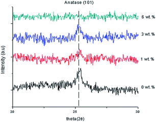 |
| | Fig. 1 XRD data of the undoped thin film and Al doped TiO2 thin film. | |
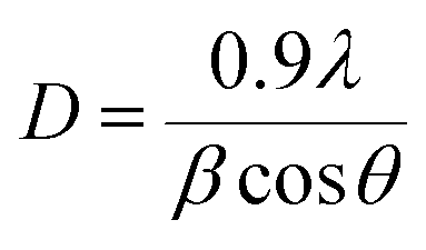
Al doped TiO2 has a smaller average size than the pure TiO2. This phenomenon can be described as the quantum size effect, because the accumulation of Al causes a significant decrease in the crystal size as shown Table 1. The formula of crystal size (D) is simplified as:
| |
 | (1) |
Table 1 Peak properties of Al doped TiO2 thin films at different doping concentrations
| Al doped TiO2 con. |
Position, 2 theta (°) |
Intensity (cts) |
FWHM (°) |
Calculated crystallite size (D, nm) |
Dislocation (×1015) |
Strain |
Stress (GPa) |
Lattice constants |
| a |
c |
| 0 wt% |
25.3735 |
233.83 |
0.36 |
22.62 |
1.954 |
0.147 |
0.34 |
3.7760 |
9.4860 |
| 1 wt% |
25.3574 |
108.8 |
0.3542 |
22.62 |
1.892 |
0.105 |
−0.245 |
3.7800 |
9.5100 |
| 3 wt% |
25.2528 |
103.7 |
0.432 |
18.85 |
2.814 |
0.589 |
1.37 |
3.7960 |
9.4440 |
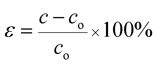
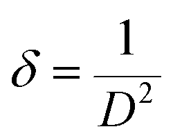
Strain (ε) is defined as the fractional change in length and the dislocation density (δ) is defined as the length of dislocation lines per unit volume of the crystal, and it is measured from the following relationship using the simple approach of Freund and Suresh22 (see eqn (2)).
| |
 | (2) |
| |
 | (3) |
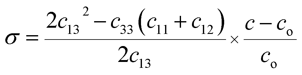
The strain and dislocation density increases with the increase in doping concentration and was attributed to the combination of the atoms in TiO2 in the substitution. The stress (σ) of the prepared thin films is calculated using:22
| |
 | (4) |
where,
c11 = 208.8 GPa,
c33 = 213.8 GPa,
c12 = 119.7 GPa and
c13 = 104.2 GPa.
23 Doping with a larger amount of dopant with 6 wt% of Al caused no characteristic peaks to be observed and the peaks related to Al were not detected, suggesting that Al did not form a significant second phase. This means that the XRD did not detect the dopant phase either, because of the low concentration of Al doping. The samples became amorphous when a higher Al doping concentration was applied. This also applied to the optimisation of Al substitution on the Ti sites. When an atom with a larger atomic radius replaced a small atom in the lattice, it was observed that the peak was shifted towards the lower 2
θ value. The crystallinity of the film influences the transport properties of the photo-generated electrons and holes to the film surface as well as the bandgap energy.
24 A lattice is defined as the periodic arrangement of atoms in the crystal. The smaller the ions or the higher the charge on the ions, the stronger is the attraction between the ions. This creates a strong bond. Lattice energy is the measurement of the strength of the ionic bond. The stronger the ionic bond, the more exothermic is the lattice energy. The lattice energy relies on the size of the ions and the charge on the ions
25 Therefore, during the formation of ionic bonds, the ionization energy required should be low and at the same time the electron affinity should be high, meaning that the reaction is more exothermic. The anatase peak of pure TiO
2 thin film was measured at 25.3735° which corresponded to ICSD file no. 98-002-4276. The anatase peak with 1 wt% Al doping concentration was measured at 25.3574° which corresponded to ICSD file no. 98-020-0392 and the anatase nanocrystalline peak with 3 wt% Al doping concentration was measured at 25.2528° which corresponded to ICSD file no. 98-015-4601.
Table 1 shows the lattice constants and crystallite size of the synthesised samples. The position of 2
θ was shifted to the left and the intensity decreased when the Al doping concentration increased because of the increase in the arrangement of the atoms. In addition, the full width at half maximum (FWHM) became wider and the crystal size decreased because of the increase of the dislocation of the Al doping concentration. When 1 wt% Al doping concentration was applied, the strain of the thin film decreased, so the stress caused a compressive thin film because of the negative sign. However, when 3 wt% Al doping concentration was applied, the strain of the thin film increased, so the stress of the thin film caused a tensile thin film because of the positive sign. Pure TiO
2 has a lattice constant of
a = 3.7760 and
c = 9.4860. The lattice of
a and
c were changed to
a = 3.7960 and
c = 9.4440 when Al doping concentration 3 wt% was applied. Doping Al atoms increased the lattice constant “
a” of the tetragonal TiO
2 structure which may show that Al has entered into the TiO
2 lattice. However, when a 3 wt% Al doping concentration was applied, the crystallite size was 18.85 nm. A comparison of the (101) peaks of as-synthesized undoped and Al doped TiO
2 showed that the FWHM increased based on doping concentrations. Furthermore, the trend was valid for all peaks of the samples as well.
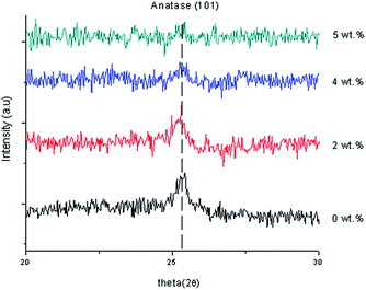
Fig. 2 reveals the XRD patterns of the TiO
2 nanoparticles, which show the apparent characteristic peaks of the anatase phase. The anatase nanocrystalline peak of 1 wt% Y doping concentration was measured at 25.2599° which corresponded to ICSD file no. 98-015-4601. The anatase peak of 4 wt% Y doping concentration was measured at 25.2065° which corresponded to ICSD file no. 98-000-9854 and the anatase nanocrystalline peak of 5 wt% Y doping concentration was measured at 25.2887° which corresponded to ICSD file no. 98-015-4602. No other phases were detected and at a larger than 5 wt% Y doping concentration indicated that they were amorphous in nature. Likewise, the intensity of the diffraction peaks decreased with increasing Y doping concentration in the TiO
2 lattice. This can be ascribed to Y impurities dislocating the crystal structure of the anatase TiO
2. This could be because some Ti
4+ was replaced by Y
3+ and by some Y
3+ entering into the TiO
2 lattice, or the yttrium(
III) oxide (Y
2O
3) content was an extremely small size and could not be detected. XRD patterns of pure and Y doped TiO
2 nanoparticles show that the characteristic peaks appear with wider FWHM and the intensity of the diffraction peaks decreased with an increase in the Y doping concentration. The ionic radius of Y
3+ was 0.088 nm, which was much larger than that of Ti
4+ at 0.074 nm, so as Y
3+ entered into the lattice of TiO
2, there was a lower diffraction intensity, and a wider diffraction peak and the crystal lattice changed, thus resulting in lower crystallinity. These results show that the appropriate Y doping concentration can maintain the crystallinity of TiO
2 nanoparticles. From the XRD analysis results, it was found that there were differences in the lattice constants between Y doped and pure TiO
2 thin film, which also inferred that Y
3+ entered into the lattice of TiO
2 and substitutes for the Ti
4+ ion which would eventually be beneficial for separating the charge carriers, extending their lifetime and effectively hindering the recombination of the electron–hole pairs.
17
 |
| | Fig. 2 XRD data of the undoped thin film and Y doped TiO2 thin film. | |
The position of 2θ was shifted to the left and the intensity decreased when the Y doping concentration increased because of the increase in the arrangement of the atoms. Furthermore, the FWHM became wider and the crystal size decreased because of the increase in the dislocation of the Al doping concentration. When a 1 wt% Y doping concentration was applied, the strain of the thin film increased, so the stress caused it to become a tensile thin film because of the positive sign. However, when a 4 wt% Y doping concentration was applied, the strain of the thin film increased, so the stress caused it to become a compressive thin film because of the negative sign.
The lattice constants of a and c were altered to a = 3.7970 and c = 9.5790 when 4 wt% Y doping concentration was applied as shown in Table 2. Doping Y atoms increased the lattice constant “a” of the tetragonal TiO2 structure, which may show that Y has entered into the TiO2 lattice. This shows that an increase in doping concentration weakens the film's crystallinity, which may be because of the stresses caused by the difference in ion size between titanium and the dopant and the segregation of dopants in the grain boundaries for high doping concentrations. The calculated crystallite sizes of Y doped TiO2 thin films with 1 wt%, 4 wt% and 5 wt% were 17.2 nm to 45.23 nm. A comparison of the (101) peaks between the undoped and Y doped TiO2 shows that the FWHM increased based on the doping concentrations.26
Table 2 Peak properties of Y doped TiO2 thin films at different doping concentrations
| Y doped TiO2 con. |
Position, 2 theta (°) |
Intensity (cts) |
FWHM (°) |
Calculated crystallite size, (D, nm) |
Dislocation (×1015) |
Strain |
Stress (GPa) |
Lattice constants |
| a |
c |
| 1 wt% |
25.2599 |
225.56 |
0.18 |
45.23 |
0.488 |
0.589 |
1.37 |
3.7960 |
9.4440 |
| 4 wt% |
25.2065 |
105.65 |
0.432 |
18.84 |
2.817 |
0.832 |
−1.94 |
3.7970 |
9.5790 |
| 5 wt% |
25.2887 |
131.65 |
0.4723 |
17.21 |
3.376 |
0.947 |
−0.221 |
3.7990 |
9.5090 |
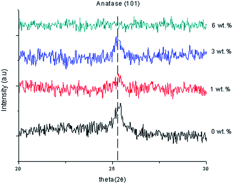
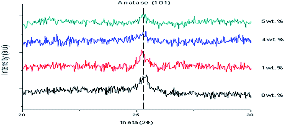
Fig. 3 shows XRD patterns of undoped and Gd doped TiO2 thin film using 2 wt%, 4 wt% and 5 wt% of Gd. The TiO2 indicated a dominant anatase phase for Gd-undoped sample. Then, no secondary phase was detected for Gd doped and undoped TiO2 thin films and more than 4 wt% Gd doping concentration indicated that they were amorphous in nature. The Gd dopant did not cause any shift in peak position of TiO2 which may be because the amount of Gd doping was too small. Gd doped TiO2 has smaller average size particles than the pure TiO2 as shown in Table 1. The diffraction peak of anatase indicated an offset to the lower angle region after doping Gd ions into the anatase TiO2 lattice and this demonstrated the incorporation of Gd3+ ions into TiO2 lattice by substituting them for the Ti4+ ion. The Gd3+ (with an ionic radius of 0.0938 nm) doping into Ti sites was challenging because of the large difference in the ionic radii. The results of the XRD studies left a lot of uncertainty about the content of crystalline and amorphous phases in the deposited thin films, and only verified that the modification of the chemical composition of deposited Gd doped TiO2 thin film really affects the growth mechanism, which has a direct impact on the microstructure.27
 |
| | Fig. 3 XRD data of the undoped thin film and Gd doped TiO2 thin film. | |
The anatase nanocrystalline peak of 2 wt% Gd doping concentration was measured at 25.2608° which corresponded to ICSD file no. 98-015-4601. The anatase peak of 4 wt% Gd doping concentration was measured at 25.3202° which corresponded to ICSD file no. 98-008-2084 and the anatase nanocrystalline peak of 5 wt% Gd doping concentration was measured at 25.2887° which corresponded to ICSD file no. 98-015-4601. Table 3 shows the lattice constants and crystallite size of the synthesized samples. The position of 2θ was shifted to the left and the intensity of the thin film decreased when the Gd doping concentration increased because of the increase in the arrangement the atoms. Furthermore, the FWHM became wider and the crystal size decreased because of the increase of the dislocation of the Gd doping concentration. When 1 wt% Gd doping concentration was applied, the strain of the thin film increased, so the stress created a tensile thin film because of the positive sign. When 4 wt% Gd doping concentration was applied, the strain of the thin film decreased, so the stressed thin film was still a tensile thin film. With 5 wt% Gd doping concentration, the strain value increased and the stressed thin film still remained as a tensile thin film. The lattice constants of a and c were changed to a = 3.7930 and c = 9.5090 when 4% Gd doping concentration was applied. However, doping with Gd atoms increased the lattice constant “a” of the tetragonal TiO2 structure, which may indicate that Gd had entered the TiO2 lattice. This suggested that an enlargement in the doping concentration reduces the crystallinity of the film and that this maybe because of stresses effected by the difference in ion radius size between titanium and the dopant, and the segregation of dopants in the grain boundaries for high doping concentrations. The calculated crystallite sizes of Gd doped TiO2 with 2 wt% and 4 wt% corresponded to 18.85 nm and 14.14 nm, respectively. Broadening of the crystallite was present and tended to decrease as a function of 2θ. A comparison of the (101) peaks between undoped and Gd doped TiO2 showed that the FWHM increased based on the doping concentrations. 28
Table 3 Peak properties of Gd doped TiO2 thin films at different doping concentrations
| Gd doped TiO2 con. |
Position, 2 theta (°) |
Intensity (cts) |
FWHM, (°) |
Calculated crystallite size, (D, nm) |
Dislocation (×1015) |
Strain |
Stress (GPa) |
Lattice constants |
| a |
c |
| 2 wt% |
25.2608 |
206.12 |
0.432 |
18.85 |
2.814 |
0.589 |
1.37 |
3.790 |
9.4440 |
| 4 wt% |
25.3202 |
96.9 |
0.576 |
14.14 |
5.002 |
0.032 |
0.07 |
3.7830 |
9.4970 |
| 5 wt% |
25.256 |
47.02 |
0.432 |
18.85 |
2.814 |
0.589 |
1.37 |
3.7960 |
9.4440 |
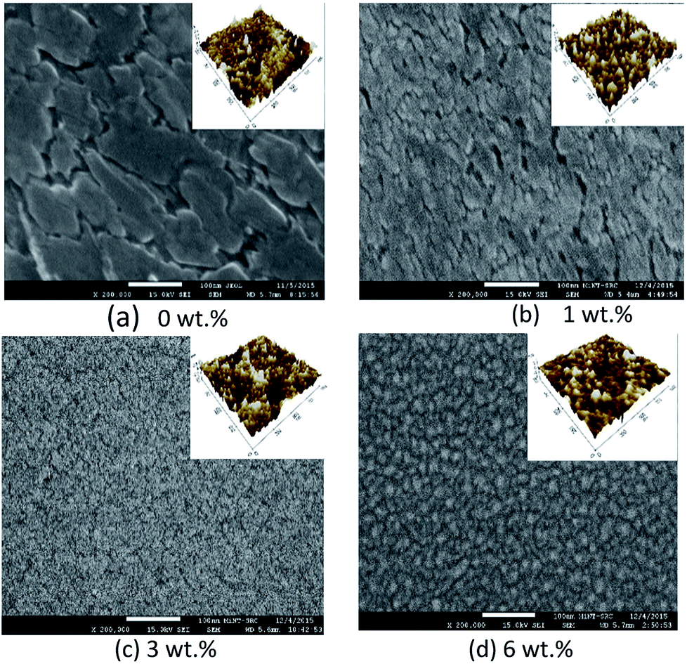
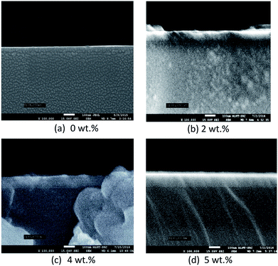
Fig. 4 and 5 show the surface morphology and cross-sectional area of an FESEM micrograph of pure and Al doped TiO2 thin films prepared using the sol–gel method. The Al doping concentrations, 1 wt%, 3 wt% and 6 wt% and their thicknesses are shown in Table 4. This shows the thickness, and verified the increase when the concentration of the Al doping increased. Al doped TiO2 thin films revealed the size of nanoparticles to be between 14 nm and 49 nm. The nanoparticle sizes decreased when the Al doping concentration process decreased, resulting in the nanoporous porosity. In order to determine the roughness of the surface as a function of the Al concentration, it was necessary to perform AFM. Fig. 4 depicts the two-dimensional AFM images of the deposited films using 1 wt%, 3 wt% and 6 wt% concentrations of Al doping. Table 4 shows that the grain size increased and the surface roughness of the Al–TiO2 thin film decreased. The lower roughness value showed that there was good homogeneity of the Al–TiO2 nanoparticles on the surface. The change in the grain shape was determined by analysing the XRD data. Based on the XRD data it can be seen that there is considerable variation in the maximum intensity peak, indicating the preferred growth direction of TiO2 for each phase formed with a decreasing Al doping concentration. The decomposition reaction kinetics at the substrate surface defined the grain shape and size. Larger grain sizes provided higher surface contact between the Al doped TiO2 thin films and the electrode thus improving electron migration.29
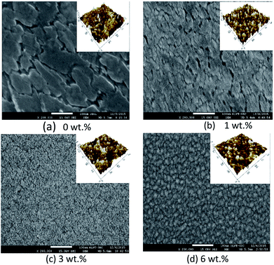 |
| | Fig. 4 Surface morphology of FESEM micrographs of pure and Al doped TiO2 thin films. | |
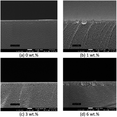 |
| | Fig. 5 Cross-sectional view of FESEM micrographs of pure and Al doped TiO2 thin films. | |
Table 4 Thickness, grain size and roughness with different Al doping concentration
| Al doping concentration |
Thickness (nm) |
Grain size (nm) |
Roughness (nm) |
| 0 wt% |
41.250 |
44.084 |
3.914 |
| 1 wt% |
55.313 |
69.000 |
0.792 |
| 3 wt% |
60.000 |
68.004 |
0.863 |
| 6 wt% |
75.937 |
103.00 |
0.487 |
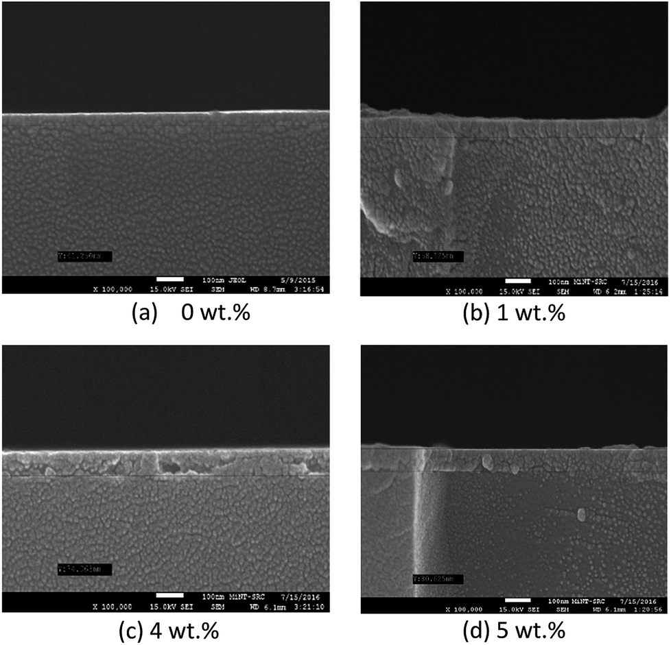
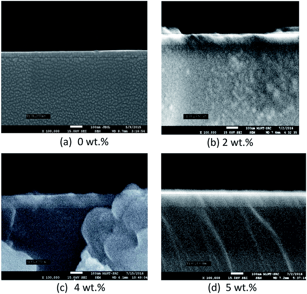
Fig. 6 and 7 show the surface morphology and the cross-sectional view of Y doped TiO2 thin films for all thin film samples. For samples deposited using a Y doping concentration, the thicknesses are shown in Table 5. This shows the increasing thickness that occur when the concentration of the Y doping increased. Morphological properties of the undoped and Y doped TiO2 thin films were examined using FESEM, and the images of the grainy looking structure became less grainy with Y doped in the TiO2 at 1 wt%, 4 wt% and 5 wt% concentrations. Nevertheless, the granules became smaller at 4 wt% doping concentration and the morphology shifted to a more uniform film structure. The AFM images of pure and Y doped TiO2 were prepared by using the spin coating method with yttrium(III) nitrate [Y(NO3)3] as a doping source as shown in Fig. 7. The Y doping had little influence on the morphology of the TiO2 thin film when the Y doping concentration was increased. It can be seen that the crystalline size of the nanoparticles was about 20 nm to 49 nm. The crystalline size of pure TiO2 nanoparticles was about 45.23 nm with a little agglomeration. With the increase in Y doping content, the crystalline size increased, and the agglomeration gradually increased when the Y doping content was at 1 wt%. The crystalline size of the nanoparticles increased to about 49 nm, and the agglomeration became more serious. This was mainly because of the sol–gel process, where the precursor of titanate reacted with NO3− and Ti(NO3)2 was obtained when the doped source Y(NO3)3 was added. Therefore, NO3− can also act as a chelating agent as well as a doping agent, both of which can slow down the condensation reaction rate, thus controlling the nucleation and growth process. Instead, the Y elements can strongly prevent the conversion of the TiO2 crystal phase. The AFM roughness analysis also shows the values of the roughness parameters.30
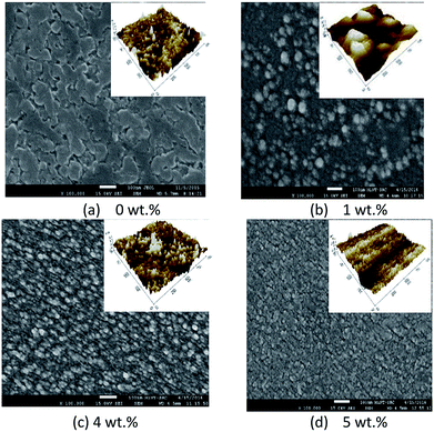 |
| | Fig. 6 Surface morphology of FESEM micrographs of pure and Y doped TiO2 thin films. | |
 |
| | Fig. 7 Cross-sectional view of FESEM micrographs of pure and Y doped TiO2 thin films. | |
Table 5 Thickness, grain size and roughness with different concentrations of Y doping
| Y doping con. |
Thickness (nm) |
Grain size (nm) |
Roughness (nm) |
| 0 wt% |
41.250 |
44.084 |
3.914 |
| 1 wt% |
58.125 |
40.760 |
13.925 |
| 4 wt% |
74.063 |
44.927 |
2.040 |
| 5 wt% |
80.625 |
63.000 |
0.979 |
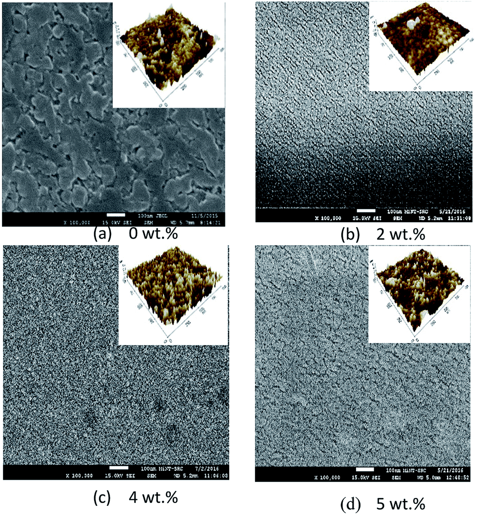
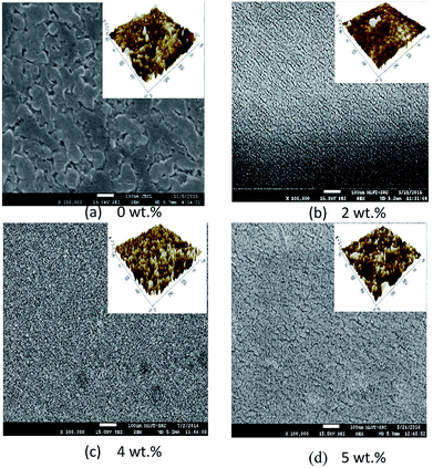
Fig. 8 and 9 show the surface morphology and cross-sectional view of Gd doped TiO2 thin films. The thicknesses are shown in Table 6. This shows the increasing thickness when the concentration of Gd doping was increased. Fig. 9 shows that the surface morphology of the Gd doping samples were nearly nanoparticles and had high porosity as the pure TiO2 and Gd doped nanoparticles became very small when an increase in the doping process was observed. Fig. 9 also reveals that the two-dimensional size was increased and as well there was an increase in roughness as shown in Table 6. The surface roughness determined the number of active surface sites. In addition, the lower roughness value indicated that the TiO2 particles had a very smooth surface. The AFM image shows that at 5 wt% Gd doping the thin film had the lowest roughness. The average grain sizes range around 40.760 nm to 63.000 nm. The changes in the grain shape were explained by examining the XRD data.28 When the AFM images of the deposited films were examined, it was found that as the Gd doping increased, then the grain size also increased and the roughness decreased. The thickness increased with increasing Gd doping concentration. It can be clearly observed from the results in Table 6 that the thickness is directly proportional to the Gd doping concentration.
 |
| | Fig. 8 FESEM micrographs showing the surface morphology of pure and Gd doped TiO2 thin films. | |
 |
| | Fig. 9 FESEM micrographs showing a cross-sectional view of pure and Gd doped TiO2 thin films. | |
Table 6 Thickness, grain size and roughness with different Gd doping concentrations
| Gd doping con. |
Thickness (nm) |
Grain size (nm) |
Roughness (nm) |
| 0 wt% |
41.250 |
44.084 |
3.914 |
| 2 wt% |
78.750 |
47.157 |
1.637 |
| 4 wt% |
95.625 |
63.190 |
0.759 |
| 5 wt% |
98.438 |
66.000 |
0.588 |
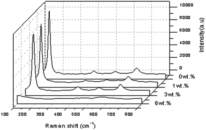
The Raman spectrum of the pure TiO2 at a spectral range of 100–800 cm−1 showed that four of the peaks were prominent and the corresponding modes at 144.913 cm−1 (Eg), 398.918 cm−1 (B1g), 517.139 cm−1 (a combination of A1g and B1g) and 636.698 cm−1 (Eg), were assigned to the anatase phase as shown in Fig. 10. The spectra of the doped TiO2 were slightly shifted as a result of the crystal structure modification from the doping. Raman spectroscopy was carried out to confirm the phase identification of the Al doped TiO2 thin films as well as to investigate the defects in the materials as shown in Fig. 9(a). The Eg mode of the pure TiO2 at 144.913 cm−1 arose from external vibrations of the anatase structure and indicated the formation of a long-range order, thus verifying the XRD data. Fig. 10 shows the room temperature Raman spectra of the Al doped TiO2, its Eg mode when 1 wt% of Al is used remains at 144.913 cm−1 but when a concentration of 3 wt% of Al is applied then a high intensity of Raman peak at 145.723 cm−1 was observed.
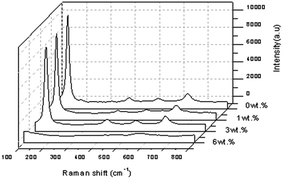 |
| | Fig. 10 Raman spectroscopy scans for Al doped TiO2 thin film. | |
The sharpest and strongest peak at about 145.723 cm−1 was assigned to the high frequency branch of the Eg mode of Al doped TiO2, which was the strongest mode in the anatase phase. The strong Eg mode indicated good crystallinity. Thus, from the Raman studies it was determined that the anatase phase was not altered by the presence of a trivalent aluminium dopant. It was noted that doping was considered to be the main factor that would cause the lattice distortion of the crystals, and this is usually due to the differences of the ionic radii of different elements. In this study, the crystallite quality of the Al doped TiO2 thin film with 3 wt% of Al was better than the crystallite quality of the other sample of TiO2 with a concentration of 1 wt% of Al doping.31 The crystallite quality of the doped TiO2 with 6% of Al was worse than with the other concentrations because no peak for the anatase phase of TiO2 was detected. Furthermore, FWHM showed pure TiO2 > Al doped TiO2 at the strongest peak, meaning that the FWHM decreased when the doping concentration increased.
Fig. 11 shows the Raman spectra of TiO2 with 1 wt%, 4 wt% and 5 wt% of Y concentration at a spectral range with high intensity Raman peaks of anatase TiO2 and no Raman peak for the rutile phase was noted. Four normal modes were observed at 144.913 cm−1 (Eg), 395.864 cm−1 (B1g), 517.139 cm−1 (a combination of A1g and B1g) and 636.698 cm−1 (Eg). The sharpest and strongest peak at about 144.913 cm−1 was assigned to the high frequency branch of the Eg modes of TiO2, which was the strongest mode in the anatase phase. The strongest Eg mode indicated good crystallinity as the Y doping concentration reached a concentration of 5 wt% of Y. Thus from the Raman studies it could be determined that the anatase phase was not changed by the presence of the trivalent yttrium dopant. It can also be observed that doping was considered to be the main factor that would cause the lattice distortion of the crystals, and this verified the XRD data, for it was generally different from the ionic radii of different elements.32 In this study, the crystallite quality of the Y doped TiO2 nanoparticles with 5 wt% of Y were better than the crystallite quality of the other sample of TiO2 with a doping concentration of 1 wt% and 4 wt% of Y. However, the value of the FWHM showed that pure TiO2 ≅ Y doped TiO2 at the strongest peak of 5 wt% doping, meaning that the FWHM rose slightly when the doping concentration was increased.17
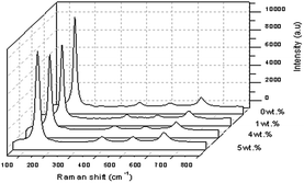 |
| | Fig. 11 Raman spectroscopy spectra for Y doped TiO2 thin film. | |
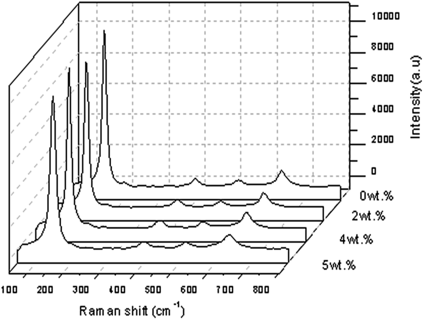
Fig. 12 shows the Raman spectra of the TiO2 with a Gd doping concentration of 2 wt%, 4 wt% and 5 wt% at a spectral range of 100–800 cm−1 with the highest intensity of Raman peaks of anatase TiO2 when a 4 wt% Gd doping concentration was applied. Four normal modes were observed at 144.913 cm−1 (Eg), 395.953 cm−1 (B1g), 514.128 cm−1 (a combination of A1g and B1g) and 636.698 cm−1 (Eg). The sharpest and strongest peak at about 144.913 cm−1 was assigned to the high frequency branch of the Eg mode of TiO2. This indicated good crystallinity. Thus, from the Raman studies it was determined that the anatase phase was not altered by the presence of a trivalent gadolinium dopant. The change in the position and shape of the Raman active Eg line of anatase TiO2 was also detected so that the doping concentration was thought to be the main aspect that could produce the lattice distortion of the crystals, which was normally different from the ionic radii of different elements. In this research, the crystallite quality of the Gd doped TiO2 with a doping concentration of 5 wt% of Gd was better than the crystallite quality of the other samples of TiO2 with 2 wt% and 4 wt% Gd doping concentrations. However, the value of FWHM showed Gd doped TiO2 < pure TiO2 at the strongest peak of 5 wt%, meaning that FWHM decreased slightly when the doping concentration increased.33
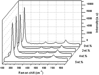 |
| | Fig. 12 Raman spectroscopy scan for Gd doped TiO2 thin film. | |
XPS was carried out to check the surface chemical composition, purity and the oxidation valence states of TiO2, and Al doped TiO2. In order to understand the mechanism resulting in the changes in the band gap of Al doped TiO2 films, the films were investigated using XPS. The XPS being a surface sensitive technique provided information about the change in the chemical state of the constituent species of film. Here, the variation in the chemical state of the O and Ti elements was determined in detail to correlate it to the observed variations in the band gap of the films.34
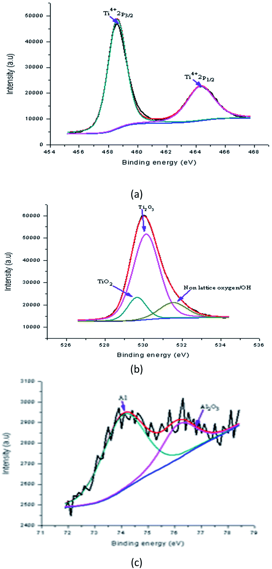
Fig. 13(a) shows a high resolution XPS spectrum of pure TiO2 film. In this spectrum, the doublet Ti2p3/2 (binding energy 458.20 eV) and Ti2p1/2 (binding energy 463.92 eV) occurs from the spin–orbit splitting. These peaks were consistent with Ti4+ in the TiO2 lattice. Next, the O1s spectrum of pure TiO2 thin film is shown in Fig. 13(b), which was fitted the three peaks. The peaks at binding energies of 529.65 eV, 531.85 eV and 534.50 eV were attributed to lattice oxygen, titanium(III) oxide (Ti2O3) and non-lattice oxygen, respectively.
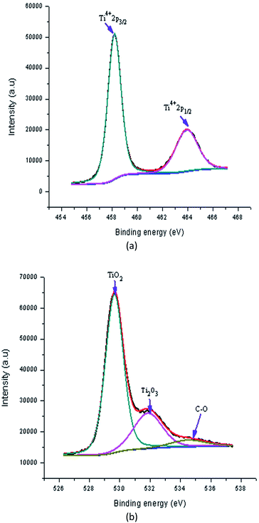 |
| | Fig. 13 High resolution XPS spectrum of pure TiO2 film (a) Ti2p and (b) O1s. | |
Fig. 14(a) shows the peaks in the Al doped samples now located at binding energies of 458.60 eV (Ti2p3/2) and 464.32 eV (Ti2p1/2). The sample was 3 wt% Al doped TiO2 thin films. The alteration in the position of these peaks shows the effect of an Al increase on the electronic state of the Ti element. It is most likely that some of the Ti ions are replaced with Al ions in the lattices. The rise in the area of the Ti4+ peak shows that either TiO2 was created in a large amount or some of the oxide structure mingled with the Al (having oxidation state Ti4+) which was created after the doping. Similarly, for the doped sample, the O1s spectrum of Al doped TiO2 thin film fitted with three peaks is shown in Fig. 14(b). In this spectrum, three peaks at binding energies of 529.65 eV, 530.13 eV and 531.52 eV were detected which were assigned to lattice oxygen, lattice oxygen (Ti2O3) and lattice oxygen (Ti2O3 + OH), respectively. This shows that in the doping process the TiO2 is created together with some mixed oxide.
 |
| | Fig. 14 High resolution XPS spectra of Al doped TiO2 film (a), Ti2p (b), O1s and (c) Al2p and Al2s. | |
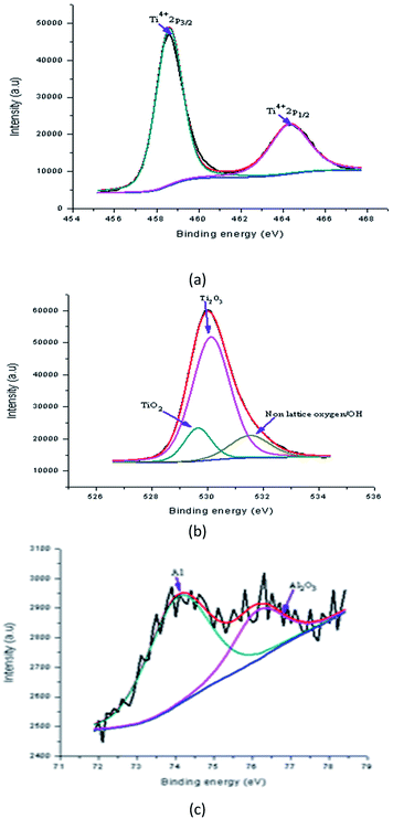
The alteration in stoichiometry was expected because of the change in area of the relative peaks. The Ti3+ state existed in the Al doped TiO2 in which the oxygen vacancy defects were created. Al doping results in a small alteration in the binding energy, revealing that the Al ions were better dispersed in the replacement sites of the TiO2 lattice and more mingled oxide structure, which could be Al–O–Ti. Fig. 14(c) shows the XPS spectrum at binding energies of 74.07 eV and 76.15 eV corresponding to the Al2p and Al2s of Al doped TiO2 film, respectively. The appearance of these peaks supports the existence of Al in the Al3+ ionic state.35
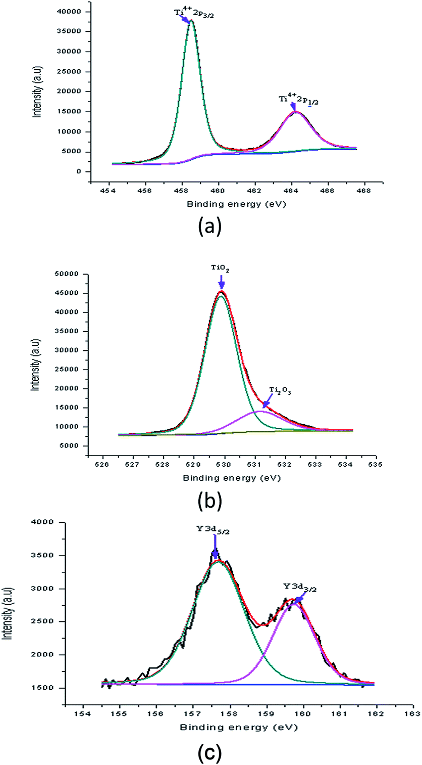
Fig. 15(a) shows the peaks in the Y doped samples that were detected at binding energies of 458.49 eV (Ti2p3/2) and 464.19 eV (Ti2p1/2). These peaks were assigned to 4 wt% Y doped TiO2. The shift in the position of these peaks shows the effect of a Y increase on the electronic state of the Ti element. Possibly some of the Ti ions were replaced with Y ions in the lattices. For the Y doped sample, the O1s spectrum of the Y doped TiO2 thin film fitted with three peaks is shown in Fig. 15(b). In this spectrum, two peaks at binding energies of 529.88 eV and 531.15 eV were observed which were assigned to lattice oxygen (TiO2) and Ti2O3, respectively. The Ti3+ state existed in the Y doped TiO2 in which oxygen vacancy defects were created. This showed that in the doping process TiO2 was created together with some mingled oxide. The alteration in stoichiometry was expected because of the change in area of the relative peaks. Nevertheless, the peak at a binding energy of 530.03 eV appeared to correspond to the lattice oxygen. The Y doping concentration results in a small alteration in the binding energy, showing that Y ions were better dispersed in the replacement sites of the TiO2 lattice and created a more mingled oxide structure, which could be Y–O–Ti. Fig. 15(c) shows the XPS spectrum at binding energies of 157.68 eV and 159.74 eV which corresponded to Y3d5/2 and Y3d3/2, respectively, of the Y doped TiO2 thin film. The creation of these peaks preserved the existence of Y in the Y3+ ionic state. These peaks also show that the usual Y3d spectra with spin-doublets (d3/2 and d5/2) were separated by two peaks, both of 2.06 eV.36
 |
| | Fig. 15 High resolution XPS spectrum of Y doped TiO2 film (a) Ti2p, (b) O1s, and (c) Y3d. | |
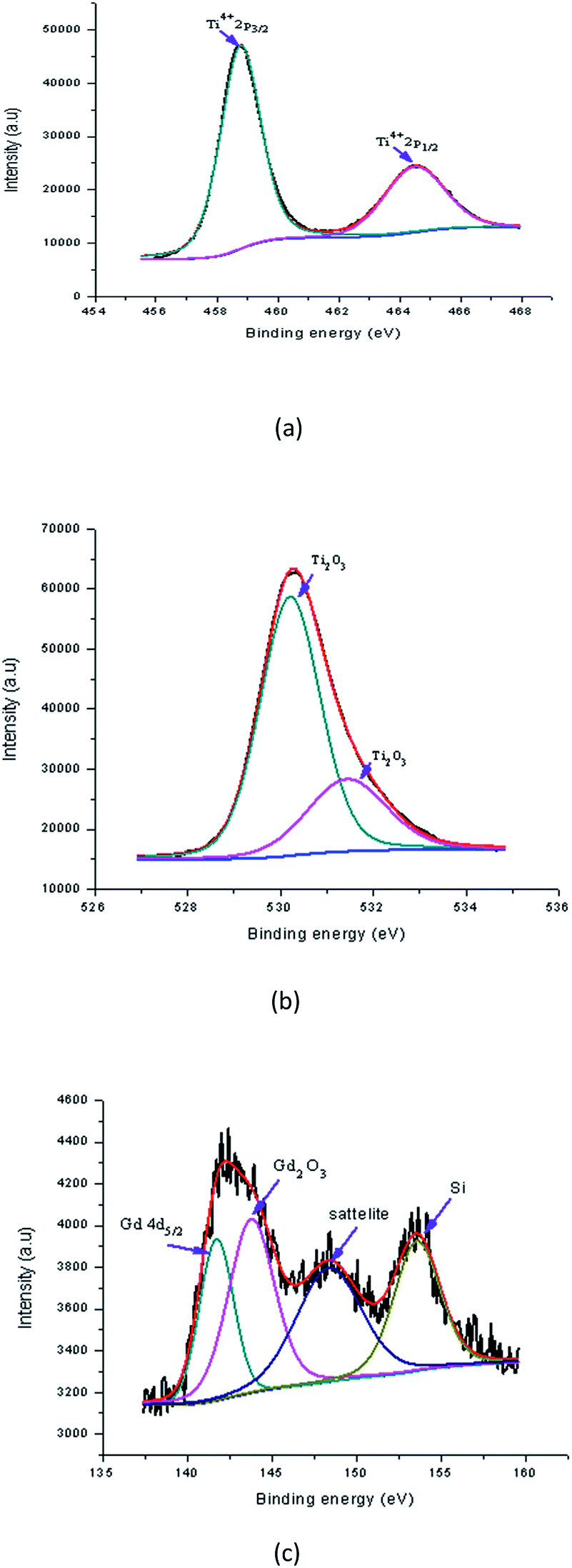
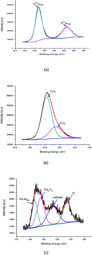
Fig. 16(a) shows the peaks in the Gd doped samples that were found at binding energies of 458.77 eV (Ti2p3/2) and 464.49 eV (Ti2p1/2). The alteration in the position of these peaks shows the effect of Gd accumulation on the electronic state of the Ti element. Possibly some of the Ti ions were replaced with Gd ions in the lattices. The area of the Ti4+ peak shows that either TiO2 was created in a large amount or some mingled oxide structure with Gd (having the oxidation state of Ti4+) was created after doping. Meanwhile, the reducing area of the Ti4+ indicated a reduction of TiO2 in the sample, and probably the creation of the Ti–O–Gd structure in the TiO2 lattice through the replacement of transition metal ions. The detected alteration in the peaks also showed contact between the Ti and Gd atoms and an overlapping of their 4d orbital. Fig. 16(b) shows the Gd doped sample, in which the O1s spectrum of the Gd doped TiO2 thin film was fitted with two peaks that were detected at binding energies of 530.21 eV and 531.43 eV which were assigned to lattice oxygen (Ti2O3) and lattice oxygen (Ti2O3), respectively. The Ti3+ state existed in the Y doped TiO2 in which the oxygen vacancy defects were created. This showed that defects in the doping process of TiO2 were created together with some mingled oxide. The alteration in stoichiometry was expected because of the alteration in the area of the relative peaks. Nevertheless, the TiO2 peak at the binding energy 529.91 eV appeared to correspond to the lattice energy. Fig. 16(c) revealed that the Gd ions were better dispersed in the replacement sites of the TiO2 lattice and created a more mingled oxide structure, which could be Gd–O–Ti. This also showed that the XPS spectrum at binding energies of 141.73 eV and 143.79 eV corresponded to Gd4d5/2 and gadolinium(III) oxide (Gd2O3) of the Gd doped TiO2 film, respectively. The creation of these peaks encouraged the existence of Gd in the Gd3+ ionic state. A shake up satellite peak at 148 eV also encouraged Gd to be exhibited in the Gd3+ state as an oxide. These shake-up satellite peaks were related to the Gd3d–O2p hybridisation. Thus, the XPS analysis indicated that Gd ions were doped into the TiO2 matrix in the form of Gd–O–Ti.37
 |
| | Fig. 16 High resolution XPS spectra of Gd doped TiO2 film (a) Ti2p, (b) O1s, and (c) Gd4d. | |
Conclusions
Pure titanium dioxide (TiO2) and doped TiO2 thin films were prepared by spin coating titanium(IV) butoxide on a glass substrate from a sol–gel, followed by annealing at 500 °C. The anatase phase was observed to be annealed at 500 °C. The doped TiO2 thin film was produced by doping with metal atoms for which the ionic state was a 3+ ion, which were Al, Gd, and Y. The ionic state, 3+, of the metal atom doping based on lattice distortion could contribute oxygen vacancy defects that provided advantages to the thin film. The conductivity increase because of a faster growth of the thin film encouraged the formation of a higher level of oxygen vacancy defects. These thin films can be applied in gas sensor applications.
Conflicts of interest
There are no conflicts of interest to declare.
Acknowledgements
The authors would like to acknowledgment the Ministry of Education Malaysia for financial support from the Fundamental Research Grant Scheme (FRGS) Grant vot 1507, IGSP U675 Universiti Tun Hussein Onn Malaysia (UTHM), CREST Fund A154 and UTHM for the technical facilities.
Notes and references
- S. Boyadjiev, et al., Gas sensing properties of very thin TiO2 films prepared by atomic layer deposition (ALD), J. Phys.: Conf. Ser., 2014, 559, 12013 CrossRef.
- A. A. Haidry, et al., Characterization and hydrogen gas sensing properties of TiO2 thin films prepared by sol–gel method, Appl. Surf. Sci., 2012, 259, 270–275 CrossRef.
- Y. Lan, Y. Lu and Z. Ren, Mini review on photocatalysis of titanium dioxide nanoparticles and their solar applications, Nano Energy, 2013, 2, 1031–1045 CrossRef.
- J. A. Byrne, et al., Titanium Dioxide Nanostructured Coatings: Application in Photocatalysis and Sensors, 2006, vol. 1, pp. 72–75 Search PubMed.
- M. Akimoto, T. Toyoda, T. Okuno, S. Hayase and Q. Shen, Effect of defects in TiO2 nanotube thin film on the photovoltaic properties of quantum dot-sensitized solar cells, Thin Solid Films, 2015, 590, 90–97 CrossRef.
- D. Mahesh and J. Rajesh, TiO2 Microstructure, Fabrication of thin Film Solar Cells and Introduction to Dye Sensitized Solar Cells, Res. J. Recent Sci., 2003, 2, 25–29 Search PubMed.
- T. Xie, et al., The effects of surface conditions of TiO2 thin fi lm on the UV assisted sensing response at room temperature, Thin Solid Films, 2006, 620, 76–81 CrossRef.
- A. Di Paola, S. Ikeda, G. Marcì, B. Ohtani and L. Palmisano, Transition metal doped TiO2: physical properties and photocatalytic behaviour, Int. J. Photoenergy, 2001, 3, 171–176 CrossRef.
- L. B. Xiong, J. L. Li, B. Yang and Y. Ying, Ti3+ in the surface of titanium dioxide: generation, properties and photocatalytic application, J. Nanomater., 2012, 1–13 Search PubMed.
- K. M. Prabu and P. M. Anbarasan, Preparation and Characterization of Aluminium Doped Titanium Dioxide Nanoparticles by Sol-Gel Method for Solar Cell Applications, Int. J. Sci. Res. Dev., 2014, 2, 560–564 Search PubMed.
- B. Bharti, S. Kumar, H. Lee and R. Kumar, Formation of oxygen vacancies and Ti3+ state in TiO2 thin film and enhanced optical properties by air plasma treatment, Sci. Rep., 2016, 6, 32355 CrossRef PubMed.
- G. Yang, T. Wang, B. Yang, Z. Yan and S. Ding, Applied Surface Science Enhanced visible-light activity of F-N co-doped TiO2 nanocrystals via nonmetal impurity, Ti3+ ions and oxygen vacancies, Appl. Surf. Sci., 2013, 287, 135–142 CrossRef.
- R. K. Sharma, et al., Influence of doping on sensitivity and response time of TiO2 oxygen gas sensor, Rev. Sci. Instrum., 2014, 1500 Search PubMed.
- C. Wu, Y. Lee, Y. Lo, C. Lin and C. Wu, Applied Surface Science Thickness-dependent photocatalytic performance of nanocrystalline TiO2 thin films prepared by sol–gel spin coating, Appl. Surf. Sci., 2013, 280, 737–744 CrossRef.
- A. Xu, Y. Gao and H. Liu, The Preparation, Characterization, and their Photocatalytic Activities of Rare-Earth-Doped TiO2 Nanoparticles, J. Catal., 2002, 157, 151–157 CrossRef.
- S. Cornelius, Charge transport limits and electrical dopant activation in transparent conductive (Al, Ga): ZnO and Nb: TiO2 thin films prepared by reactive magnetron sputtering, PhD thesis, Technische Universitat Dresden, 2014, p. 225.
- W. Zhang, K. Wang, S. Zhu, Y. Li, F. Wang and H. He, Yttrium-doped TiO2 films prepared by means of DC reactive magnetron sputtering, Chem. Eng. J., 2009, 155, 83–87 CrossRef; X. Pei, J. Chen and H. He, Effects of Al doping on properties of xAl–3%In–TiO2 photocatalyst prepared by a sol–gel method, Mater. Sci. Semicond. Process., 2015, 38, 24–30 CrossRef.
- M. Z. Atashbar, H. T. Sun, B. Gong, W. Wlodarski and R. Lamb, XPS study of Nb-doped oxygen sensing TiO2 thin films prepared by sol-gel method, Thin Solid Films, 1998, 326, 238–244 CrossRef.
- M. Zalas, Gadolinium-modified titanium oxide materials for photoenergy applications: a review, J. Rare Earths, 2014, 32, 487–495 CrossRef.
- W. Zhang, X. Pei, J. Chen and H. He, Effects of Al doping on properties of xAl–3%In–TiO2 photocatalyst prepared by a sol–gel method, Mater. Sci. Semicond. Process., 2015, 38, 24–30 CrossRef.
- N. D. M. Said, M. Z. Sahdan, I. Senain, A. S. Bakri, S. A. Abdullah, F. Mokhter, A. Ahmad and H. Saim, Effects of annealing temperature on structural, morphology and optical properties of TiO2 thin film, ARPN J. Eng. Appl. Sci., 2016, 11, 1819–6608 Search PubMed.
- L. B. Freund and S. Suresh, Thin Film Materials: Stress, Defect Formation and Surface Evolution, Cambridge University Press, 2004 Search PubMed.
- S. Miyazaki and R. L. Sachdeva, Shape memory effect and superelasticity in Ti–Ni alloys, in Shape Memory Alloys for Biomedical Applications, ed. T. Yoneyama and S. Miyazaki, Woodhead Publishing, 2009, ch. 1, pp. 3–19, DOI:10.1533/9781845695248.1.3.
- C. Paper, et al., Effects of Al doping on structural, morphology, electrical and optical properties of TiO2 thin film, 2017, DOI:10.1063/1.4968383.
- J. Choi, H. Park and M. R. Hoffmann, Effects of Single Metal-Ion Doping on the Visible-Light Photoreactivity of TiO2, J. Phys. Chem. C, 2010, 114, 783–792 CrossRef.
- K. Siva, et al., Phase control of yttrium (Y)-doped TiO2 nanofibers and intensive visible photoluminescence, J. Alloys Compd., 2014, 617, 683–687 CrossRef.
- M. Saif, et al., Nanostructured Gd3+-TiO2 surfaces for self-cleaning application, J. Mol. Struct., 2014, 1067, 120–126 CrossRef.
- J. Xu, Y. Ao, D. Fu and C. Yuan, Synthesis of Gd-doped TiO2 nanoparticles under mild condition and their photocatalytic activity, Colloids Surf., A, 2009, 334, 107–111 CrossRef.
- M. Z. Musa, et al., Aluminium doping of titanium dioxide thin films using sol–gel method, Mater. Res. Innovations, 2011, 15, s137–s140 CrossRef.
- N. I. U. Xinshu, L. I. Sujuan, C. Huihui and Z. Jianguo, Preparation, characterization of Y3+-doped TiO2 nanoparticles and their photocatalytic activities for methyl orange degradation, J. Rare Earths, 2011, 29, 225–229 CrossRef.
- A. Arunachalam, S. Dhanapandian and C. Manoharan, Effect of Sn doping on the structural, optical and electrical properties of TiO2 films prepared by spray pyrolysis, Phys. E, 2016, 76, 35–46 CrossRef.
- Z. K. Heiba and L. Arda, XRD, XPS, optical, and Raman investigations of structural changes of nano Co-doped ZnO, J. Mol. Struct., 2012, 1022, 167–171 CrossRef.
- G. A. Botton, et al., Electron energy loss spectroscopy of interfacial layer formation in Gd2O3 films deposited directly on Si(001), J. Appl. Phys., 2002, 91, 2921–2928 CrossRef.
- X. Q. Cheng, et al., Structural, morphological, optical and photocatalytic properties of Gd-doped TiO2 films, Thin Solid Films, 2016, 615, 13–18 CrossRef.
- R. Valaski, et al., Enhancement of open-circuit voltage on organic photovoltaic devices by Al-doped TiO2 modifying layer produced by sol–gel method, Thin Solid Films, 2014, 572, 2–7 CrossRef.
- X. Qu, et al., Results in Physics Yttrium doped TiO2 porous film photoanode for dye-sensitized solar cells with enhanced photovoltaic performance, Results Phys., 2016, 6, 1051–1058 CrossRef.
- S. Paul, B. Choudhury and A. Choudhury, Magnetic property study of Gd doped TiO2 nanoparticles, J. Alloys Compd., 2014, 601, 201–206 CrossRef.
|
| This journal is © The Royal Society of Chemistry 2018 |
Click here to see how this site uses Cookies. View our privacy policy here. 
 Open Access Article
 This Open Access Article is licensed under a
  *ab,
Mohd Zainizan Sahdana,
Nafarizal Nayan
*ab,
Mohd Zainizan Sahdana,
Nafarizal Nayan