
 Open Access Article
 This Open Access Article is licensed under a Creative Commons Attribution-Non Commercial 3.0 Unported Licence
Investigations on the bias temperature stabilities of oxide thin film transistors using In–Ga–Zn–O channels prepared by atomic layer deposition
So-Jung Yoon a,
Nak-Jin Seongb,
Kyujeong Choib,
Woong-Chul Shinb and
Sung-Min Yoon*a
a,
Nak-Jin Seongb,
Kyujeong Choib,
Woong-Chul Shinb and
Sung-Min Yoon*a
aDepartment of Advanced Materials Engineering for Information and Electronics, Kyung Hee University, Yongin, Gyeonggi-do 17104, Korea. E-mail: sungmin@khu.ac.kr
bNCD Co. Ltd, Daejeon 34015, Korea
First published on 11th July 2018
Abstract
Bias temperature stress stabilities of thin-film transistors (TFTs) using In–Ga–Zn–O (IGZO) channels prepared by the atomic layer deposition process were investigated with varying channel thicknesses (10 and 6 nm). Even when the IGZO channel thickness was reduced to 6 nm, the device exhibited good characteristics with a high saturation mobility of 15.1 cm2 V−1 s−1 and low sub-threshold swing of 0.12 V dec−1. Excellent positive and negative bias stress stabilities were also obtained. When positive bias temperature stress (PBTS) stability was tested from 40 to 80 °C for 104 s, the threshold voltages (VTH) of the device using the 6 nm-thick IGZO channel shifted negatively, and the VTH shifts increased from −0.5 to −6.9 V with the increasing temperature. Time-dependent PBTS instabilities could be explained by a stretched-exponential equation, representing a charge-trapping mechanism.
Introduction
Amorphous In–Ga–Zn–O (a-IGZO) thin films are the most promising channel materials for oxide semiconductor thin-film transistors (TFTs), which have drawn attention due to their high mobility and optical transparency.1–3 For the next-generation displays employing oxide TFT back-planes, the method used for the deposition of the a-IGZO thin films can be a critical factor governing the performance parameters such as higher resolution, large-area uniformity, and better device stability with a higher degree of form factor including ultra-thin and flexible structures.4,5 Atomic layer deposition (ALD) has recently been reported as a replacement for the conventional sputtering method for fabricating a-IGZO thin films.6,7 Radio-frequency magnetron sputtering has been the backbone for developing a-IGZO back-plane devices during the recent mass production of active-matrix organic light emitting diode (AMOLED) displays, but plausible plasma damages and high-temperature post-annealing processes may deteriorate the process margins from achieving higher performance and wider application fields. Furthermore, since ALD is dominated by a self-limiting growth mechanism, film thickness and composition can be precisely controlled even on large-area substrates, and its good step coverage with excellent film conformity can be extremely beneficial in various applications.8–10 To exploit the advantages of these remarkable features of the ALD process, various oxide semiconductors, such as ZnO,11–13 In–O,14 In–Zn–O,6 and Zn–Sn–O,15 have been prepared by the ALD process for TFT applications. TFTs with ALD-grown ZnO channels have been extensively investigated during the early developmental stages of oxide TFTs. However, they have exhibited critical disadvantages in securing device uniformities owing to the poly-crystalline natures of the ALD ZnO thin films. Furthermore, the device shows low mobility and poor bias-temperature stress instability. Alternatively, even with other amorphous oxide compositions prepared by the ALD process, high performance and robust stability cannot be guaranteed at the same time. Meanwhile, a-IGZO is regarded as the most well-designed composition for device applications. Thus, if we can prepare the a-IGZO films by ALD while keeping the material benefits of a-IGZO, it can provide a possibility to extend the applications of IGZO-TFTs due to the advantages of the ALD process.We have previously reported the device characteristics of ALD-grown IGZO-TFTs and their temperature dependence during the ALD process.7 When a-IGZO was prepared at an ALD temperature of 150 °C, the device exhibited good characteristics including a carrier mobility of 10.4 cm2 V−1 s−1 at the saturation region and robust stability. This could be significant in developing ALD as a promising deposition method for a-IGZO thin films. To thoroughly exploit the merits of the ALD process, it is important to investigate the device stabilities of the fabricated TFTs. While several studies have been carried out on sputter-deposited IGZO TFTs against bias and illumination stresses,16–19 limited information is available on the device stabilities when the active channel of a-IGZO is prepared by the ALD process.
Thus, the main objective of this study is to carefully evaluate the device stabilities of TFTs using a-IGZO channels prepared by ALD under positive-bias stress (PBS), negative-bias stress (NBS), and positive-bias-temperature stress (PBTS). We fabricated top-gate TFTs using the a-IGZO channels, and their film thicknesses were varied to 10 and 6 nm to verify the channel thickness dependence. In addition, the PBTS instabilities of these devices were also compared with those of TFTs using sputter-deposited IGZO channels. This study provides guidelines on the reliability of devices using ALD IGZO TFTs, as they are critical for practical applications.
Experimental section
Top-gate ALD-IGZO TFTs were fabricated on 150 nm-thick indium-tin oxide (ITO) source/drain (S/D)-patterned glass substrates. The IGZO channel layers were prepared by ALD process, in which the deposition temperature was fixed at 150 °C. To investigate the dependence of channel thickness on device stabilities, IGZO film thicknesses were varied to 10 and 6 nm by controlling the number of ALD super-cycles to 50 and 30, respectively. Indium-gallium single precursor, diethyl zinc (DEZ), and ozone (O3) were chosen as the precursors for In–Ga, Zn, and oxygen, respectively. The atomic ratio of In![[thin space (1/6-em)]](https://www.rsc.org/images/entities/char_2009.gif) :Ga:Zn in the IGZO film was found to be approximately 1:1:3. A 9 nm-thick Al2O3 layer was successively deposited as a protective layer at 150 °C by the ALD process using trimethylaluminum (TMA) and water vapor (H2O) as Al and oxygen sources, respectively. The protective and the IGZO channel layers were patterned using a diluted hydrofluoric acid-based (DHF) wet etchant. Then, a 100 nm-thick Al2O3 layer as a gate insulator was also deposited at 150 °C using ALD. Finally, the gate electrodes and S/D pads were patterned by a lift-off process with a 150 nm-thick ITO layer deposited at room temperature by DC sputtering. A post-annealing process was carried out for all the fabricated IGZO TFTs at 180 °C for 1 hour in the presence of oxygen. Fig. 1(a)–(c) show the schematic cross-sectional diagram, a microscopic image of the fabricated top-gate TFT, and a photograph of the transparent device fabricated on a glass substrate, respectively.
:Ga:Zn in the IGZO film was found to be approximately 1:1:3. A 9 nm-thick Al2O3 layer was successively deposited as a protective layer at 150 °C by the ALD process using trimethylaluminum (TMA) and water vapor (H2O) as Al and oxygen sources, respectively. The protective and the IGZO channel layers were patterned using a diluted hydrofluoric acid-based (DHF) wet etchant. Then, a 100 nm-thick Al2O3 layer as a gate insulator was also deposited at 150 °C using ALD. Finally, the gate electrodes and S/D pads were patterned by a lift-off process with a 150 nm-thick ITO layer deposited at room temperature by DC sputtering. A post-annealing process was carried out for all the fabricated IGZO TFTs at 180 °C for 1 hour in the presence of oxygen. Fig. 1(a)–(c) show the schematic cross-sectional diagram, a microscopic image of the fabricated top-gate TFT, and a photograph of the transparent device fabricated on a glass substrate, respectively.
 | ||
| Fig. 1 (a) Schematic cross-sectional view and (b) microscopic image of the fabricated device. (c) Photo image of the transparent IGZO TFT. | ||
The electrical characteristics of the fabricated IGZO TFTs were evaluated using a semiconductor parameter analyzer (Keithley 4200SCS) in a dark box at room temperature (RT). The channel width (W) and length (L) of the evaluated TFTs were 40 and 20 μm, respectively. The PBTS tests for the devices were carried out using a vacuum chamber probe station (M5VC, MS-Tech) equipped with hot chuck from RT to 80 °C in air. The electrical conductivity of ALD-grown IGZO films was measured by a four-point probe with temperature changes in the range from 50 to 250 °C.
Results and discussions
The electronic natures of the ALD-grown IGZO thin films were initially investigated before the evaluation on the device characteristics. To examine the temperature-dependent electrical properties and the IGZO channel thickness dependences, the variations in electrical conductivities (σc) were calculated from the obtained sheet resistance (Rs) values, as shown in Fig. 2. IGZO films were prepared by insulating SiO2/Si substrates for in situ four-point probe measurements. The measurement temperature was altered from 50 to 250 °C in both forward and reverse directions, and the ramping rate was set at 5 °C min. The initial values of σc for both films were approximately 10−9 S cm−1 and did not show any remarkable differences until the measurement temperature approached 95 °C. In this temperature range, the IGZO films showed near-insulating characteristics, and carriers were not transported by electronic conduction. Noticeably, both films showed dramatic changes in σc at particular temperatures, which were estimated to be approximately 96 and 126 °C for the IGZO thin films with thicknesses of 10 and 6 nm, respectively. Above these temperatures, the σc values of both films increased with the increasing temperature, which suggested that the IGZO films showed typical semiconducting carrier transport behaviors.20,21 Then, marked variations in σc between the films disappeared above 190 °C, and the σc values were almost constant for both the films when the measurement temperature returned to RT. To further discuss these results, we calculated the activation energies (EA) for the conduction behaviors using the Arrhenius equation. The values of EA obtained from the temperature-dependent conduction regions during the forward temperature sweeps were calculated to be approximately 1.85 and 4.90 eV for the IGZO films with thicknesses of 10 and 6 nm, respectively. A larger value of EA means that higher energy will be required to activate the conduction carriers. It was found that the σc values obtained when the temperature finally rose to 250 °C increased with the increasing IGZO thickness. The high σc value of the film could be closely related to the large quantity of defect-assisted conduction carriers within the film. Thus, the IGZO channel thickness can be expected to influence TFT characteristics such as conduction carrier mobility and device stability of ALD-IGZO TFTs. | ||
| Fig. 2 Variations in in situ temperature-dependent electrical conductivities for the ALD-grown IGZO films with different film thicknesses in an Arrhenius plot. The substrate temperature was swept in the range from 50 to 250 °C with a ramping rate of 5 °C min. | ||
Fig. 3(a) shows drain current (IDS) – gate voltage (VGS) characteristics and gate leakage currents (IGS) of the fabricated TFTs having different thickness of 10 and 6 nm using ALD-IGZO channels. VGS was increased from −20 to 20 V in both forward and reverse directions, and the drain voltages (VDS) were set as 0.5 and 5.5 V. Both TFTs showed excellent transfer characteristics without hysteresis behaviors. For the 10 nm-thick IGZO device, the carrier mobility at the saturation region (μsat) and subthreshold swing (SS) were measured to be 14.2 cm2 V−1 s−1 and 0.18 V dec−1, respectively; the same device parameters for the 6 nm-thick IGZO device were found to be 15.1 cm2 V−1 s−1 and 0.12 V dec−1, respectively. These results suggested that ALD-IGZO TFTs exhibited good performances with high μsat and low SS. The transfer characteristics of ALD IGZO TFTs also showed excellent device-to-device uniformity and reproducibility. The averages and standard deviations of VTH and μsat of the 6 nm-thick IGZO TFTs were 2.57 ± 0.44 V and 15.1 ± 0.53 cm2 V−1 s−1, respectively. Fig. 3(b) shows IDS – VDS output characteristics of the 6 nm-thick IGZO TFTs. VDS was swept from 0 to 10 V at various VGS conditions of −3, 0, 3, 6, and 9 V, and TFTs exhibited good ohmic behaviors in the linear regions without current crowding. Furthermore, excellent gate-bias modulation of the drain current and hard saturation operations could also be observed in the saturation regions. The obtained values for IDS were consistent with those estimated for the transfer characteristics of IGZO TFTs.
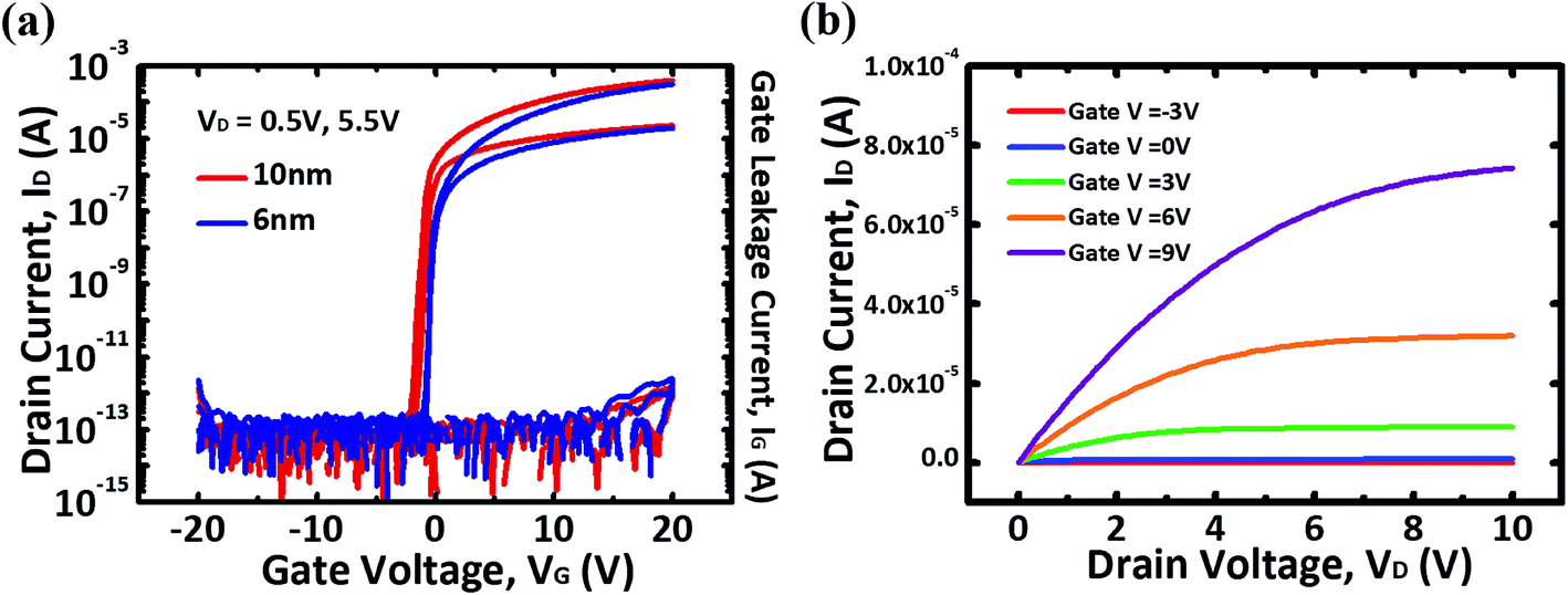 | ||
| Fig. 3 (a) Comparisons of the IDS–VGS transfer characteristics and IGS gate leakage currents between the devices using ALD IGZO channels with thicknesses of 6 and 10 nm. (b) IDS–VDS output characteristics for the TFT using 6 nm-thick IGZO channel. | ||
Prior to the evaluations of the device stabilities, we investigated and compared the trap densities in the channel mid-gap regions for the devices using ALD IGZO channels with different thicknesses. The transfer characteristics of both TFTs were measured with the variations in measurement temperatures from 298 to 373 K, as shown in Fig. 4(a) and (b). The VTH values of oxide TFTs generally shift negatively with the increasing temperature because of thermally activated free electrons from the band gap of the channel. The conducting free electrons may originate from the electron transitions within the band gap and the generation of oxygen vacancies. Thermally activated free electrons may be transferred from shallow and/or deep trap sites to beneath the conduction band. Furthermore, more free electrons can be generated along with oxygen vacancies induced by thermal excitation.22,23 The temperature-dependent VTH shifts of ALD-IGZO TFTs were examined to be only −1.0 and −1.2 V when the IGZO channel thicknesses were varied to 10 and 6 nm, respectively. The SS values slightly increased with the increasing temperature, whereas there was no marked change in the μsat values. To estimate the differences in the density of states within the channels for both TFTs, the EA values for the VTH shifts in the subthreshold region and their decreasing rates were calculated as a function of gate voltage from the Arrhenius plot using eqn (1), as shown in Fig. 4(c).
 | (1) |
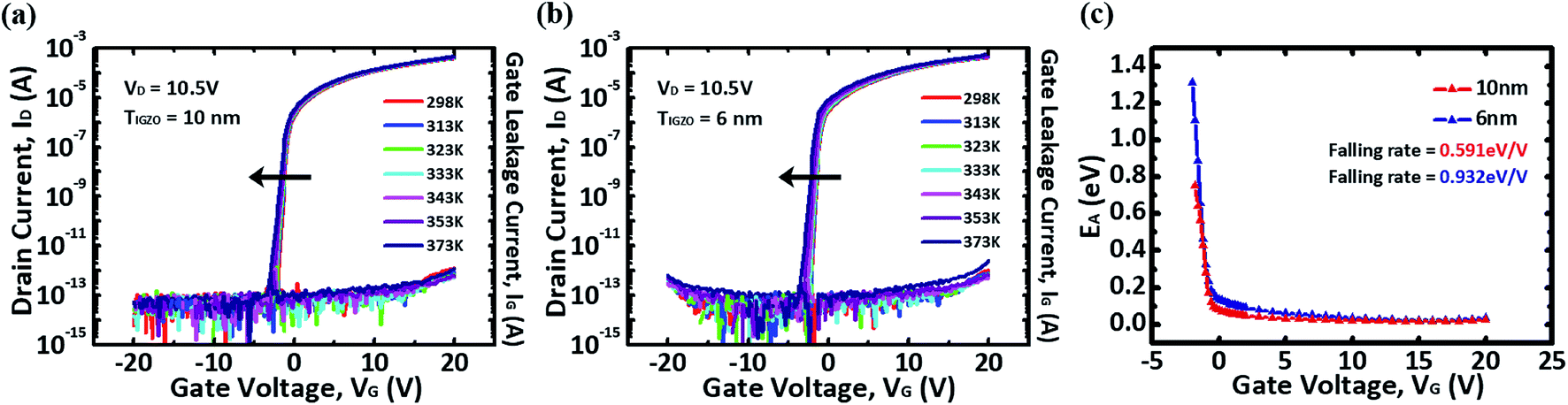 | ||
| Fig. 4 Changes in the transfer characteristics with different channel thickness of the (a) 10 nm-thick and (b) 6 nm-thick IGZO TFTs with measurement temperature variations from 298 to 373 K. (c) Variations in activation energy as a function of VGS for the IGZO TFTs with different IGZO channel thicknesses of 10 and 6 nm. | ||
Consequently, even when the IGZO channel thickness was reduced to 6 nm, the overall device characteristics could be enhanced compared to those of the device with 10 nm-thick channel. Thus, the operation stabilities of the devices fabricated with 6 nm-thick a-IGZO channels were preferably evaluated for gate bias and temperature stresses. Fig. 5(a) and (b) show the positive and negative gate bias stress (PBS and NBS) stabilities when a voltage of +20 or −20 V was continuously applied to the gate terminal for 104 s. The shift of VTH (ΔVTH) was measured to be −0.1 V under PBS, and there were no marked variations in ΔVTH under NBS. As can be seen in these figures, ALD-IGZO TFTs were well-fabricated and exhibited excellent PBS and NBS characteristics without degradation of SS values, which indicated that the devices exhibited good interface properties without developing additional defects during the stress tests.19 PBTS instabilities were investigated for the same devices. Fig. 5(c)–(e) show the variations in the transfer curves under PBTS at various temperatures of 40, 60, and 80 °C, respectively. In these tests, the VGS and VDS biases were set as +20 and 10.5 V, respectively. Generally, the positive shift of VTH under PBTS conditions is explained by the electron trapping mechanism within GI and/or at the interface between the GI and IGZO channel layers.26,27 However, ΔVTH values for TFTs using ALD IGZO channels were measured as −0.5, −1.8, and −6.9 V in the PBTS tests at temperatures of 40, 60, and 80 °C, respectively. There were no marked variations in the PBTS instabilities in the linear region of IDS (VDS = 0.5 V). The ΔVTH values increased with the increasing PBTS temperature; the obtained values were comparable with those of previously reported devices mainly fabricated with sputtered IGZO channels.18,28
 | ||
| Fig. 5 Variations in IDS–VGS curves for the TFT using 6 nm-thick IGZO channel with the time evolution under (a) PBS, (b) NBS, PBTS at (c) 40, (d) 60, and (e) 80 °C. | ||
Furthermore, the PBTS characteristics of IGZO TFTs were evaluated when the IGZO channel was deposited by rf sputtering, which was fabricated with the same processes employed for the ALD IGZO channel TFTs except the channel formation technique. The ΔVTH values of the sputter-deposited IGZO (6 nm) TFT were estimated to be 0.7, 2.7, and 8.6 V at evaluation temperatures of 40, 60, and 80 °C, respectively. Therefore, the PBS stability obtained for ALD IGZO TFTs can be considered acceptable. Additionally, the negative bias temperature stress (NBTS) instabilities were also examined, with the VGS and VDS biases set at −20 and 10.5 V, respectively. ΔVTH values were measured as −0.3, −1.6, and −2.7 V under NBTS at evaluation temperatures of 40, 60, and 80 °C, respectively (not shown here). The NBS instabilities were estimated to be much lower than the PBS instabilities because of the n-type nature of the IGZO channel.
 | ||
| Fig. 6 Variations in the ΔVTH values of the ALD IGZO TFTs under the PBTS tests at (a) 60 and (b) 80 °C as a function of stress time. The solid lines correspond to fitting curves using the stretched-exponential equation. | ||
Notably, VTH of the ALD IGZO channel device shifted in the negative direction under PBTS condition in contrast to the general trend. Therefore, this anomalous negative shift of VTH under PBTS can be due to reasons other than conventional electron trapping mechanism.
Thus, we estimated three feasible scenarios for the negative shift of VTH under the PBTS tests for the ALD-grown IGZO TFTs: (1) the IGZO thin films prepared by the ALD process may have intrinsically different electronic natures compared with those deposited by the conventional sputtering process. Since ALD is a plasma-free chemical process, the electrical properties of the IGZO thin films may be influenced by the employed precursors and ALD conditions. In fact, it is interesting to compare the PBTS characteristics with those of the sputter-deposited IGZO TFTs fabricated with the same process. The ΔVTH values were 0.7, 2.7, and 8.6 V at the evaluation temperatures of 40, 60, and 80 °C, respectively. Consequently, the PBTS instabilities represented by the negative shifts in ΔVTH could be caused by the ALD process; (2) the IGZO film composition can be an important parameter influencing PBTS instabilities. The estimated atomic ratio of the ALD-IGZO thin films was 1:1:3 (In:Ga:Zn). Relatively larger amounts of Zn may induce negative shifts in ΔVTH under PBTS, especially in TFTs with excellent active/GI interfaces; (3) excess holes can be introduced from the ITO gate electrodes into the ITO/GI interface and/or GI bulk layer. Plasma-assisted sputtering process for the formation of ITO gate electrode may induce plasma damages caused by ion-bombardment; hence, the positive charges (holes) may be trapped at the generated interface trap centers and/or injected into the defects within the GI layer. In other words, although the interfaces between the IGZO active and GI layers were supposed to be excellent without any electron trapping, the excess holes trapped at the back-channel interface and/or injected into the GI layers might induce negative shifts in VTH during the PBTS tests. However, it is very difficult to deduce the exact mechanism causing the negative shifts in ΔVTH under PBTS. Thus, in future studies, the physical origin of the negative shift in ΔVTH under PBTS will be additionally investigated to elucidate the influence of composition variations in the ALD IGZO channel layers and the sputtering process by which the ITO gate electrode is prepared.
Since there was no variation in the carrier mobility and SS values of the evaluated TFTs during PBTS measurements, simple charge trapping was suggested to be the dominant mechanism influencing ΔVTH. The time-dependent ΔVTHs for the TFTs using 10- and 6 nm-thick IGZO channel layers were examined during the PBTS tests and fitted by the stretched-exponential equation, as shown in Fig. 6(a) and (b), respectively, which can be defined as follows:
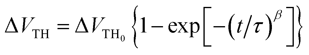 | (2) |
| IGZO thickness | (a) PBTS 60 °C | (b) PBTS 80 °C | ||
|---|---|---|---|---|
| β | τ | β | τ | |
| 10 nm | 0.36 | 5.99 × 10⁶ | 0.46 | 2.57 × 10⁴ |
| 6 nm | 0.33 | 3.06 × 10⁷ | 0.44 | 9.59 × 10⁴ |
Conclusion
We fabricated and characterized IGZO TFTs with ultra-thin channels, and IGZO active layers were successfully prepared by the ALD process. The film thicknesses were varied to 10 and 6 nm by controlling the number of ALD super-cycles to demonstrate the channel thickness dependence. It was found from the analysis of the temperature-dependent electrical conductivity variations that the electronic natures of the ALD-grown IGZO thin films were affected by the film thickness. TFTs using 6 nm-thick IGZO channel exhibited excellent device characteristics such as high μsat of 15.1 cm2 V−1 s−1, steep SS of 0.12 V dec−1, and excellent device uniformity. Small number of trap sites were suggested to be located in the 6 nm-thick IGZO channel from the analysis of the decreasing rate of VGS-dependent thermal activation energy.For the fabricated ALD IGZO TFTs, the ΔVTH values were estimated to be no more than 0.1 V under the PBS and NBS tests for 104 s. Alternatively, the PBTS instabilities were examined as anomalous negative shifts of VTH with lapse in stress time, in which ΔVTH increased from −0.5 to −6.9 V with the increasing temperatures from 40 to 80 °C. The charge-trapping mechanism induced by the holes injected from ITO gate into GI was examined to be one of the main reasons for the time-dependent negative shifts of VTHs because ΔVTHs under PBTS conditions were well fitted by the stretched-exponential equation. Meanwhile, the effects of the ALD process and IGZO composition variations on PBTS instabilities will be investigated in detail in the future. It can be concluded that the device characteristics and the bias temperature stabilities of the IGZO TFTs can be successfully guaranteed by the introduction of the ALD process. Such remarkable device stabilities of TFTs with the IGZO channel prepared by the ALD process can help extend the employment of IGZO TFTs for various applications.
Conflicts of interest
There are no conflicts to declare.Acknowledgements
This work was partly supported by the Korea Evaluation Institute of Industrial Technology through the Korean Government (10079974, Development of core technologies on materials, devices, and processes for TFT backplane and light emitting frontplane with enhanced stretchability above 20%, with application to stretchable display) and by the Kyung Hee University–Samsung Electronics Research and Development Program entitled Flexible Flash Memory Device Technologies for Next-Gen Consumer Electronics.References
- K. Nomura, H. Ohta, A. Takagi, T. Kamiya, M. Hirano and H. Hosono, Nature, 2004, 432, 488 CrossRef PubMed.
- M. J Yu, Y. H Yeh, C. C. Cheng, C. Y. Lin, G. T. Ho, B. C. M. Lai, C. M. Leu, T. H. Hou and Y. J. Chan, IEEE Electron Device Lett., 2012, 33, 47 Search PubMed.
- E. Fortunato, P. Barquinha and R. Martins, Adv. Mater., 2012, 24, 2945 CrossRef PubMed.
- S. Hong, J. W. Park, H. J. Kim, Y. Kim and H. J. Kim, J. Inf. Disp., 2016, 17, 65 CrossRef.
- Y. Li, R. Yao, H. Wang, X. Wu, J. Wu, X. Wu and W. Qin, ACS Appl. Mater. Interfaces, 2017, 9, 1031 Search PubMed.
- J. Sheng, H. J. Lee, S. Oh and J. S. Park, ACS Appl. Mater. Interfaces, 2016, 8, 33821 CrossRef PubMed.
- S. M. Yoon, N. J. Seong, K. J. Choi, G. H. Seo and W. C. Shin, ACS Appl. Mater. Interfaces, 2017, 9, 22676 CrossRef PubMed.
- V. Miikkulainen, M. Leskela, M. Ritala and R. L. Puurunen, J. Appl. Phys., 2013, 113, 021301 CrossRef.
- J. T. Tanskanen, C. Hägglaund and S. F. Bent, Chem. Mater., 2014, 26, 2795 CrossRef.
- J. Lu, J. W. Elam and P. C. Stair, Surf. Sci. Rep., 2016, 71, 410 CrossRef.
- Y. H. Wang, Q. Ma, L. L. Zheng, W. J. Liu, S. J. Ding, H. L. Lu and D. W. Zhang, IEEE Trans. Electron Devices, 2016, 63, 1893 Search PubMed.
- S. H. Bang, S. J. Lee, J. H. Park, S. Y. Park, W. H. Jeong and H. T. Jeon, J. Appl. Phys., 2009, 42, 235102 Search PubMed.
- S. W. Chae, et al., Trans. Electr. Electron. Mater., 2017, 18, 155 Search PubMed.
- Q. Ma, et al., Nanoscale Res. Lett., 2018, 13, 4 CrossRef PubMed.
- J. Y. Heo, S. B. Kim and R. G. Gordon, Appl. Phys. Lett., 2012, 101, 113507 CrossRef.
- K. A. Kim, M. J. Park, W. H. Lee and S. M. Yoon, J. Appl. Phys., 2015, 118, 234504 CrossRef.
- J. T. Jang, J. Park, B. D. Ahn, D. M. Kim, S. J. Choi, H. S. Kim and D. H. Kim, Appl. Phys. Lett., 2015, 106, 123505 CrossRef.
- Y. Y. Nam, H. O. Kim, S. H. Cho and S. H. K. Park, RSC Adv., 2018, 8, 5622 RSC.
- M. K. Ryu, S. H. K. Park, C. S. Hwang and S. M. Yoon, Solid-State Electron., 2013, 89, 171 CrossRef.
- K. Nomura, T. Kamiya, H. Ohta, M. Hirano and H. Hosono, Appl. Phys. Lett., 2008, 93, 192107 CrossRef.
- K. H. Ji, et al., Appl. Phys. Lett., 2011, 98, 103509 CrossRef.
- K. Takechi, M. Nakata, T. Eguchi, H. Yamaguchi and S. Kaneko, J. Appl. Phys., 2009, 48, 010203 CrossRef.
- J. W. Jeong, J. K. Jeong, J. S. Park, Y. G. Mo and Y. T. Hong, J. Appl. Phys., 2010, 49, 03CB02 Search PubMed.
- C. X. Huang, J. Li, X. W. Ding, J. H. Zhang, X. Y. Jiang and Z. L. Zhang, Superlattices Microstruct., 2015, 83, 367 CrossRef.
- J. S. Park, J. K. Jeong, Y. G. Mo, H. D. Kim and C. J. Kim, Appl. Phys. Lett., 2008, 93, 033513 CrossRef.
- H. R. Im, H. S. Song, J. W. Jeong, Y. W. Hong and Y. T. Hong, J. Appl. Phys., 2015, 54, 03CB03 CrossRef.
- H. S. Shin, Y. S. Rim, Y. G. Mo, C. G. Choi and H. J. Kim, Phys. Status Solidi A, 2011, 9, 2231 CrossRef.
- J. H. Song, N. R. Oh, B. D. Anh, H. D. Kim and J. K. Jeong, IEEE Electron Device Lett., 2016, 63, 1054 Search PubMed.
- J. M. Lee, I. T. Cho, J. H. Lee and H. I. Kwon, Appl. Phys. Lett., 2008, 93, 093504 CrossRef.
- X. Du, B. T. Flynn, J. R. Motley, W. F. Stickle, H. Bluhm and G. S. Herman, ECS J. Solid State Sci. Technol., 2014, 3, Q3045 CrossRef.
| This journal is © The Royal Society of Chemistry 2018 |