DOI:
10.1039/C8RA03566K
(Paper)
RSC Adv., 2018,
8, 22887-22896
Novel double anisotropic conductive flexible composite film endued with improved luminescence
Received
25th April 2018
, Accepted 15th June 2018
First published on 21st June 2018
Abstract
Brand-new double anisotropic conductive flexible composite films (ACFs) were firstly put forward, devised and fabricated. The flexible array composite films were constructed via electrospinning using highly aligned Janus nanoribbons as conductive and constitutive units. The Janus nanoribbon consists of two parts, which are respectively conducting side and insulating-luminescent side. The Janus nanoribbons array composite film has two layers, and the two layers are combined tightly to form a top-to-bottom structure. In the composite film, the length direction of the Janus nanoribbons (namely conducting direction) in the two layers is perpendicular, so that a composite film with double electrically conductive anisotropy is achieved. In addition, by adjusting the content of PANI, conductive anisotropy of each layer of the composite film can be tuned, and the conductance in the conducting direction is about 108 times stronger than that in the insulating direction. The Janus nanoribbon array composite films also have tunable and improved luminescent properties, achieving bi-functionality of double anisotropically electrical conduction and luminescence. The proposed design concept and preparation technology will provide theoretical and technical support for the design and fabrication of novel multifunctional ACFs.
Introduction
Recently, study on anisotropic conductive films (denoted ACFs for short) has become one of the hottest topics in the realm of materials science and ACFs have been widely applied in the field of high-technology1,2 due to their various advantages.3,4 To date, several types of ACF have been prepared. Type I ACFs are conducting along the thickness direction of the membrane and insulated along the membrane surface.5 This type of ACF has applications in smart card6 and electronic fields.7 On the basis of type I ACFs, type II ACFs are further developed and have different conductance along the two perpendicular directions of their surfaces.8 The type II ACFs are considered to be ideal carriers for electronic components and simultaneously realize parallel transmission of electrical current, which is unattainable by other interconnected materials for electronic components. Basically, there are three methods to fabricate the type II ACFs. In the first method, the conductive material is directionally arranged in the polymer matrix so that the material has anisotropic conductive properties.9 In the second method, the conductive fillers are sequentially assembled into ordered one-dimensional chains or strip assemblies in the polymeric matrix.10 For the third method, micro- or nanoribbons are used to design and prepare anisotropic conductive materials. For example, tri-color flag-liked microribbons array films11 and Janus nanoribbons array films12,13 have been fabricated, which achieved large differences in the conductance along the length and the vertical directions of the films, and succeeded in obtaining anisotropic films with high-conductivity. With the development of nanoscience and nanotechnology, in the future, varieties of ACFs are undoubtedly needed to manufacture advanced electronic nanodevice, and therefore, it is an imperative and meaningful subject of study to construct brand-new ACFs.
Polyaniline (PANI) has become one of the most studied conductive polymers for its following unique advantages: (a) simple synthesis;14 (b) chemical stability15 and excellent electrochemical performance;16 (c) unique doping phenomenon;17 (d) high conductivity;18 (e) good environmental stability.19 As the above merits mentioned, PANI has been used in electromagnetic shielding technology,20 anti-static technology,21 solar cells,22–24 catalytic materials and secondary battery materials.25 Rare earth (RE) complexes, especially terbium complexes, have unique fluorescent performances due to the f–f electron transition of RE3+ ions, which have been widely used as phosphors,26 magneto-optic storage materials,27 electronic information storage materials28 and etc.29
Electrospinning technology is considered to be one of the simplest methods for preparing micro- and nanomaterials by processing a viscous solution under high voltage into continuous fibers of micron to nanometer diameter.30,31 The technique has been extensively applied in the fields of photoelectric devices,32,33 electronic equipments,34–36 oil-water separation and photocatalysis, etc.37–39 Compared with other methods for preparing type II ACFs, electrospinning technology has some crucial advantages such as simple process, low power consumption and large area of the fabricated films. Especially, some special nanostructures, such as Janus nanoribbon, can only be prepared by electrospinning for now.
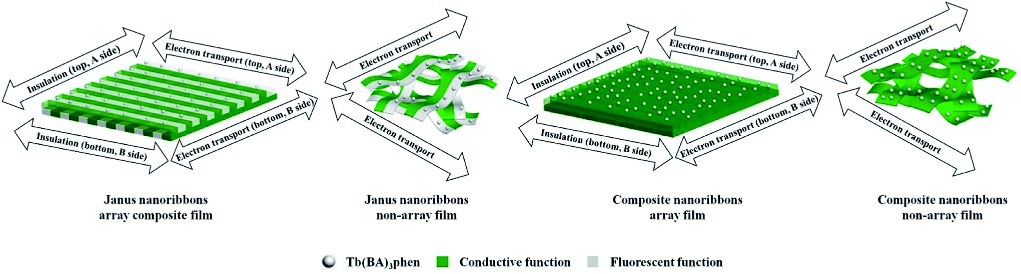
In this work, we creatively propose and construct the composite film consisting of two-layer vertical flexible Janus nanoribbon array films. This newly conceived and designed composite film is composed of vertical two layers which are discerned from the length orientations of Janus nanoribbons in the double-layer arrays (called A side and B side), forming a top-to-bottom structure. Here, Janus nanoribbon, as the constituent and conductive unit of the composite film, consists of PANI/polymethylmethacrylate (PMMA) as conducting side and Tb(BA)3phen/PMMA as insulating-luminescent side. A side is conducting along the horizontal orientation, and the vertical orientation is insulated, whereas the B side is exactly the opposite. Because the Janus nanoribbons on A side and B side have different conducting directions, the electrical property of this film is defined as “double electrically conductive anisotropy”. To demonstrate the benefits of Janus nanoribbon array composite film, three counterpart contrast samples are also prepared. Finally, a series of modern determination techniques are used to characterize the final samples, and some new results are successfully acquired.
Experimental sections
Chemicals
Benzoylperoxide (BPO), methylmethacrylate (MMA), Tb4O7, benzoic acid (BA), concentrated nitric acid, aniline (ANI), 1,10-phenanthroline (phen), ammonium persulfate (APS), (1S)-(+)-camphor-10 sulfonic acid (CSA), N,N-dimethylformamide (DMF), CHCl3, and anhydrous ethanol were used. The purity of Tb4O7 was 99.99%. All the reagents used in the experiments were analytically pure and bought from Aladdin Chemistry Co., Ltd.
Preparation of terbium complexes. Tb(BA)3phen complexes were prepared on the basis of the paper.40
Fabrication of PMMA. PMMA was fabricated on the basis of the ref. 41.
Preparation of spinning solutions. Janus nanoribbons were constructed by two different spinning solutions. Spinning solution I was composed of Tb(BA)3phen, PMMA, CHCl3 and DMF, which was used for fabricating the insulating-luminescent side. These materials were directly mixed and magnetically stirred for 48 h, and their amounts were listed in Table 1. With regard to preparing spinning solution II to fabricate the conducting side, 1.0000 g of PMMA was dissolved in the mixture of CSA, 6.0000 g of CHCl3 and 0.8000 g of DMF, and then different quantities of ANI were introduced into the above mixture under magnetic agitation at room temperature for 24 h (called solution A). Oxidant APS was dissolved in the mixture of 1.2000 g of DMF and 6.0000 g of CHCl3 for 2 h under magnetic stirring (denoted as solution B). The two solutions were placed into a refrigerator at 0 °C for one hour. Then, solution B was dropwise added in solution A in an ice-bath and magnetically stirred for 3 h. At last the mixture was placed into the refrigerator for one day. The compositions and dosages to prepare spinning solution II were summarized in Table 2. The Janus nanoribbons array composite films prepared by Sa3//Sb1, Sa3//Sb2, Sa3//Sb3, Sa3//Sb4 and Sa3//Sb5 were respectively denoted as S1–S5.
Table 1 Compositions and quantities of the spinning solution I
| Spinning solution I |
Tb(BA)3phen [g] |
DMF [g] |
CHCl3 [g] |
PMMA [g] |
| Sa1 |
0.0500 |
2.0000 |
12.0000 |
1.0000 |
| Sa2 |
0.1000 |
2.0000 |
12.0000 |
1.0000 |
| Sa3 |
0.1500 |
2.0000 |
12.0000 |
1.0000 |
| Sa4 |
0.2000 |
2.0000 |
12.0000 |
1.0000 |
| Sa5 |
0.2500 |
2.0000 |
12.0000 |
1.0000 |
Table 2 Compositions and quantities of the spinning solution II
| Spinning solution II |
PANI:PMMA [wt%] |
ANI [g] |
CSA [g] |
APS [g] |
PMMA [g] |
| Sb1 |
30% |
0.3000 |
0.5168 |
0.7352 |
1.0000 |
| Sb2 |
40% |
0.4000 |
0.7490 |
0.9780 |
1.0000 |
| Sb3 |
50% |
0.5000 |
0.9364 |
1.2324 |
1.0000 |
| Sb4 |
60% |
0.6000 |
1.1236 |
1.4700 |
1.0000 |
| Sb5 |
70% |
0.7000 |
1.3108 |
1.7156 |
1.0000 |
Fabrication of double electrically conductive anisotropy flexible composite film made of Janus nanoribbons array
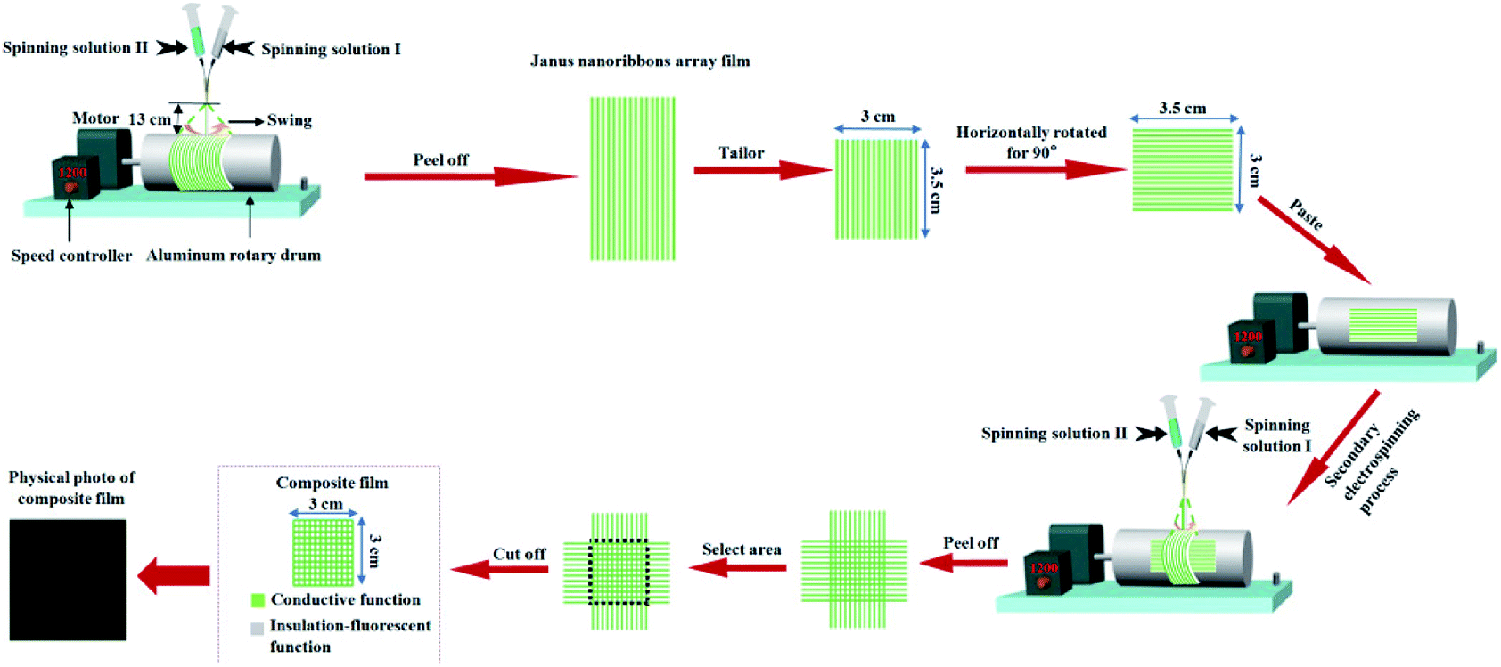
The schematic of the experimental procedure for electrospinning is presented in Fig. 1. Spinning solution I and II were respectively loaded into two plastic syringes which were bundled together. An aluminum rotary drum was placed approximately 13 cm away from the point of the self-made parallel spinneret and used as a collector. The rotational speed of the aluminium rotary drum was 1200 r/min. The voltage of the positive direct current (DC) was 6 kV. The temperature and atmospheric relative humidity respectively were 15–20 °C and 10–15%. Under these spinning conditions, electrospinning process was carried out to produce stable, continuous Janus nanoribbons array. To achieve double electrically conductive anisotropy flexible composite films, three main steps were adopted. Firstly, single electrically conductive anisotropy film (named as A side) was fabricated through using both 3 mL of spinning solution I and II, and then peeled off from the collector. The as-obtained film was tailored into 3 cm in the vertical orientation and 3.5 cm along with the horizontal orientation of the Janus nanoribbons. Secondly, the single electrically conductive anisotropy film composed of Janus nanoribbons array (A side) was rotated to 90°, and then pasted it onto the aluminum rotary drum. Thirdly, the second electrospinning was performed to fabricate another-layer electrically conductive anisotropy film (denoted as B side), and the used amounts of spinning solution I and solution II were the same as those for the first electrospinning process, which were also 3 mL respectively. After both solutions were consumed simultaneously, the experiment was stopped and the final sample was removed from the collector, and then the freshly prepared composite film was cut into 3 × 3 cm2. At this point, double anisotropic electrically conductive flexible composite film (composed of A side and B side) with the area of 3 × 3 cm2 was successfully prepared.
 |
| | Fig. 1 Schematic diagram for the fabrication of double electrically conductive anisotropy flexible composite films. | |
To highlight the merits of double electrically conductive anisotropy composite film, Janus nanoribbons non-array film (Sa3//Sb1), composite nanoribbons array film (made from Sa3/Sb1) and composite nanoribbons non-array film (Sa3/Sb1), as contrast samples, were also fabricated. The preparation method of composite nanoribbons is shown as below: spinning solution I (Sa3) and II (Sb1) were mingled with the volume ratio of 1![[thin space (1/6-em)]](https://www.rsc.org/images/entities/char_2009.gif) :1 and then fabricated by the electrospinning technique with a single spinneret. Also, array films were prepared by using aluminum rotary drum as collector, while non-array films were fabricated by using iron wire-net as collector. The spinning conditions for preparing the three contrast samples were the same as those for fabricating double electrically conductive anisotropy composite film. Janus nanoribbons non-array film (PANI: PMMA = 30%) was named as S6 (Sa3//Sb1). The composite nanoribbons array film was denoted as S7 (Sa3/Sb1) and composite nanoribbons non-array film was defined as S8 (Sa3/Sb1).
:1 and then fabricated by the electrospinning technique with a single spinneret. Also, array films were prepared by using aluminum rotary drum as collector, while non-array films were fabricated by using iron wire-net as collector. The spinning conditions for preparing the three contrast samples were the same as those for fabricating double electrically conductive anisotropy composite film. Janus nanoribbons non-array film (PANI: PMMA = 30%) was named as S6 (Sa3//Sb1). The composite nanoribbons array film was denoted as S7 (Sa3/Sb1) and composite nanoribbons non-array film was defined as S8 (Sa3/Sb1).
Characterizations
The equipments of field emission scanning electron microscopy (FESEM, XL-30), energy dispersive spectroscopy (EDS) connected to FESEM and optical microscope (OM) were respectively used to test the morphology and size, element contents, and internal structure of the samples. A fluorescence spectrophotometer F-7000 was employed to investigate the luminescent properties of final composite films. Electrical properties of the samples were measured via the ECOPIA HMS-3000 Hall effect measurement system.
Results and discussion
Morphology and internal structure
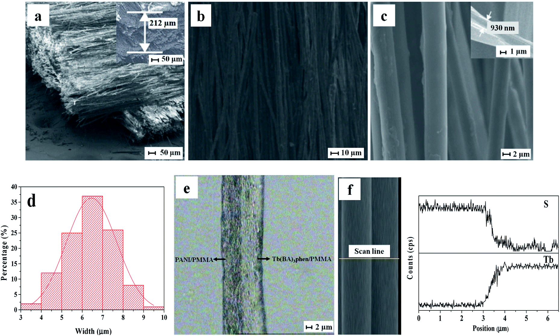
SEM image of cross-section of the Janus nanoribbons array composite film, SEM images, EDS spectrum, OM image and the histogram of width distribution of the Janus nanoribbons in the composite film are demonstrated in Fig. 2. It is clearly observed from Fig. 2a that the Janus nanoribbons are perpendicular in the two layers of the Janus nanoribbons array composite film, and the thickness of the monolayer film is about 212 μm. Such framework insures that the conducting orientations of the two layers (i.e. the length direction of Janus nanoribbons) are perpendicular to each other. Furthermore, in each layer of this typed film, most of the Janus nanoribbons are well-arranged in the unified orientation to insure electrically conductive anisotropy, as seen in Fig. 2b. Fig. 2c displays the SEM image of the Janus nanoribbons array composite film at high magnification. Obviously, all of the wide-sides of the nanoribbons are pointing up, with very few exceptions. The possible reason is that this arrangement helps the nanoribbons have a state of more stable and low-potential energy when they are collected on the collector. The thickness of the Janus nanoribbon is ca. 930 nm, as shown in the inset of Fig. 2c; and the width of Janus nanoribbons is ca. 6.64 ± 0.01 μm, as revealed in Fig. 2d. The internal detailed structure of the Janus nanoribbon was further observed through using an optical microscope. A visible asymmetrically bilateral construction can be clearly found for the Janus nanoribbon, as displayed in Fig. 2e. One side of the Janus nanoribbon having the conducting functionality exhibits dark color owing to the existence of PANI, the other side of the Janus nanoribbon possessing insulating-luminescent functionality is transparent. EDS line-scan analyses are also carried out to further demonstrate the Janus structure, where S and Tb elements respectively stand for CSA doped in PANI and Tb(BA)3phen, as depicted in Fig. 2f. It can be seen that S and Tb respectively distribute in the different regions of the Janus nanoribbon, which is consistent with the bilateral structure of Janus nanoribbon. Based on the above-mentioned analytical results, we can reasonably reach the conclusion that the Janus nanoribbons array composite films composed of well-aligned Janus nanoribbons have been successfully manufactured.
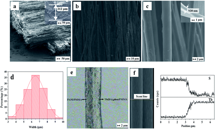 |
| | Fig. 2 SEM image of cross-section of the Janus nanoribbons array composite film (a); SEM images at low (b) and high (c) magnifications, histogram of width distribution (d) of Janus nanoribbons in the composite film; OM image (e) and EDS line-scan analysis (f) of a single stripe of Janus nanoribbon. | |
SEM images of Janus nanoribbons non-array film, the composite nanoribbons array film and non-array film, and histogram of width distribution of composite nanoribbons in composite nanoribbons array film are illustrated in Fig. 3. SEM micrograph of the Janus nanoribbons non-array film is illustrated in Fig. 3a, and it can be clearly seen that the arrangement of the nanoribbons was randomly disordered. As seen from Fig. 3b, the nanoribbons in the composite nanoribbons array film are well arranged in the same orientation, and the width of composite nanoribbons is ca. 6.59 ± 0.09 μm (Fig. 3c). It is distinctly seen from Fig. 3d that the arrangement of the composite nanoribbons in the composite nanoribbons non-array film is out of order.
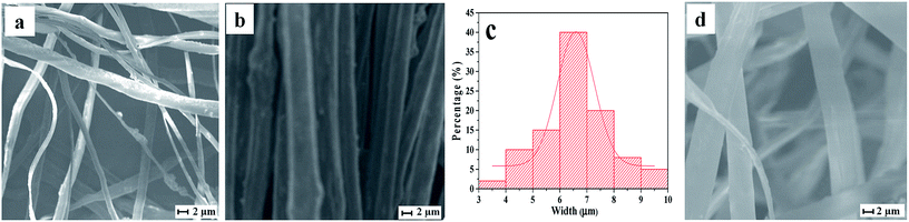 |
| | Fig. 3 SEM images of Janus nanoribbons non-array film (a) and the composite nanoribbons array film (b); histogram of width distribution (c) of the composite nanoribbons in composite nanoribbons array film; SEM image of composite nanoribbons non-array film (d). | |
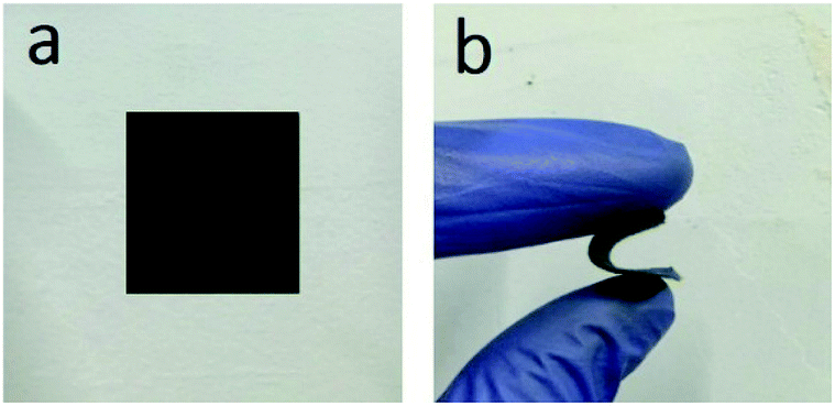
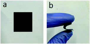
Fig. 4 displays the digital photos of final Janus nanoribbons array composite film. It is apparent that the film can be folded freely, demonstrating the good flexible performance which is a significant factor for the application in flexible electronic devices.
 |
| | Fig. 4 Digital photos of double electrically conductive anisotropy flexible composite film at unbent (a) and bent status (b). | |
Luminescent performance
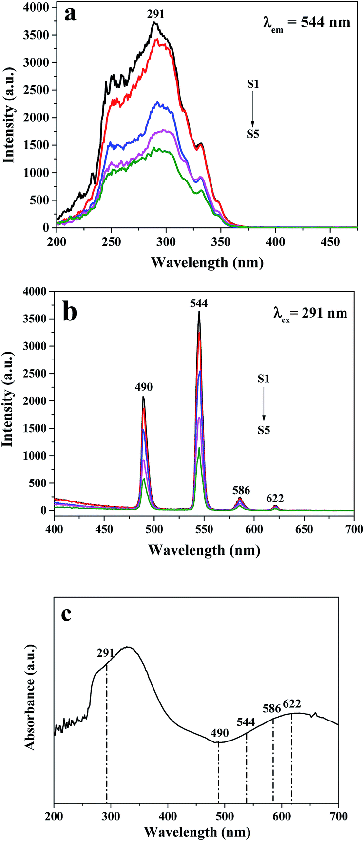
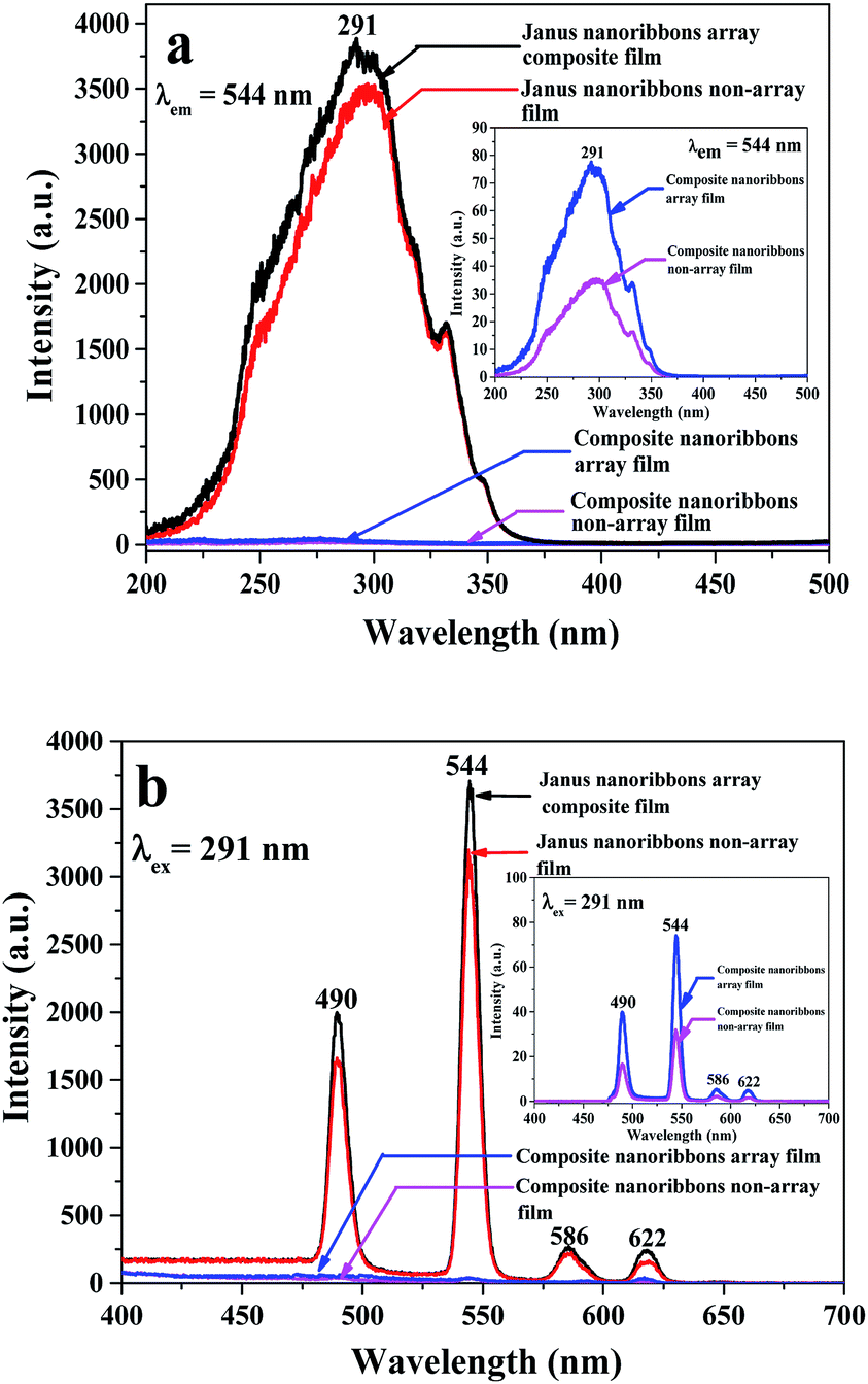
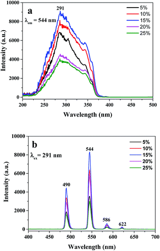
A series of Tb(BA)3phen/PMMA nanoribbons with different amounts of Tb(BA)3phen complexes were prepared to seek out the optimum content of Tb(BA)3phen complexes to PMMA of the Janus nanoribbons in the composite film. The Tb(BA)3phen/PMMA nanoribbons were respectively prepared via using spinning solutions Sa1 to Sa5 by traditional electrospinning method with single nozzle. The excitation and emission spectra of Tb(BA)3phen/PMMA nanoribbons are indicated in Fig. 5. As shown in excitation spectra (Fig. 5a), a wide excitation band ranging from 200 to 375 nm with a strongest peak at 291 nm can be observed, which is attributed to π → π* electron transition of ligands under the condition that the monitoring wavelength is set to 544 nm. At the same time, characteristic emission peaks (Fig. 5b) of Tb3+ are found under 291 nm UV light excitation, which are respectively located at 490, 544, 586 and 622 nm. These peaks are respectively ascribed to 5D4 → 7F6, 5D4 → 7F5, 5D4 → 7F4 and 5D4 → 7F3 energy level transitions of Tb3+, and the green light emission at 544 nm assigned to 5D4 → 7F5 hypersensitive transition is dominant. Also as seen from Fig. 5, the luminescent intensity of the Tb(BA)3phen/PMMA nanoribbons is gradually increased and then weakened with adding more Tb(BA)3phen complexes. When the concentration of Tb(BA)3phen complexes to PMMA is 15%, the strongest luminescent intensity is obtained, implying that the optimum percentage of Tb(BA)3phen complexes is 15% in Tb(BA)3phen/PMMA nanoribbons. Thus, the content of 15% for Tb(BA)3phen is applied to prepare Janus nanoribbons in this work.
 |
| | Fig. 5 Excitation (a) and emission (b) spectra of Tb(BA)3phen/PMMA nanoribbons containing various contents of Tb(BA)3phen. | |
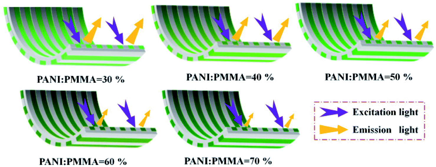
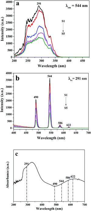
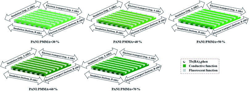
In order to more deeply discuss the luminescent performance of Janus nanoribbons array composite film, the weight ratios of PANI to PMMA are tuned from 30% to 70% when the content of Tb(BA)3phen complexes to PMMA is fixed at 15%, as indicated in Fig. 6, in which the excitation and emission spectra of A side of Janus nanoribbons array composite film are shown, and the excitation and emission spectra of B side are almost the same as those of A side. It is not difficult to see that the excitation and emission intensities of these films decrease with adding more amount of PANI. To explain the influence of various contents of PANI on the luminescence, schematic illustrations of the excitation and emission light in Janus nanoribbons array composite film with different percentages of PANI are illustrated in Fig. 7. Fig. 6c shows the UV-Vis absorption curve of PANI, in which it can be clearly found that PANI can strongly absorb the UV light and also absorb the light in the wavelength ranging from 400 to 760 nm. Thus, parts of the excitation light (291 nm) and emission light (490, 544, 586 and 622 nm) in the Janus nanoribbons array composite film are absorbed by dark-colored PANI, resulting in the weakened intensities of excitation and emission light. Furthermore, the absorption of light becomes stronger and the colors of the samples become darker with addition of more PANI into Janus nanoribbons array composite film.
 |
| | Fig. 6 Excitation (a) and emission (b) spectra of Janus nanoribbons array composite films containing various contents of PANI to PMMA, and UV-Vis absorbance spectrum of PANI (c). | |
 |
| | Fig. 7 Schematic illustrations of the excitation and emission light in Janus nanoribbons array composite film with different percentages of PANII. | |
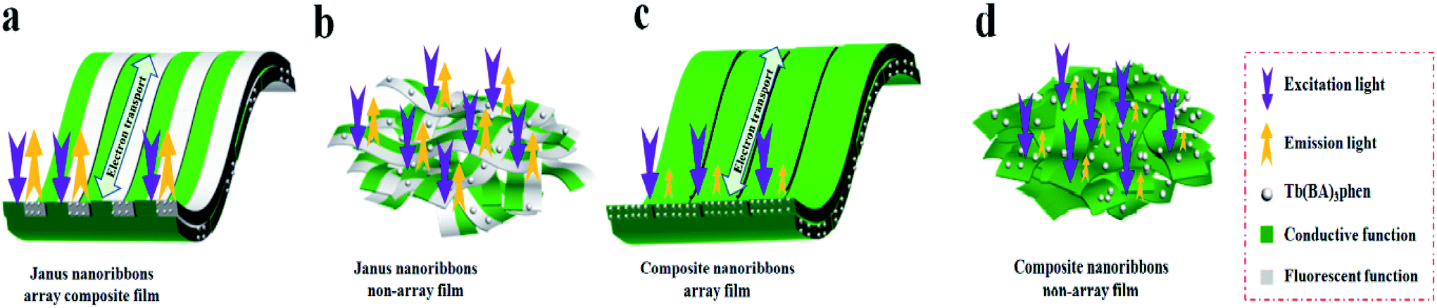
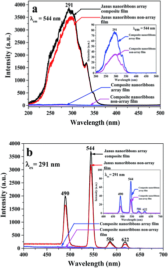
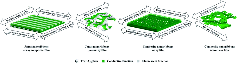
To highlight the excellent luminescent performance of the Janus nanoribbons array composite film, the luminescent properties of Janus nanoribbons non-array film, composite nanoribbons array film and composite nanoribbons non-array film are also measured, and the results are illustrated in Fig. 8. Fig. 8a and b show that the Janus nanoribbons array composite film and Janus nanoribbons non-array film have visibly stronger luminescent intensity than the counterpart composite nanoribbons array film and composite nanoribbons non-array film. Fig. 9 is the schematic diagrams that shows comparisons of the luminescent characteristics of the above four samples. Both of the Janus nanoribbons array composite film and Janus nanoribbons non-array film constructed by the unit of Janus nanoribbon realize efficient separation of PANI from Tb(BA)3phen. Hence, the absorptions of excitation and emission light by PANI are strongly weakened. The composite nanoribbons array film and composite nanoribbons non-array film are both constructed by the unit of the composite nanoribbon, in which the Tb(BA)3phen and PANI are uniformly distributed, leading to the result that bottle-green PANI greatly absorbs and decreases the excitation and emission light. Because the Janus nanoribbons array composite film (Fig. 9a) is comprised of highly ordered Janus nanoribbons, the composite film surface is imporous. It is difficult for the excitation light to approach the Janus nanoribbons in the underlying layers by passing through the topmost layers, so emission light is mainly generated from the Janus nanoribbons in the topmost layers without decrease. For Janus nanoribbons non-array film (Fig. 9b), the Janus nanoribbons are disorganized and the surface of the film is incompact. In this situation, a portion of excitation light will pass the gaps of the incompact topmost layers to approach the Janus nanoribbons in the underlying layers and it is absorbed by the Janus nanoribbons in the topmost layers. Likewise, the emission light must pass the gaps in the topmost layers and is also absorbed. As a consequence, the Janus nanoribbons array composite film (Fig. 8) exhibits slightly higher luminescent intensity than Janus nanoribbons non-array film. Just as the before-mentioned reason, composite nanoribbons array film (Fig. 9c) has higher luminescent intensity than composite nanoribbons non-array film (Fig. 9d), as revealed in the insets of Fig. 8. Judging from the before-mentioned analyses of the luminescent properties, we can justifiably draw one conclusion that the Janus nanoribbons array composite films have superior properties than the three contrast samples.
 |
| | Fig. 8 Excitation (a) and emission (b) spectra of Janus nanoribbons array composite film and the three contrast samples; insets are the enlarged spectra of the composite nanoribbons array film and non-array film. | |
 |
| | Fig. 9 Schematic diagrams of excitation and emission light of Janus nanoribbons array composite film and three contrast samples. | |
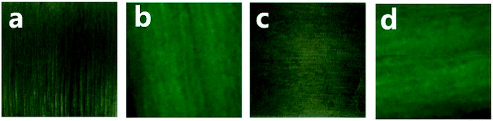
Fig. 10 is physical digital photos of double electrically conductive anisotropy composite film and their emission colors under the 291 nm excitation in darkness. Fig. 10a and c are the physical digital photos of the obverse and reverse sides of the composite film. It is found that the obverse and reverse sides have almost same color owing to the same components and structure, and present excellent filminess. The photos of Fig. 10b and d display the green light emitting from the Janus nanoribbons array composite film under UV illumination of 291 nm.
 |
| | Fig. 10 Physical digital photos of obverse side (a) and reverse side (c) of double electrically conductive anisotropy Janus nanoribbons array composite film and the emission colors of obverse side (b) and reverse side (d) of the composite film under 291 nm excitation in darkness. | |
Fig. 11 is the CIE coordinates chromaticity diagram of Janus nanoribbons array composite film and Janus nanoribbons non-array film under the excitation of 291 nm UV illumination, which shows that the emission color of the Janus nanoribbons array composite film and Janus nanoribbons non-array film is green. As indicated in Fig. 8b, the emission intensity of Janus nanoribbons array composite film (S1) is stronger than that of Janus nanoribbons non-array film (S6), because the PANI in Janus nanoribbons non-array film (S6) absorbs more emission light. It is also seen from Fig. 6c that the PANI can absorb more red light (586, 622 nm) than the green light (544 nm). As a result, the fluorescent color of Janus nanoribbons non-array film is greener.
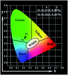 |
| | Fig. 11 CIE chromaticity coordinates diagram of Janus nanoribbons array composite film (S1) and Janus nanoribbons non-array film (S6). | |
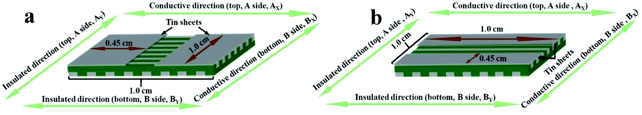
Conductance analysis
The electrical conductivity of the samples was systematically researched. For measuring Janus nanoribbons array composite films, the content of Tb(BA)3phen is fixed at 15% and the contents of PANI to PMMA are ranged from 30%, 40%, 50%, 60%, to 70%. The Janus nanoribbons array composite film consists of top and bottom two layers. The top and bottom layers are respectively denoted as A side and B side. In the two layers, the orientations of parallel (the orientation of conducting) and perpendicular (the orientation of insulating) to the length of the nanoribbons are respectively named as subscript X and Y. The top and bottom layers of the composite film are respectively defined as AX, AY, BX and BY. The measurement methods for the composite film are displayed in Fig. 12. The areas of the products are cut to 1 × 1 cm2, and a couple of tin sheets with the areas of 1 × 0.45 cm2 are used as electrodes which are pasted onto the surface of the products via using the conductive resin. The two tin sheets are placed in opposite positions with a distance of 0.1 cm. The electrically conductive performances of the double electrically conductive anisotropy flexible Janus nanoribbons array composite films containing different amounts of PANI and all the contrast samples are summarized in Table 3. As obviously observed from Table 3, for the Janus nanoribbons array composite films, with introducing more PANI, the conductance along with AX and BX improves dramatically, while in contrast, the changes of the conductance along with AY and BY are relatively insignificant. Hence, the conductance of conducting directions of the samples can be adjusted by changing the contents of PANI, leading to the adjustable anisotropic conduction degree. Moreover, the maximum value of X/Y can reach up to ca. 108 times (the highest value available at present) while the contents of PANI to PMMA is 60–70%. Fig. 13 exhibits the schematics of conductive mechanism of Janus nanoribbons array composite films. Once the current is generated, electrons can move unimpededly along with the length orientation of Janus nanoribbons in the composite film. As the content of PANI increases, the increase in conductance is ascribed to the generation of more continuous network of PANI which makes the charge transport more high-efficiency. In comparison, for the insulating orientations, benefit from the abundance of insulating sides of Janus nanoribbons which hinder the charge transfer, the conductance value is always in the order of 10−12 S with the changes of PANI contents. Compared with all the contrast samples, the conductance of conducting direction of the Janus nanoribbons array composite film is the strongest under the same contents and components, as also seen in Table 3. The Janus nanoribbons array composite film has strong anisotropy (S1:X/Y ≈ 104). The conductance ratios of X/Y of the Janus nanoribbons non-array film and the composite nanoribbons non-array film (X and Y are two perpendicular directions) are respectively ca. 1, meaning that no anisotropy is obtained. The composite nanoribbons array film possesses weak anisotropy (X/Y ≈ 8, X: conducting direction, Y: insulating direction). The schematics of conductive mechanism for Janus nanoribbons array composite film and the three contrast samples are depicted in Fig. 14. The Janus nanoribbons in the Janus nanoribbons array composite film are ordered in the same orientation, so the direction of current flow is uniform. By comparison, the flow orientation of the current is chaotic due to the fact that the Janus nanoribbons in the Janus nanoribbons non-array film are chaotic. In such situation, the electrical conduction exhibits in every orientation of the non-array film, resulting in the consequence that the conductance in one particular orientation is reduced. The composite nanoribbons array film and the composite nanoribbons non-array film have clearly lower conductance than Janus nanoribbons array composite film because the insulating-luminescent materials are equably decentralized in the composite nanoribbons, and this phenomenon blocks the generation of continuous conductive network to some extent. The orientation of current flows in Janus nanoribbons array composite film is settled, that is, the horizontal orientation to the length of the nanoribbons is conducting and the vertical orientation is insulating, and thus the conductance ratio of the film is relatively stronger. The weak anisotropy degree of the composite nanoribbons array film is because composite nanoribbons are fitly aligned in the film, the interfaces among the composite nanoribbons can serve as the insulating materials, however, the insulating property of these interfaces is not sufficiently strong. The composite non-array film exhibits electrical conduction in all directions, so that no electrically conductive anisotropy phenomenon in film is found, and the conductance ratio of X/Y is ca. 1. As clearly seen from Table 3, the value of AX/Y/BX/Y for the Janus nanoribbons array composite film is ca. 1, which indicates that A side and B side have little difference in electrically conductive anisotropy, implying that A side and B side of the composite film have identical structures and components. All the before-mentioned analyses illustrate that the Janus nanoribbons array composite film has successfully achieved the double electrically conductive anisotropy.
 |
| | Fig. 12 Schematic illustrations of conductance test for double electrically conductive anisotropy flexible Janus nanoribbons array composite film: conducting orientation (a) and perpendicular orientation (b). | |
Table 3 Conductances of Janus nanoribbons array composite films containing various amounts of PANI and the contrast samples
| Samples |
Conductance (S) |
Anisotropy degree |
AX/Y/BX/Y |
| AX |
AY |
BX |
BY |
AX/Y |
BX/Y |
| Janus nanoribbons array composite film |
| (S1, PANI:PMMA = 30%) |
1.62 × 10⁻⁸ |
1.28 × 10⁻¹² |
1.64 × 10⁻⁸ |
1.27 × 10⁻¹² |
1.24 × 10⁴ |
1.29 × 10⁴ |
Medium |
0.96 |
| (S2, PANI:PMMA = 40%) |
6.61 × 10⁻⁸ |
1.79 × 10⁻¹² |
6.41 × 10⁻⁸ |
1.75 × 10⁻¹² |
3.67 × 10⁴ |
3.67 × 10⁴ |
Medium |
1.00 |
| (S3, PANI:PMMA = 50%) |
1.73 × 10⁻⁶ |
2.99 × 10⁻¹² |
1.75 × 10⁻⁶ |
2.88 × 10⁻¹² |
5.80 × 10⁵ |
6.08 × 10⁵ |
Strong |
0.95 |
| (S4, PANI:PMMA = 60%) |
2.32 × 10⁻⁴ |
1.79 × 10⁻¹² |
2.34 × 10⁻⁴ |
1.76 × 10⁻¹² |
1.29 × 10⁸ |
1.32 × 10⁸ |
Very strong |
0.98 |
| (S5, PANI:PMMA = 70%) |
5.32 × 10⁻⁴ |
1.22 × 10⁻¹² |
5.25 × 10⁻⁴ |
1.22 × 10⁻¹² |
4.35 × 10⁸ |
4.30 × 10⁸ |
Very strong |
1.01 |
|
| Janus nanoribbons non-array composite film |
| (S6, PANI:PMMA = 30%) |
1.05 × 10⁻⁸ |
1.03 × 10⁻⁸ |
1.03 × 10⁻⁸ |
1.02 × 10⁻⁸ |
1.01 |
1.00 |
None |
1.01 |
|
| Composite nanoribbons array film |
| (S7, PANI:PMMA = 30%) |
1.65 × 10⁻⁹ |
2.03 × 10⁻¹⁰ |
1.68 × 10⁻⁹ |
2.01 × 10⁻¹⁰ |
8.12 |
8.36 |
Weak |
0.97 |
|
| Composite nanoribbons non-array film |
| (S8, PANI:PMMA = 30%) |
1.02 × 10⁻⁹ |
1.29 × 10⁻⁹ |
1.08 × 10⁻⁹ |
1.27 × 10⁻⁹ |
0.79 |
0.85 |
None |
0.93 |
 |
| | Fig. 13 Schematic diagrams of conductive mechanism and color gradient doped with various contents of PANI for Janus nanoribbons array composite film. | |
 |
| | Fig. 14 Conductive schematic diagrams of Janus nanoribbons array composite film and the contrast samples. | |
Conclusions
To sum up, brand-new double electrically conductive anisotropy flexible Janus nanoribbons array composite films have been firstly manufactured by using electrospinning method. The flexible composite film consists of highly aligned Janus nanoribbons which are composed of conducting side and insulating-luminescent side. The composite film has a top-to-bottom structure, and the directions of length (i.e. the conducting directions) of the Janus nanoribbons in the top and bottom layers are perpendicular, making the composite film possess double electrically conductive anisotropy. The degree of electrically conductive anisotropy in each layer of the flexible Janus nanoribbons array composite films can be adjustable by changing the percentages of PANI, and the conductance in the conducting orientation reaches up to about 108 times stronger than that in the insulating orientation. The Janus nanoribbons array composite films are simultaneously endowed with luminescent performance to achieve bi-functionality. This new composite film has possible applications in the fields of molecular electronics, nanodevices, etc. More importantly, this design idea and manufacture technology will provide supports for devising and constructing new-typed particular nanomaterials with multi-functionality.
Conflicts of interest
There are no conflicts of interest to declare.
Acknowledgements
This work was financially supported by National Natural Science Foundation of China (51573023, 50972020), Natural Science Foundation of Jilin Province (20170101101JC, 20180520011JH), Industrial Technology Research and Development Project of Jilin Province Development and Reform Commission (2017C052-4), Science and Technology Research Planning Project of the Education Department of Jilin Province during the 13th Five-Year Plan Period (JJKH20170608KJ), Innovative Foundation (XJJLG-2017-04) and Youth Foundation (XQNJJ-2016-01, XQNJJ-2017-17) of Changchun University of Science and Technology.
Notes and references
- X. Zhou, M. Torabi, J. Lu, R. Q. Shen and K. L. Zhang, ACS Appl. Mater. Interfaces, 2014, 6, 3058–3074 CrossRef PubMed.
- Y. Liu, J. Y. Zhou, W. B. Fu, P. Zhang, X. J. Pan and E. Q. Xie, Carbon, 2017, 114, 187–197 CrossRef.
- H. Y. Guo, C. Y. Lan, Z. F. Zhou, P. H. Sun, D. P. Wei and C. Li, Nanoscale, 2017, 9, 6246–6253 RSC.
- M. Yang, S. J. Sheng, Q. L. Ma, N. Lv, W. S. Yu, J. X. Wang, X. T. Dong and G. X. Liu, Mater. Res., 2016, 19, 308–313 CrossRef.
- X. Wang, S. A. Chaudhry, W. S. Hou and X. F. Jia, Int. J. Mol. Sci., 2017, 18, 335 CrossRef PubMed.
- S. M. S. Privitera, G. Litrico, M. Camarda, N. Piluso and F. L. Via, Appl. Phys. Express, 2017, 10, 036601 CrossRef.
- E. Drożdż and A. Koleżyński, RSC Adv., 2017, 7, 28898–28908 RSC.
- G. N. Morscher and N. A. Gordon, J. Eur. Ceram. Soc., 2017, 37, 3861–3872 CrossRef.
- M. K. Liu, Y. F. Du, Y. E. Miao, Q. W. Ding, S. X. He, W. W. Tjiu, J. S. Pan and T. X. Liu, Nanoscale, 2015, 7, 1037–1046 RSC.
- Q. L. Ma, W. S. Yu, X. T. Dong, J. X. Wang and G. X. Liu, Nanoscale, 2014, 6, 2945–2952 RSC.
- Q. L. Ma, W. S. Yu, X. T. Dong, M. Yang, J. X. Wang and G. X. Liu, Sci. Rep., 2015, 5, 14583 CrossRef PubMed.
- Q. L. Ma, J. X. Wang, X. T. Dong, W. S. Yu and G. X. Liu, Adv. Funct. Mater., 2015, 25, 2436–2443 CrossRef.
- X. B. Li, Q. L. Ma, J. Tian, X. Xi, D. Li, X. T. Dong, W. S. Yu, X. L. Wang, J. X. Wang and G. X. Liu, Nanoscale, 2017, 9, 18918–18930 RSC.
- H. D. Han, J. M. Kim and Y. L. Kim, Ceram. Int., 2017, 43, 766–770 CrossRef.
- J. N. Ma, W. Liu, B. Quan, X. H. Liang and G. B. Ji, J. Colloid Interface Sci., 2017, 504, 479–484 CrossRef PubMed.
- M. R. Kiran, H. Ulla, M. N. Satyanarayan and G. Umesh, Synth. Met., 2017, 224, 63–71 CrossRef.
- S. Moshtarikhah, N. A. W. Oppers, M. T. D. Groot, J. T. F. Keurentjes, J. C. Schouten and J. V. D. Schaaf, J. Appl. Electrochem., 2017, 47, 51–62 CrossRef.
- A. M. Balakt, C. P. Shaw and Q. Zhang, J. Eur. Ceram. Soc., 2017, 37, 1459–1466 CrossRef.
- P. Q. Wang, J. J. Zhao, L. Y. Wei, Q. F. Zhu, S. H. Xie, J. X. Liu, X. J. Meng and J. Y. Li, Nanoscale, 2017, 9, 3806–3817 RSC.
- H. J. Lee, S. Y. Chung, Y. S. Kim and T. I. Lee, Nano Energy, 2017, 38, 232–238 CrossRef.
- J. S. Kang, M. Ke and Y. J. Hu, Nano Lett., 2017, 17, 1431–1438 CrossRef PubMed.
- V. P. Pham, A. Mishra and G. Y. Yeom, RSC Adv., 2017, 7, 16104–16108 RSC.
- H. Q. Ma, G. K. Chen, J. N. Zhang, Y. Liu, J. Nie and G. P. Ma, Polymer, 2016, 110, 80–86 CrossRef.
- Y. T. Geng, P. Zhang, Q. T. Wang, Y. X. Liu and K. Pan, J. Mater. Chem. B, 2017, 5, 5390–5396 RSC.
- J. Lin, C. C. Feng, X. He, W. J. Wang, Y. Fang, Z. Y. Liu, J. Li, C. C. Tang and Y. Huang, Sci. Rep., 2016, 6, 34576 CrossRef PubMed.
- S. S. Liang, M. M. Shang, H. Z. Lian, K. Li, Y. Zhang and J. Lin, J. Mater. Chem. C, 2017, 5, 2927–2935 RSC.
- Y. Tian, Y. Wei, Y. Zhao, Z. W. Quan, G. G. Li and J. Lin, J. Mater. Chem. C, 2015, 4, 1281–1294 RSC.
- R. Zhao, X. Li, B. L. Sun, J. He and C. Wang, J. Colloid Interface Sci., 2017, 487, 297–309 CrossRef PubMed.
- N. Lv, J. L. Zhang, G. M. Li, X. Wang and J. Z. Ni, J. Phys. Chem. C, 2017, 121, 11926–11931 CrossRef.
- H. T. Zhang, Q. Wang, Z. Y. Chen and F. L. Wei, IEEE Trans. Control Syst. Technol., 2017, 25, 611–618 Search PubMed.
- H. Triki, A. Mellouli and F. A Masmoudi, J. Intell. Manuf., 2017, 28, 371–385 CrossRef.
- Y. Bai, Y. C. Liu, Y. Li, L. M. Ling, F. Wu and C. Wu, RSC Adv., 2017, 7, 5519–5527 RSC.
- B. Khalid, X. P. Bai, H. Wei, Y. Huang, H. Wu and Y. Cui, Nano Lett., 2017, 17, 1140–1148 CrossRef PubMed.
- J. M. Dąbrowski, Adv. Inorg. Chem., 2017, 70, 343–394 CrossRef.
- A. Sonseca and M. E. Fray, RSC Adv., 2107, 7, 21258–21267 RSC.
- X. Lu, Z. D. Zhang, X. M. Sun, P. N. Chen, J. Zhang, H. Guo, Z. Z. Shao and H. S. Peng, Chem. Sci., 2016, 7, 5113–5117 RSC.
- S. Y. Li, X. F. Li, Y. W. Li, B. Yan, X. S. Song and D. J. Li, Electrochim. Acta, 2017, 224, 77–85 CrossRef.
- M. Nie, D. M. Kalyon, K. Pochiraju and F. T. Fisher, Carbon, 2017, 116, 510–517 CrossRef.
- A. Dobhal, A. Kulkarni, P. Dandekar and R. Jain, J. Mater. Chem. B, 2017, 5, 3404–3417 RSC.
- J. R. Huang, J. B. Xu, Y. P. Sheng, Y. T. Zhu, W. Jiang, D. H. Xu, Q. X. Tang and X. A. Nie, Macromol. Mater. Eng., 2016, 301, 743–749 CrossRef.
- H. Shao, Q. L. Ma, X. T. Dong, W. S. Yu, M. Yang, Y. Yang, J. X. Wang and G. X. Liu, Sci. Rep., 2015, 5, 14052 CrossRef PubMed.
|
| This journal is © The Royal Society of Chemistry 2018 |
Click here to see how this site uses Cookies. View our privacy policy here. 
 Open Access Article
 This Open Access Article is licensed under a Creative Commons Attribution-Non Commercial 3.0 Unported Licence
 *,
Wensheng Yu,
Xinlu Wang
*,
Wensheng Yu,
Xinlu Wang