
 Open Access Article
 This Open Access Article is licensed under a Creative Commons Attribution-Non Commercial 3.0 Unported Licence
Non-lithographic nanofluidic channels with precisely controlled circular cross sections†
Yang-Seok Parkab,
Jung Min Ohab and
Yoon-Kyoung Cho *ab
*ab
aDepartment of Biomedical Engineering, School of Life Sciences, Ulsan National Institute of Science and Technology (UNIST), Ulsan 44919, Republic of Korea
bCenter for Soft and Living Matter, Institute for Basic Science (IBS), Ulsan 44919, Republic of Korea. E-mail: ykcho@unist.ac.kr
First published on 29th May 2018
Abstract
Nanofluidic channels have received growing interest due to their potential for applications in the manipulation of nanometric objects, such as DNA, proteins, viruses, exosomes, and nanoparticles. Although significant advances in nanolithography-based fabrication techniques over the past few decades have allowed us to explore novel nanofluidic transport phenomena and unique applications, the development of new technologies enabling the low-cost preparation of nanochannels with controllable and reproducible shapes and dimensions is still lacking. Thus, we herein report the application of a nanofiber printed using a near-field electrospinning method as a sacrificial mold for the preparation of polydimethylsiloxane nanochannels with circular cross sections. Control of the size and shape of these nanochannels allowed the preparation of nanochannels with channel widths ranging from 70–368 nm and height-to-width ratios of 0.19–1.00. Capillary filling tests confirmed the excellent uniformity and reproducibility of the nanochannels. These results therefore are expected to inspire novel nanofluidic studies due to the simple and low-cost nature of this fabrication process, which allows precise control of the shape and dimensions of the circular cross section.
Introduction
The subject area of nanofluidics has received significant attention in recent years due to the unique physics of flow systems and the advantages. This brings to a range of applications, such as energy conversion,1,2 bioinspired ion channels,3–5 DNA manipulation,6–9 single molecule detection,10–20 and desalination,21 among others. These applications require high-resolution, uniform, and reproducible nanochannels with precisely controlled channel shapes and dimensions, which can be fabricated with low cost. Thus, nanoimprint lithography (NIL),22–25 electron beam lithography (EBL),26–28 interference lithography (IL),6 and focused ion beam (FIB) milling29 have recently been reported for the preparation of such nanochannels due to their high resolution, and their precise control of the size and positioning of the nanochannels. However, these techniques also have a number of limitations, including long and complex processes and high costs. In an effort to reduce these difficulties, new approaches to fabricate the nanochannels have been suggested including cracking30 or pyrolyzing31 structures prepared by photolithography. These techniques are advantageous for fabricating hybrid micro-nano-scale patterns. However, due to the photolithography process, these methods are still limited in terms of cost and processing complexity due to the requirement of clean room facilities.Polydimethylsiloxane (PDMS) could be considered a suitable alternative material for the preparation of nanostructures due to its facile fabrication. A number of groups have reported the use of mechanical modifications to PDMS slabs and prepatterned PDMS to prepare nanochannels.32–35 To be specific, the nanoscale wrinkles or cracks formed on oxidized PDMS can be utilized as nanochannels. In addition, predefined rectangular PDMS microchannels can be collapsed by conformal contact36 or by stacking and rolling;37 this leads to the formation of triangular nanochannels at the edge of the original channel. Although these methods are relatively simple and allow the facile preparation of nanochannels, control of the position and number of channels is difficult.
Other approaches to the preparation of nanochannels include the use of sacrificial materials, such as nanofibers (NFs)38–40 or nanowires (NWs).41,42 These sacrificial materials are initially coated with PDMS or silicon dioxide prior to dissolution or etching of the sacrificial materials to yield the desired nanochannels. However, these approaches also suffer from lack of reproducibility in addition to poor control of the number and positions of channels. In addition, control of the cross-sectional shapes of the nanochannels is challenging using the above-mentioned technologies. This is of particular importance, as circular and rounded shapes yield an improved flow uniformity and reduced flow resistance compared to sharp-edged nanochannels.38,43
Although nanochannels with round cross sections have been previously prepared using hollow NFs,44,45 mechanically pulled glass tubes46 or polymers,43 the reflow of glass,47–49 and sacrificial nanomaterials,38–42 issues relating to the facility, controllability, and cost dominate. Thus, we herein report the development of a near-field electrospinning (NFES) technique for the preparation of nanochannels, with the aim of controlling the dimensions, positions, and height-to-width ratios (HWRs) of the circular cross sections with high reproducibility and precision. This technique is expected to be simple and inexpensive and will be applied in the direct and continuous deposition of NFs from a polymer droplet onto a substrate using an appropriate electric field. During NF deposition, we aim to precisely control the position of the substrate using an x–y motion stage at various velocities.50,51
Experimental section
Materials and methods
The nanochannels were prepared according to the following steps: (1) preparation of the PEO solution, (2) patterning of the PEO NF on surface-modified substrates by NFES, (3) pouring and partial curing of the h-PDMS, (4) curing of the s-PDMS, (5) demolding of PDMS and the dissolution of the PEO NF, and (6) bonding with the substrate (e.g., PDMS or glass). These processes are described in further detail in the following sections.![[thin space (1/6-em)]](https://www.rsc.org/images/entities/char_2009.gif) :1 ratio and removing any bubbles formed in a vacuum desiccator. Curing of the PDMS layers was then completed by baking the samples in an oven at 40 °C overnight. This relatively low temperature (40 °C) was required to avoid the deformation of PEO (melting point, 65 °C). The cured PDMS was then detached gently from the Si wafer substrate, immersed in filtered deionized water, and sonicated for 1 min to dissolve the NF. After drying with a nitrogen blow gun, the surface was cleaned using adhesive tape to ensure stable bonding with the bottom substrate. Finally, the cured PDMS and the glass coverslip were bonded together by oxygen plasma treatment (50 sccm oxygen, 70 W, 90 s).
:1 ratio and removing any bubbles formed in a vacuum desiccator. Curing of the PDMS layers was then completed by baking the samples in an oven at 40 °C overnight. This relatively low temperature (40 °C) was required to avoid the deformation of PEO (melting point, 65 °C). The cured PDMS was then detached gently from the Si wafer substrate, immersed in filtered deionized water, and sonicated for 1 min to dissolve the NF. After drying with a nitrogen blow gun, the surface was cleaned using adhesive tape to ensure stable bonding with the bottom substrate. Finally, the cured PDMS and the glass coverslip were bonded together by oxygen plasma treatment (50 sccm oxygen, 70 W, 90 s).Results and discussion
Using the NFES technique reported herein, polyethylene oxide (PEO, Mw = 200000) NFs were directly patterned on a ground Si wafer (Fig. 1A, Video S1†) and were used as a sacrificial material to prepare the nanochannels exhibiting the desired pattern over a large area. Moreover, we also demonstrated precise control of the shape and dimensions of the circular cross section by controlling the solvent evaporation rate and stress imparted on the pulled fiber (Fig. 1B). More specifically, the degree of evaporation could be tuned by varying the spinning distance (through the electric field and the evaporation time required for the polymer solution to travel from the tip of the needle to the substrate) and the humidity of the environment (through the evaporation rate). In addition, variation in the velocity of the moving stage allows control of the stress applied to the pulled fiber.
 | ||
| Fig. 1 Fabrication of patterned nanochannels with circular cross sections of precisely controlled shapes and dimensions. (A) Using water-soluble NF patterns prepared by NFES as a sacrificial mold, nanochannels that are patterned over a large area can be easily formed without the requirement for cleanroom processes. During the NFES process, the spinning distance (d) and stage velocity (Vs) were varied. (B) Under dry conditions (35 RH%), the stage velocity was controlled to give NFs with circular cross sections of various diameters. Under humid conditions (50 RH%), the spinning distance was controlled to prepare NFs with different cross-sectional HWRs. (C) Schematic representation of nanochannel fabrication using the sacrificial NF mold. (D) NFs and nanochannels with mesh-type networks and parallel array patterns were examined by SEM and fluorescence imaging. | ||
As shown in Fig. 1C, the process employed herein for preparation of the nanochannels began with deposition of the PEO NFs on a silicon wafer by NFES, followed by coating of the sample with hard PDMS (h-PDMS) then soft PDMS (s-PDMS). After subsequent curing, a PDMS thickness of ∼3 mm was achieved for facile sample handling. The cured NF-bearing PDMS was then immersed in deionized water to dissolve the sacrificial PEO NF array. Finally, the nanochannels were formed by bonding the PDMS with glass coverslip through treatment with oxygen plasma.
As indicated in the SEM images (Fig. 1D), the reported NFES technique enables the facile printing of sacrificial NFs over a large area and with an array pattern. More specifically, the fluorescence images of the corresponding nanochannels filled with an aqueous solution of the fluorescein sodium salt (1 mg mL−1) clearly show the capability of this rapid and cost-effective method to prepare multiple nanochannel arrays with predetermined patterns (Fig. 1D and S1†). Indeed, we successfully prepared nanochannel arrays (70–368 nm diameter) with controlled pitch sizes of 10 and 15 μm (Fig. S1A and B,† respectively.) in addition to mesh-type nanochannel networks with a controlled pitch size of 10 μm (Fig. S1C†). Furthermore, the preparation of nanochannel arrays over a large area (i.e., 450 × 450 μm) was also demonstrated (Fig. S1D†).
To control the diameter of the circular nanochannel, a relatively dry environment was maintained by lowering the relative humidity (RH) to 35%. This low humidity condition resulted in complete evaporation of the solvent in the NF jet prior to reaching the substrate, consequently resulting in solidification of the NF and the deposition of a cylindrical NF with a circular cross section on the substrate. During this process, movement of the x–y motion stage results in collection of the NF on the substrate in an arbitrary shape. Variation in the stage velocity (VS) alters the mechanical pulling stress imparted on the NF, which in turn allows precise tuning of the NF diameter.
We then prepared nanochannels exhibiting a range of HWRs in their circular cross sections. In this case, a higher humidity was required to achieve partial evaporation of the solvent in the NF jet. The resulting wetting pattern of NF on the collecting substrate was then determined by the evaporation rate, which was in turn influenced by the spinning distance (d). For example, the NF is not fully cured prior to contact with the substrate if the spinning distance is small, which results in the formation of a nanoribbon rather than a circular cross section.
To demonstrate control of the nanochannel diameter while maintaining the circular cross section, the following spinning procedure was employed; a 10 wt% solution of PEO in deionized water was electrospun at a spinning distance of 1.2 mm under 900 V at 35 RH%, and collected on substrates moving at 250, 300, 350, or 400 mm s−1. The NFs collected at the various substrate velocities were then employed as sacrificial molds for nanochannel preparation. The corresponding SEM images of the NFs and the nanochannel cross sections are shown in Fig. 2A along with their schematic configurations. In addition, as shown in Fig. 2B, a good correlation was observed between the sizes of the sacrificial NFs and the corresponding nanochannels. Indeed, through simple control of the sample stage velocity under dry conditions, nanochannels bearing almost perfect circular cross sections (HWR = 1.0) and channel diameters of 89–173 nm were obtained (Fig. 2C and D). Here, the conditions of voltage and stage velocity were chosen by considering physical insights into electrohydrodynamic jetting and mechanisms underlying it, as demonstrated in previous investigations.50–56 To optimize the voltage for stable jetting with a smaller diameter, a critical voltage is considered based on the minimum flow rate and associated electric field.56 The stage velocity is varied to apply different drawing forces on the NFs to control their diameters.55 Upon increasing the stage velocity, the stronger mechanical stress applied to the pulled NFs resulted in thinning of the NFs. Detailed dimensions of the prepared channels are summarized in Table S1 of the ESI.†
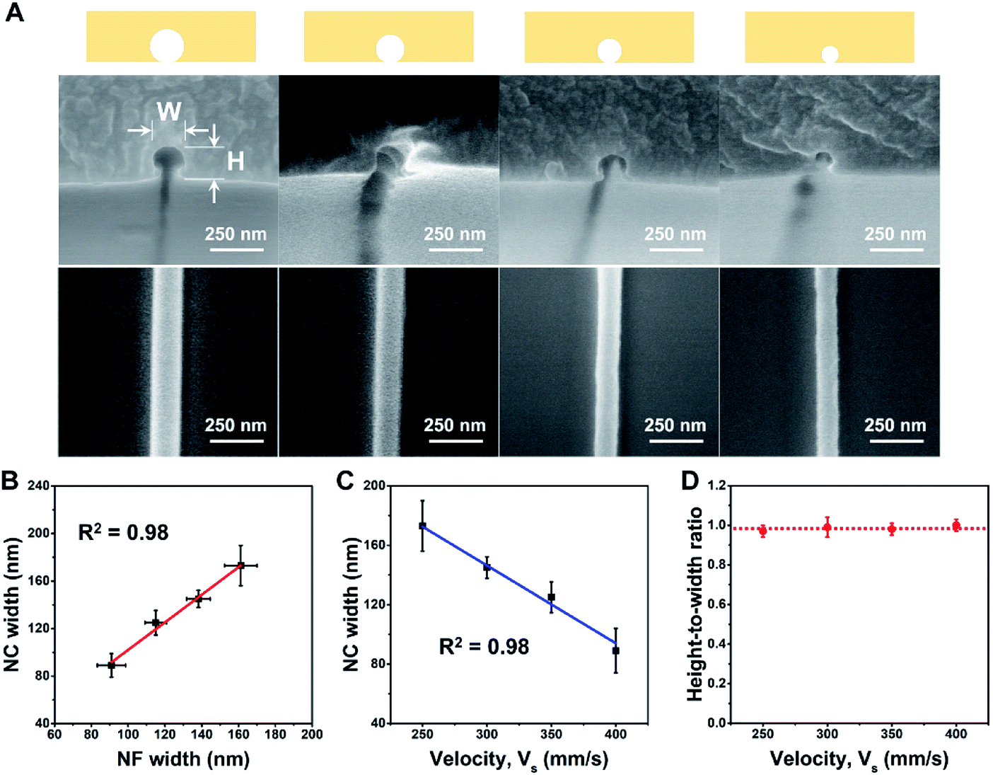 | ||
| Fig. 2 Nanochannels with controlled diameters and fixed circular cross sections. (A) Schematic representations and corresponding SEM images. The nanochannel diameters were varied by manipulating the stage velocity under dry conditions (35 RH%). The corresponding NFs are also shown below the SEM images of the nanochannels. Stage velocities of 250, 300, 350, and 400 mm s−1 (left to right) were employed. (B) An excellent correlation between the NF and nanochannel widths is shown (R2 = 0.98). (C) Linear decrease in the nanochannel diameters upon increasing the stage velocity (R2 = 0.98). (D) The circular cross section is maintained upon controlling the diameter (H and W are indicated in the SEM images of (A)). | ||
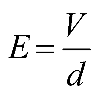
Subsequently, we demonstrated fine control of the cross-sectional shape with various HWRs by adjusting the spinning distance (i.e., 0.5, 0.6, 0.8, 1.0, or 1.2 mm) while maintaining all other operating parameters constant (i.e., stage moving velocity, 400 mm s−1; electric potential, 900 V; and relative humidity, 50 RH%). As the spinning distance affects the evaporation time, the degree of solvent evaporation for the printed NFs can also be influenced as depicted in Fig. 3A. The SEM images of the prepared NFs and the corresponding nanochannels are shown in Fig. 3B, while detailed results are summarized in Table S2 shown in the ESI.† The dimensions in these tables are measured from five different nanochannels, and their coefficients of variation are in the range of 4–20%, which is fairly well controlled compared to those of other nanochannels fabricated using simple methods.32 In addition, as indicated in Fig. 3C, the sizes of the NFs and the obtained nanochannels exhibit a linear relationship (R2 = 0.99). Furthermore, Fig. 3D shows the relationship between the NF width and the spinning distance (0.5–1.2 mm). Moreover, it is noteworthy that the HWR of the channel increases linearly (R2 = 0.97) from 0.19 (semi-ellipsoidal) to 0.96 (circular) upon increasing the spinning distance (Fig. 3E). Indeed, variation in the spinning distance also affected the electric field strength (E), which can be approximated as outlined in eqn (1):
 | (1) |
 | ||
| Fig. 3 Nanochannels with controlled circular cross sections and varying HWRs. (A) Nanochannels with differently shaped cross sections were obtained by varying the spinning distance, thereby resulting in the formation of circular, D-cut, and ellipsoidal cross sections. (B) SEM images of the NFs and the nanochannel cross sections corresponding to the schematic configuration of part (A). Spinning distances of 1.2, 0.8, and 0.6 mm (top to bottom) were employed. (C) An excellent correlation between the NF and nanochannel widths is shown (R2 = 0.99). (D) Variation in the NF width upon altering the spinning distance. (E) Linear relationship between the nanochannel cross section HWR and the spinning distance (H and W are indicated in the SEM images of (B)). (F) Linear relationship between the NF width and the square of the electric field, which is in turn controlled by the spinning distance. | ||
In this context, Fig. 3F shows that the NF width is linearly proportional (R2 = 0.97) to the square of the electric field (E2), which implies that the NF width can be accurately controlled by the electrical force, which in turn can be controlled by the spinning distance. In this case, we found that NF widths of ∼70–368 nm were obtained upon varying the spinning distance between 1.2 and 0.5 mm. As the spinning distance is reduced at a constant applied voltage and a relatively high humidity, the jetting polymer volume is larger due to the increased electric field, thereby resulting in a greater NF width. In addition, the NF comes into contact with the substrate prior to complete evaporation of the solvent, thereby giving an HWR of <1.0 for the NF and yielding nanochannels exhibiting flattened semi-ellipsoidal cross sections. In contrast, with a larger spinning distance, the corresponding electric field is small and the electrospun NF is fully cured prior to coming into contact with the substrate. This gives a nanochannel with small channel width and a circular cross section (HWR ∼1.00).
To confirm the uniformity and the reproducibility of the nanochannel fabrication process, we performed a capillary filling test using nanochannels exhibiting various types of circular cross sections (Fig. 4A). The viscosity of the fluid employed (85 wt% aqueous glycerol) was tuned to reduce the filling velocity and give accurate measurements of its penetration length in the nanochannels, which were recorded using an optical microscope (Fig. 4B, Video S2†). The penetration lengths (l) of the capillary flow showed a highly linear relationship with the square root of the filling time (Fig. 4C), which is predicted by the Lucas–Washburn law. The balance between the capillary suction of a hydrophilic channel and the opposing drag force induced by the fluid viscosity can be expressed by eqn (2) for a nanochannel with an arbitrary cross-sectional shape.57,58
 | (2) |
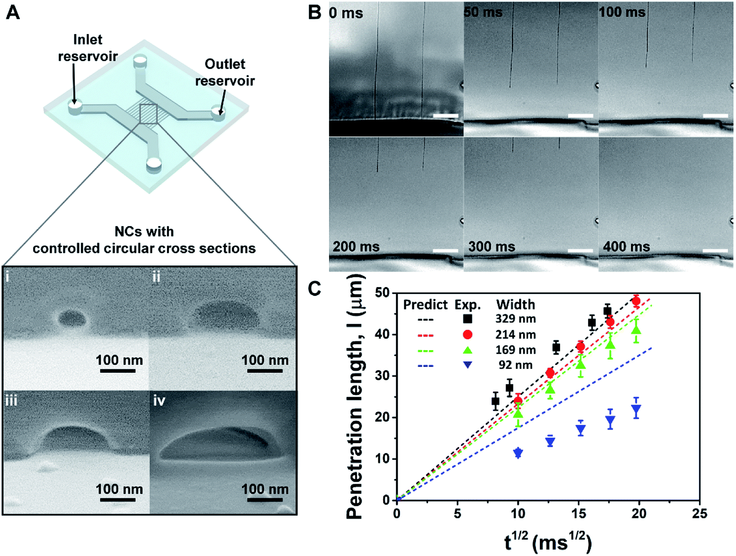 | ||
| Fig. 4 Capillary filling through the nanochannels. (A) Schematic representation of the capillary filling process. Nanochannels with controlled cross-sectional shapes and dimensions are bonded with a glass coverslip using oxygen plasma treatment, and a drop of aqueous glycerol solution is dispensed in the inlet reservoir. (B) Real-time imaging showing penetration of the aqueous glycerol solution through the nanochannels (scale bar = 10 μm). (C) Linear relationship between the position of the liquid meniscus (penetration length of the capillary flow) and the square root of time. For validation, the capillary filling test was conducted using nanochannels with four different HWRs. Average values of the experiments from five nanochannels (n = 5) are plotted. | ||
Conclusions
We herein described a facile nanochannel fabrication method that allows precisely controlling the channel dimensions and the shape of the cross section without requiring a cleanroom process or complex instruments. The obtained polymer-based nanochannels were prepared using sacrificial NF arrays, whose widths and circular cross sections were controlled by manipulating the operating conditions during the NFES step. More specifically, the evaporation rate (humidity), mechanical pulling stress (stage velocity), and electric field (spinning distance) were tuned to prepare custom-designed nanochannels with channel widths ranging from 70 to 368 nm and with either perfect circular cross sections or average HWR values ranging from 0.19 (semi-ellipsoidal) to 0.96 (circular). This simple, low-cost, and high-precision nanochannel fabrication method provides the possibility of large-area mass production, and it is expected to offer greater opportunities to explore the undiscovered unique phenomena and practical applications of nanochannels including further developments in non-lithographic nanopatterning techniques,62,63 ion concentration polarization,64 and nanofluidic diodes.65 It is also promising for use in recently developed biological investigation fields, such as nano flow cytometry66 for extracellular vesicles or tunneling nanotubes,67 which are used for intercellular communication, since the dimensions of the nanochannels can be easily controlled on demand, and the controlled range is comparable to the size of these nanotubes (tens to hundreds of nanometers).Conflicts of interest
There are no conflicts to declare.Acknowledgements
The work was supported by IBS-R020-D1. We are grateful for technical assistance from the staff members, J.-H. Hur at UOBC (UNIST Olympus Biomed Imaging Center) and S. C. Chu at IBS (Institute of Basic Science).References
- L. Wen, Y. Tian, Y. Guo, J. Ma, W. Liu and L. Jiang, Adv. Funct. Mater., 2013, 23, 2887–2893 CrossRef.
- L. Mei, L.-H. Yeh and S. Qian, Nano Energy, 2017, 32, 374–381 CrossRef.
- X. Shang, G. Xie, X.-Y. Kong, Z. Zhang, Y. Zhang, W. Tian, L. Wen and L. Jiang, Adv. Mater., 2017, 29, 1603884 CrossRef PubMed.
- J. Wang, R. Fang, J. Hou, H. Zhang, Y. Tian, H. Wang and L. Jiang, ACS Nano, 2017, 11, 3022–3029 CrossRef PubMed.
- R. Wang, Y. Sun, F. Zhang, M. Song, D. Tian and H. Li, Angew. Chem., Int. Ed., 2017, 129, 1–6 CrossRef.
- Y. Kim, K. S. Kim, K. L. Kounovsky, R. Chang, G. Y. Jung, J. J. dePablo, K. Jo and D. C. Schwartz, Lab Chip, 2011, 11, 1721–1729 RSC.
- E. T. Lam, A. Hastie, C. Lin, D. Ehrlich, S. K. Das, M. D. Austin, P. Deshpande, H. Cao, N. Nagarajan, M. Xiao and P.-Y. Kwok, Nat. Biotechnol., 2012, 30, 771–776 CrossRef PubMed.
- F. I. Uba, S. R. Pullagurla, N. Sirasunthorn, J. Wu, S. Park, R. Chantiwas, Y.-K. Cho, H. Shin and S. A. Soper, Analyst, 2015, 140, 113–126 RSC.
- C. Wang, R. L. Bruce, E. A. Duch, J. V. Patel, J. T. Smith, Y. Astier, B. H. Wunsch, S. Meshram, A. Galan, C. Scerbo, M. A. Pereira, D. Wang, E. G. Colgan, Q. Lin and G. Stolovitzky, ACS Nano, 2015, 9, 1206–1218 CrossRef PubMed.
- A. de la Escosura-Muñiz and A. Merkoçi, Small, 2011, 7, 675–682 CrossRef PubMed.
- A. de la Escosura-Muñiz and A. Merkoçi, ACS Nano, 2012, 6, 7556–7583 CrossRef PubMed.
- R. Wei, V. Gatterdam, R. Wieneke, R. Tampe and U. Rant, Nat. Nanotechnol., 2012, 7, 257–263 CrossRef PubMed.
- K. Shirai, K. Mawatari and T. Kitamori, Small, 2014, 10, 1514–1522 CrossRef PubMed.
- Q. Zhai, S. Zhang, H. Jiang, Q. Wei, E. Wang and J. Wang, J. Mater. Chem. B, 2014, 2, 6371–6377 RSC.
- G. Nie, Y. Sun, F. Zhang, M. Song, D. Tian, L. Jiang and H. Li, Chem. Sci., 2015, 6, 5859–5865 RSC.
- M. Ali, I. Ahmed, P. Ramirez, S. Nasir, C. M. Niemeyer, S. Mafe and W. Ensinger, Small, 2016, 12, 2014–2021 CrossRef PubMed.
- C. Cao, Y.-L. Ying, Z.-L. Hu, D.-F. Liao, H. Tian and Y.-T. Long, Nat. Nanotechnol., 2016, 11, 713–718 CrossRef PubMed.
- R. Peng and D. Li, Nanoscale, 2017, 9, 5964–5974 RSC.
- K. K. Sriram, S. Nayak, S. Pengel, C.-F. Chou and A. Erbe, Analyst, 2017, 142, 273–278 RSC.
- Y. Zhang, R. Zhou, Z. Zhao, X.-Y. Kong, G. Xie, Q. Liu, P. Li, Z. Zhang, K. Xiao, Z. Liu, L. Wen and L. Jiang, ChemPhysChem, 2017, 18, 253–259 CrossRef PubMed.
- S. J. Kim, S. H. Ko, K. H. Kang and J. Han, Nat. Nanotechnol., 2010, 5, 297–301 CrossRef PubMed.
- R. Chantiwas, M. L. Hupert, S. R. Pullagurla, S. Balamurugan, J. Tamarit-Lopez, S. Park, P. Datta, J. Goettert, Y.-K. Cho and S. A. Soper, Lab Chip, 2010, 10, 3255–3264 RSC.
- S. H. Kim, Y. Cui, M. J. Lee, S.-W. Nam, D. Oh, S. H. Kang, Y. S. Kim and S. Park, Lab Chip, 2011, 11, 348–353 RSC.
- J. Wu, R. Chantiwas, A. Amirsadeghi, S. A. Soper and S. Park, Lab Chip, 2011, 11, 2984–2989 RSC.
- Z. Yin, E. Cheng and H. Zou, Lab Chip, 2014, 14, 1614–1621 RSC.
- Y. Ryuji, Y. Yumi, T. Shoji, K. Takahide and F. Hiroyuki, Nanotechnology, 2006, 17, 289–294 CrossRef.
- J. M. Perry, Z. D. Harms and S. C. Jacobson, Small, 2012, 8, 1521–1526 CrossRef PubMed.
- F. Persson, J. Fritzsche, K. U. Mir, M. Modesti, F. Westerlund and J. O. Tegenfeldt, Nano Lett., 2012, 12, 2260–2265 CrossRef PubMed.
- L. D. Menard and J. M. Ramsey, Nano Lett., 2011, 11, 512–517 CrossRef PubMed.
- M. Kim, D. Ha and T. Kim, Nat. Commun., 2015, 6, 6247 CrossRef PubMed.
- Y. Lee, Y. Lim and H. Shin, Nanoscale, 2016, 8, 11810–11817 RSC.
- D. Huh, K. L. Mills, X. Zhu, M. A. Burns, M. D. Thouless and S. Takayama, Nat. Mater., 2007, 6, 424–428 CrossRef PubMed.
- S. Chung, J. H. Lee, M.-W. Moon, J. Han and R. D. Kamm, Adv. Mater., 2008, 20, 3011–3016 CrossRef.
- K. L. Mills, D. Huh, S. Takayama and M. D. Thouless, Lab Chip, 2010, 10, 1627–1630 RSC.
- S. Nagashima, H. Ebrahimi, K.-R. Lee, A. Vaziri and M.-W. Moon, Adv. Mater. Interfaces, 2015, 2, 1400493 CrossRef.
- S.-m. Park, Y. S. Huh, H. G. Craighead and D. Erickson, Proc. Natl. Acad. Sci. U.S.A., 2009, 106, 15549–15554 CrossRef PubMed.
- J. Heo, H. J. Kwon, H. Jeon, B. Kim, S. J. Kim and G. Lim, Nanoscale, 2014, 6, 9681–9688 RSC.
- D. A. Czaplewski, J. Kameoka, R. Mathers, G. W. Coates and H. G. Craighead, Appl. Phys. Lett., 2003, 83, 4836–4838 CrossRef.
- S. S. Verbridge, J. B. Edel, S. M. Stavis, J. M. Moran-Mirabal, S. D. Allen, G. Coates and H. G. Craighead, J. Appl. Phys., 2005, 97, 124317 CrossRef.
- L. M. Bellan, E. A. Strychalski and H. G. Craighead, J. Vac. Sci. Technol., B, 2008, 26, 1728–1731 Search PubMed.
- C. Kyo Seon, K. Seungwook, C. Haegeun, O. Joon-Ho, S. Tae-Yeon, A. Boo Hyun, K. Young Keun, P. Jae Hyoung, D. Young Rag and K. Woong, Nanotechnology, 2010, 21, 425302 CrossRef PubMed.
- G. Weiwei, X. Jiongwei, Z. Qianwei, W. Xiudong and X. Shengyong, Nanotechnology, 2010, 21, 195302 CrossRef PubMed.
- P. Sivanesan, K. Okamoto, D. English, C. S. Lee and D. L. DeVoe, Anal. Chem., 2005, 77, 2252–2258 CrossRef PubMed.
- D. Li and Y. Xia, Nano Lett., 2004, 4, 933–938 CrossRef.
- M. Wang, N. Jing, C. B. Su, J. Kameoka, C.-K. Chou, M.-C. Hung and K.-A. Chang, Appl. Phys. Lett., 2006, 88, 033106 CrossRef.
- B. Zhang, M. Wood and H. Lee, Anal. Chem., 2009, 81, 5541–5548 CrossRef PubMed.
- W. Chee Chung, A. Ajay, N. Balasubramanian and K. Dim Lee, Nanotechnology, 2007, 18, 135304 CrossRef PubMed.
- A. Agarwal, N. Ranganathan, W.-L. Ong, K. C. Tang and L. Yobas, Sens. Actuators, A, 2008, 142, 80–87 CrossRef.
- Y. Liu and L. Yobas, Biomicrofluidics, 2012, 6, 046502 CrossRef PubMed.
- D. Sun, C. Chang, S. Li and L. Lin, Nano Lett., 2006, 6, 839–842 CrossRef PubMed.
- G. S. Bisht, G. Canton, A. Mirsepassi, L. Kulinsky, S. Oh, D. Dunn-Rankin and M. J. Madou, Nano Lett., 2011, 11, 1831–1837 CrossRef PubMed.
- C. Chang, K. Limkrailassiri and L. Lin, Appl. Phys. Lett., 2008, 93, 123111 CrossRef.
- Y. Huang, Y. Duan, Y. Ding, N. Bu, Y. Pan, N. Lu and Z. Yin, Sci. Rep., 2014, 4, 5949 CrossRef PubMed.
- Y. Huang, N. Bu, Y. Duan, Y. Pan, H. Liu, Z. Yin and Y. Xiong, Nanoscale, 2013, 5, 12007–12017 RSC.
- N. Bu, Y. Huang, X. Wang and Z. Yin, Mater. Manuf. Processes, 2012, 27, 1318–1323 CrossRef.
- C.-H. Chen, in Electrokinetics and Electrohydrodynamics in Microsystems, ed. A. Ramos, Springer Vienna, Vienna, 2011, vol. 6, pp. 177–220, DOI:10.1007/978-3-7091-0900-7.
- M. Pliego, G. J. Gutiérrez and A. Medina, Rev. Mex. Fis., 2011, 57, 1–5 Search PubMed.
- J. M. Oh, T. Faez, S. de Beer and F. Mugele, Microfluid. Nanofluid., 2010, 9, 123–129 CrossRef.
- N. V. Churaev, V. D. Sobolev and Z. M. Zorin, Special Discussion on Thin Liquid Films and Boundary Layers, Academic, New York, 1971 Search PubMed.
- N. R. Tas, J. Haneveld, H. V. Jansen, M. Elwenspoek and A. v. d. Berg, Appl. Phys. Lett., 2004, 85, 3274–3276 CrossRef.
- J. Haneveld, N. R. Tas, N. Brunets, H. V. Jansen and M. Elwenspoek, J. Appl. Phys., 2008, 104, 014309 CrossRef.
- P. Kumar, M. G. Krishna, A. K. Bhatnagar and A. K. Bhattacharya, Int. J. of Nanomanufacturing, 2008, 2, 477–495 CrossRef.
- P. Kumar, J. Nanopart. Res., 2010, 12, 2473–2480 CrossRef.
- C. Chih-Chang, Y. Cheng-Peng and Y. Ruey-Jen, Electrophoresis, 2012, 33, 758–764 CrossRef PubMed.
- P. Ramirez, V. Garcia-Morales, V. Gomez, M. Ali, S. Nasir, W. Ensinger and S. Mafe, Phys. Rev. Appl., 2017, 7, 064035 CrossRef.
- R. Friedrich, S. Block, M. Alizadehheidari, S. Heider, J. Fritzsche, E. K. Esbjorner, F. Westerlund and M. Bally, Lab Chip, 2017, 17, 830–841 RSC.
- M. W. Austefjord, H.-H. Gerdes and X. Wang, Commun. Integr. Biol., 2014, 7, e27934 CrossRef PubMed.
Footnote |
| † Electronic supplementary information (ESI) available. See DOI: 10.1039/c8ra03496f |
| This journal is © The Royal Society of Chemistry 2018 |