
 Open Access Article
 This Open Access Article is licensed under a
 Creative Commons Attribution 3.0 Unported Licence
Synthesis of silver sulfide nanoparticles and their photodetector applications†
Myung Hyun Kanga,
Sung Ho Kima,
Seunghun Jangb,
Ji Eun Lima,
Hyunju Changb,
Ki-jeong Kongb,
Sung Myung *a and
Joung Kyu Park*a
*a and
Joung Kyu Park*a
aAdvanced Materials Division, Korea Research Institute of Chemical Technology, Daejeon, Korea. E-mail: parkjk@krict.re.kr
bCenter for Molecular Modeling and Simulation, Korea Research Institute of Chemical Technology, Daejeon, Korea
First published on 9th August 2018
Abstract
Silver sulfide nanoparticles (Ag2S NPs) are currently being explored as infrared active nanomaterials that can provide environmentally stable alternatives to heavy metals such as lead. In this paper, we describe the novel synthesis of Ag2S NPs by using a sonochemistry method and the fabrication of photodetector devices through the integration of Ag2S NPs atop a graphene sheet. We have also synthesized Li-doped Ag2S NPs that exhibited a significantly enhanced photodetector sensitivity via their enhanced absorption ability in the UV-NIR region. First-principles calculations based on a density functional theory formalism indicated that Li-doping produced a dramatic enhancement of NIR photoluminescence of the Ag2S NPs. Finally, high-performance photodetectors based on CVD graphene and Ag2S NPs were demonstrated and investigated; the hybrid photodetectors based on Ag2S NPs and Li-doped Ag2S NPs exhibited a photoresponse of 2723.2 and 4146.0 A W−1 respectively under a light exposure of 0.89 mW cm−2 at 550 nm. Our novel approach represents a promising and effective method for the synthesis of eco-friendly semiconducting NPs for photoelectric devices.
Introduction
Ultraviolet (UV), visible, and near infrared (NIR) imaging with nanoparticles (NPs) has been extensively investigated owing to their utility in many applications, such as electroluminescent devices, optical modulators, photodetectors, and biological fluorophores.1–9 Recently, quantum dot NPs, such as PbS and PbSe, have particularly emerged as some of the most promising new materials for the development of advanced photoelectric devices, because of low-cost manufacturing, solution processability, and their superior photoelectric properties including unique absorption and emission of light in the NIR regions.10–15 However, lead-containing NPs are highly toxic and responsible for extensive environmental contamination and health problems in various parts of the world.16,17 In order to overcome these limitations, the Ag2S NPs have been extensively studied as attractive NIR-absorbing NPs for photovoltaics, photoconductors, and IR detectors due to their high biocompatibility and unique absorption ability in the UV-NIR regions, which can be used as multispectral photodetectors in UV, visible, and NIR spectrum because of their light absorption in a broad wavelength range.18–27 However, the development of a facile and easy methods for the preparation of the high-quality and monodisperse Ag2S NPs is still required for routine industrial applications including photoelectric devices and photodetectors.In this study, we demonstrate the facile preparation of Ag2S NPs and one-pot synthesis of Li-doped Ag2S NPs via ultrasonic irradiation, which resulted in a dramatic enhancement of their absorption and emission capabilities in the NIR region. The effect of Li ion doping on the electronic structure of the Ag2S system was also investigated by first-principles calculations, which indicated that the Li-doped Ag2S NPs could enhance the photoluminescence of semiconducting nanocrystals. Finally, hybrid photodetectors based on transparent CVD graphene nanosheets and Ag2S NPs were successfully fabricated. These photodetectors based on pristine Ag2S NPs and Li-doped Ag2S NPs showed photoresponses of 2723.2 and 4146.0 A W−1, respectively, under a light exposure of 0.89 mW cm−2 at 550 nm. The proposed synthesis and doping methods constitute a facile and efficient approach for fabricating graphene-NP-based hybrid two-dimensional (2D) photoelectric devices for various applications, including flexible devices and advanced photo-transistors.
Results and discussion
The facile synthesis of 10 nm Ag2S NPs was performed by using a sonochemical method, in which the decomposition of raw materials is induced by ultrasound under ambient conditions (Fig. 1a). Silver nitrate (AgNO3) in 1-dodecanethiol was sonicated to generate localized hot spots within the acoustic cavitation of collapsing bubbles during ultrasonic irradiation (reaction time: 10 min, power: 50%, temperature: ∼160 °C) (see Fig. S1 in ESI †). In order to improve NIR photodetector sensitivity, Li-doped Ag2S NPs were also synthesized using a method similar to that used for pristine Ag2S NPs by adding the appropriate amount of Li in the reaction bottle (Fig. 1b). Such photosensitive materials can lead to an enhancement of the absorption ability in the broad wavelength range, resulting in an overall improvement of their photodetector performance. | ||
| Fig. 1 Synthesis of Ag2S NPs and Li-doped Ag2S NPs. Schematic illustration of the synthesis of (a) Ag2S NPs and (b) Li-doped Ag2S NPs by using ultrasonic irradiation. | ||
Transmission electron microscopy (TEM) analysis was used to characterize the structure and morphology of Ag2S NPs and Li-doped Ag2S NPs. The TEM images of the as-prepared Ag2S NPs confirmed the monodispersity and narrow size distribution of the NPs (Fig. 2a) that can be attributed to the effective separation of the nucleation and growth processes during ultrasonic irradiation at 160 °C. This result was similar to that reported in a previous study.28
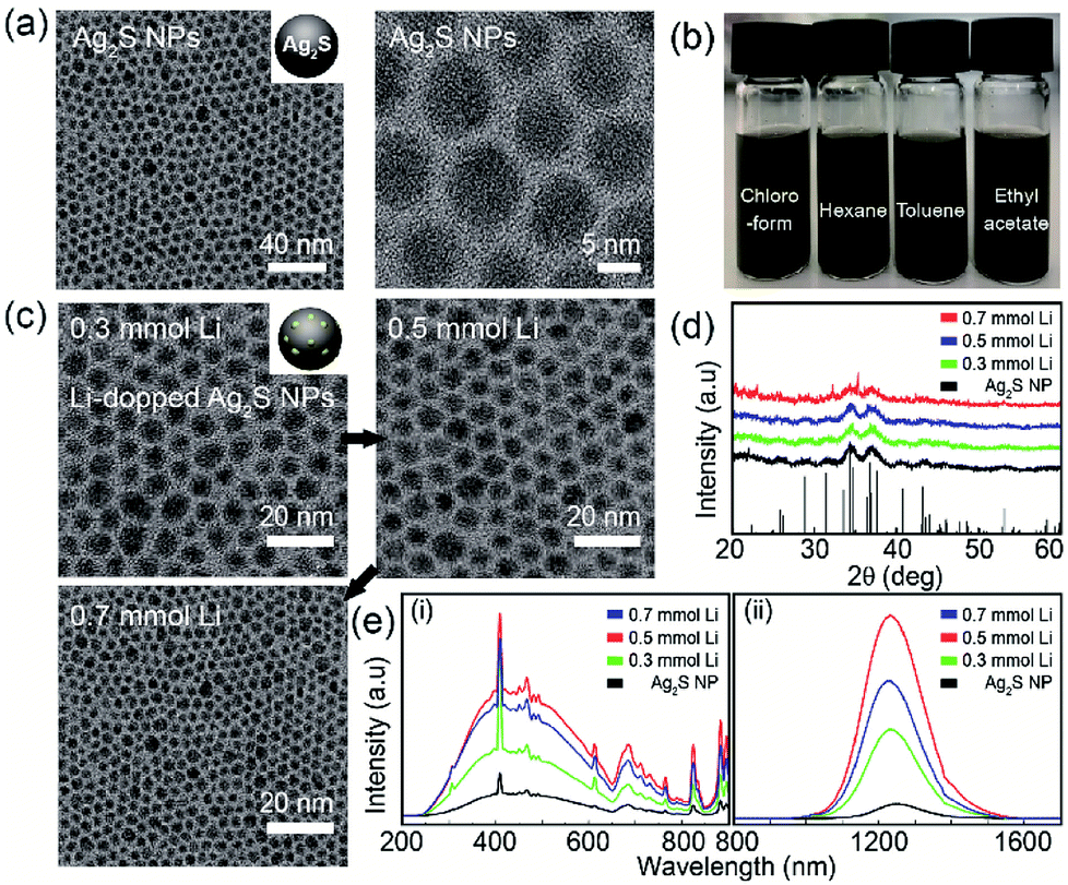 | ||
| Fig. 2 Synthesis of Ag2S NPs and Li-doped Ag2S NPs. (a) Representative TEM images of Ag2S NPs with a 10 nm size. (b) Optical images of the dispersion of Ag2S NPs in chloroform, hexane, toluene, and ethyl acetate. (c) XRD patterns of Ag2S NPs in terms of Li concentrations. (d) TEM images for 0.3 mmol Li-doped (right), 0.5 mmol Li doped (middle), and 0.7 mmol Li-doped (left) Ag2S NPs. (e) UV-Vis-NIR absorption spectra (left) and PL emission spectra under an excitation of 850 nm (right). | ||
Significantly, the Ag2S NPs were well dispersed in various organic solvents due to the presence of dodecanethiol coated on the NP surface (Fig. 2b). In the XRD patterns of the Ag2S NPs doped with different amounts of Li+, most of the peaks corresponded to the monoclinic Ag2S phase (JCPDS no. 014-0072) (Fig. 2d). The TEM images of Li-doped Ag2S NPs for different Li+ amounts revealed spherical monodisperse NPs; Li contents did not affect particle morphology and size (Fig. 2c). The photoluminescence (PL) excitation and emission spectra of Ag2S NPs as a function of the Li concentration are shown in Fig. 2e. Unlike general quantum dots, involving PbSe and PbS, these NPs could be effectively excited across the UV-NIR region (See Fig. S2 in ESI†). It has been reported that the Ag2S NPs emits efficiently under the various excitation ranges, which makes them promising candidates for photodetectors requiring unique absorption in the various wavelength regions (from UV to NIR). As the content of Li+ increased, the emission intensities of the Ag2S NPs increased up to 0.05 mmol and exhibited an emission peak at 1250 nm (Fig. 2e). The Li-doped Ag2S NPs were found to display a remarkable enhancement of the emission intensity (up to two orders) compared to that of the undoped Ag2S NPs. It is well known that even at very small concentrations, Li+ ions play an important role as co-dopants in increasing the luminescent efficiency of phosphors.28 In the XPS spectrum, only Ag and S peaks are observed and Li 1S peak is unable to distinguish with Ag 4P at around 55 eV because Li 1S peak and Ag 4P peak overlap each other (see Fig. S3 in ESI †). But ICP analysis confirmed the existence of Li in these Ag2S NPs (see Fig. S4 in ESI †).
To understand the effect of Li ion doping on the electronic structures of the Ag2S system, we performed first-principles calculations based on the density functional theory formalism for the Li interstitials and substitutions in crystalline Ag2S. Fig. 3 (left) shows the optimized atomic geometries of (a) 3 × 2 × 1 Ag2S supercell (321-pristine), (c) 3 × 2 × 1 Ag2S supercell with a Li interstitial (321-Lii-1), and (e) 3 × 2 × 1 Ag2S supercell with two Li interstitials (321-Lii-2near). As shown in Fig. 2d, since the Li contents did not affect the structural properties of Ag2S NPs, not only interstitial doping but also substitution were considered in our calculations. The Li concentration was about 0.12 wt% for the case of 321-Lii-1, which corresponded to the experimental conditions. Although a Li interstitial was added in the interspace of the Ag2S cell, its crystal structure was well preserved, as shown in Fig. 3c. Furthermore, when an additional Li atom was appended, a local amorphous structure in the doped Ag2S began to appear (Fig. 3e). Additionally, the calculations for the Li substitutions at the Ag sites in the 3 × 2 × 1 A Ag2S supercell were also carried out (See Fig. S5 in ESI†).
 | ||
| Fig. 3 Calculations for the pristine and Li doped (interstitials) 3 × 2 × 1 Ag2S. Calculated optimized atomic geometries for the (a) 321-pristine, (c) 321-Lii-1, and (e) 321-Lii-2near. The gray, yellow, and green balls represent the Ag, S, and Li atoms, respectively. Calculated band structures and PDOSs for (b) 321-pristine, (d) 321-Lii-1, and (f) 321-Lii-2near. The Fermi levels of all calculated systems were set at zero. | ||
Since Li+ ions (0.9 Å) have a smaller ionic radius than Ag+ ions (1.3 Å) in the Ag2S crystal, regardless of the number (per unit-cell) of Li substitutions, the crystal structures of doped Ag2S systems with Li substitutions at the Ag sites were well maintained.29 Likewise, the electronic structure of Ag2S hardly changed upon Li substitution (See Fig. S5 in ESI†). However, the Li interstitial in the Ag2S crystal caused a significant change in the electronic structure. Fig. 3 (right) shows the calculated band structures and projected density of states (PDOS) of (b) 321-pristine, (d) 321-Lii-1, and (f) 321-Lii-2near. As shown in the band structures of Fig. 3b and d, the bottom of the conduction band shifted below the Fermi level by the Li interstitial doping. As a result, 321-Lii-1 exhibited a metallic band gap. The Li impurity provides a partial 2s electron to the pristine Ag2S system, which leads the change in band structure from a semiconducting to a metallic band gap.30
In the case of the 321-Lii-2near system with two Li interstitials, it could be confirmed that the bottom of the conduction band was reduced to a lower energy level than that of 321-Lii-1 by an additional Li 2 s partial electron (Fig. 3d and f). In order to check the effect of the Li–Li interaction on the electronic structure of the Li doped-Ag2S system, the calculations for the 3 × 2 × 1 Ag2S supercells with two Li interstitials (or two Li substitutions) were performed by varying the Li–Li interdistance (See Fig. S6 or S5c–f in ESI†). However, no noticeable influence of the electronic structure on the interaction between two Li interstitials (or two Li substitutions) in the Ag2S system was observed.
Based on the results obtained from our calculations, we proposed the following mechanism for the photoluminescence enhancement and quenching in Fig. 2e, as shown in Fig. 4. Extra carriers in Li interstitial doped Ag2S are accumulated within the crystal, which further enhances its metallic property. By increasing the Li doping concentration, extra electrons in metallic NPs begin to migrate to original semiconducting NP outside (Step 2 in Fig. 4), thus positively charged metallic NPs can enhance the photoluminescence of the semiconducting NPs.
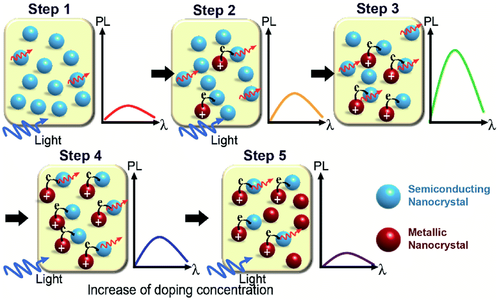 | ||
| Fig. 4 Mechanism of photoluminescence enhancement and quenching Li-doped Ag2S NPs. Schematic diagram for the mechanism of the photoluminescence enhancement and quenching in Li-doped Ag2S NPs by increasing Li doping concentration (from Step 1 to Step 5, along the black arrow direction). The blue-sky and red balls represent the semiconducting and metallic Ag2S NP. The blue and red wave arrows indicate the photoluminescence excitation source and light emission, respectively. | ||
However, this phenomenon takes place only up to optimal doping conditions (Step 3 in Fig. 4). Above a certain doping concentration, the absolute number of semiconducting NPs participating in the photoluminescence process are reduced compared to that of metallic NPs, and thereby the total luminescence of the sample begins to decrease rather than increase (from Step 4 to Step 5 in Fig. 4). A similar mechanism of photoluminescence enhancement and quenching has been already proposed in a previous study on Ag-doped CdSe NP.31
In addition, Ag2S NPs and Li-doped Ag2S NPs were successfully employed for the fabrication of hybrid photodetectors based on CVD graphene and photosensitive NPs. Recently, carbon-based materials, such as carbon nanotubes, graphene oxide, and graphene have drawn considerable attention due to their superior optical, electrical, and mechanical properties.32 Among carbon materials, graphene and graphene-related materials have been proposed as strong candidates for various optoelectronic applications, such as ultra-broadband photodetectors and solar cells.33 However, their low optical absorption and the short recombination rate have limited their application to graphene-based optoelectronic devices. First, 1-octadecyltrichlorosilane (OTS) was utilized as self-assembled monolayer (SAM) molecules to achieve the uniform assembly of Ag2S NPs. In this case, a UV/ozone treatment of the SiO2 surface was carried out, and the UV-treated SiO2 substrate was placed in the OTS solution to cover the SiO2 surface. When the OTS-coated SiO2 substrate was placed in the solution of methyl-terminated Ag2S NPs, the Ag2S NPs were assembled on the neutral-charged OTS molecular layer. CVD-grown graphene nanosheets were transferred on the top of Ag2S NPs using a PMMA-assisted wet transfer method. Finally, Au/Cr acting as source and drain electrodes were deposited using a shadow mask, while 1-butyl-3-methylimidazolium (BmimPF6) was used as the ionic liquid. Ag2S NPs were used as photosensitive materials. As shown in the image in Fig. 5a, the channel length and width of the device were 100 μm and 500 μm, respectively. The SEM image in Fig. 5a and atomic force microscopy (AFM) image showed that the NP density on the SiO2 substrate was uniform (See Fig. S8 in ESI†), and the NP density was approximately 150 μm−2. The transfer curve (IDS–VG) of pristine graphene devices at VDS = 0.1 V exhibited a charge-neutral Dirac point at a near-zero gate voltage (VG) and an asymmetric hole and electron conduction (see Fig. S9 in ESI†). In the case of devices based on Ag2S NPs and graphene, the Dirac voltage showed a positive shift compared with that of pristine graphene devices, and this positive shift was increased with increase of the illumination power. The electrical band structures provide a good explanation of the difference between the photodetectors based on graphene and Ag2S NPs, as shown in Fig. 5c. The energy-band bending at the interface between a surface of graphene and Ag2S NPs also occurred. The direction of the built-in electric field was formed from the graphene to the Ag2S NPs. The photo-generated electrons (or holes) in the Ag2S NPs moved within the graphene sheet with the passage of the energy band bending at the interface under the light illumination.34–36 The photodetector showed an increase of current level under the exposure to a light source. Here, holes transfer from Ag2S NPs to graphene resulted in an increase in the photocurrent (Fig. 5c). Fig. 5d shows the Ag2S-graphene photodetector under a light exposure of 0.00, 0.23, 0.38, 0.50, 0.76, and 0.89 mW cm−2 exhibited a Dirac voltage of 2.2, 2.4, 2.6, 2.9, 3.0 and 3.5 V, respectively.
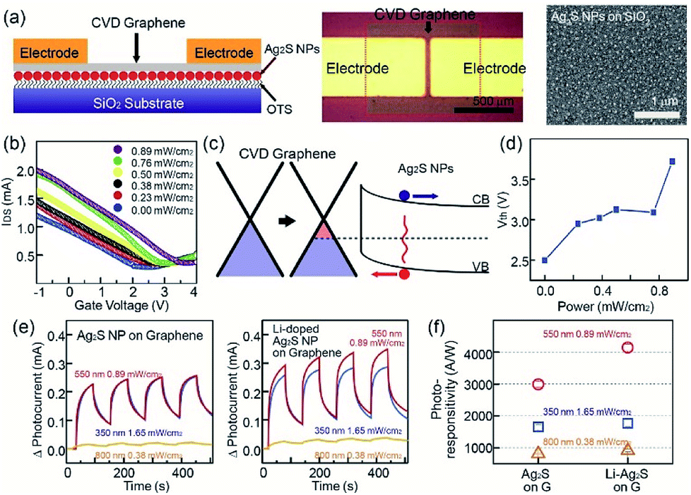 | ||
| Fig. 5 Photodetectors based on graphene and Ag2S NPs (a) a schematic diagram of the structure of a photodetector based on graphene and Ag2S NPs (left). Optical image of the photodetectors (middle). SEM image of graphene on Ag2S NPs (right). (b) The transfer characteristics of a transistor based on graphene and Ag2S NPs under various light exposing conditions. (c) A schematic energy band diagram of the Fermi level variation of graphene and Ag2S NPs. (d) Threshold voltage of the devices as a function of light power. (e) Photocurrent of photodetector based graphene-Ag2S NPs (left) and graphene Li-doped Ag2S NPs (right) under cyclic light exposure. Here, a light source of 0.89 W m−2 at 550 nm, 1.65 W m−2 at 350 nm, and 0.38 W m−2 at 800 nm was used for the measurements. (f) Photoresponsitivity of photodetectors based graphene-Ag2S NPs and graphene Li-doped Ag2S NPs obtained by light exposure of 0.89 W m−2 at 550 nm, 1.65 W m−2 at 350 nm, and 0.38 W m−2 at 800 nm. | ||
The photoresponse characteristics of hybrid photodetectors were evaluated by measuring the time-dependent photocurrent under various illumination conditions, such as 0.89 W m−2 at 550 nm, 1.65 W m−2 at 350 nm, and 0.38 W m−2 at 800 nm. First, in the case of photodevices based on pristine Ag2S NPs, the current through the graphene channel increased under light exposure. Moreover, we observed that the photocurrent under the light exposure at 350- and 550 nm wavelengths was larger than that under 800 nm, as shown in Fig. 5e. In addition, as previously mentioned, Li-doped Ag2S NPs possess superior light absorption properties than pristine Ag2S NPs, while photodetectors based on graphene and Ag2S NPs exhibit a larger photocurrent than Ag2S NPs. Fig. 5f shows the photoresponse of our devices under the various exposing conditions. For example, hybrid photodetectors based on Ag2S NPs and Li-doped Ag2S NPs displayed a photoresponse of 2723.2 and 4146.0 A W−1, respectively, under a light exposure of 0.89 mW cm−2 at 550 nm. In order to investigate the stability of the NPs, the photo and thermal stability of NPs was studied by illuminating the NPs using UV (365 nm) and heat-treated temperatures for various times. The PL emission intensities of the samples does not show much reduction in PL emission intensities, which shows the NPs have high photo and thermal stability. Moreover, to investigate the long-term air-stability, graphene photodetectors with based a graphene transistor with Ag2S NPs and Li-doped Ag2S NPs were placed in an environmental chamber, with a relative humidity and temperature of 50% and 25 °C, respectively. Our photodetectors exhibited a similar trend with NPs data for 90 days, possibly due to charge trapping from water molecules on the graphene surface, which shows high reliability and stability of the NPs as well as photodetector devices (see Fig. S10 and S11 in ESI†).
Experimental
Materials
Silver nitrate (AgNO3, 99%), Li2CO3 (98%), and 1-dodecanethiol (DDT) were purchased from Sigma Aldrich. Chloroform and ethyl acetate were used to disperse and to isolate the NPs. All chemicals were used without further purification.Synthesis of Ag2S NPs and Li-doped Ag2S NPs
The Ag2S and Li-doped Ag2S NPs were synthesized by ultrasonication. For the synthesis of Ag2S NPs, AgNO3 was added to a 20 mL vial containing 10 mL of DDT. The solution was treated by ultrasound irradiation for 10 min in air atmosphere. The resulting suspension was centrifuged with ethyl acetate several times to remove any by-products and dried in an electric oven at 80 °C. The Li-doped Ag2S NPs were synthesized in the same way, upon addition of the appropriate amount of lithium to the reaction bottle.Characterization of Ag2S and Li-doped Ag2S NPs
The absorption spectra of solutions containing 0.01 g of Ag2S and Li-doped Ag2S NPs (in 10 mL of chloroform) were measured using a SolidSpec-3700 UV-Vis-NIR spectrophotometer from Shimadzu. The photoluminescence (PL) spectra were measured by a Fluorolog3 with TCSPC mode (HORIBA Scientific). All samples were excited by a CW 450 W xenon source, and directed to a single-grating spectrometer. The PL spectra were obtained using a InP/InGaAs detector equipped with an LN cooler. All TEM images were acquired on a JOEL JEM-2100F transmission electron microscope operating at 200 KV. The TEM samples were prepared by drop-casting very thin nanoparticle solutions onto a 200 mesh copper grid with a carbon film (Ted Pella). X-ray diffraction spectroscopy (XRD) for the NPs was performed using a Rigaku D/MAX-220 V X-ray diffractometer equipped with Cu K-alpha (1.540598 Å) source.Computational details
The atomic and electronic structures of the pristine and Li-doped Ag2S systems were examined using the Vienna ab initio simulation package (VASP).37,38 The exchange correlation functional was approximated using the PBEsol (Perdew–Burke–Ernzerhof revised for solids) expression.39 The electron–ion interactions were modeled using the projector augmented wave (PAW) method.40 The electronic wave functions were expanded in a basis set of plane waves using a kinetic energy cutoff of 500 eV. Geometry relaxation steps were performed under the criterion that ionic forces were reduced below 0.02 eV Å−1. Doped Ag2S systems with interstitial and substitutional Li atoms were analyzed using a unit cell (1 × 1 × 1) and 3 × 2 × 1 supercells with 10 × 5 × 5 and 4 × 3 × 5 k-point meshes, respectively. The crystal data of β-Ag2S were consistent with earlier reports and were used as the lattice parameters of the pristine Ag2S system in this work.41,42 The pristine Ag2S system possessed a monoclinic crystal structure (space group P21/c, a = 4.231 Å, b = 6.930 Å, c = 9.526 Å, β = 125.48°), as shown in Fig. S7a in ESI.†Fabrication of photodetectors based on Ag2S (or Li-doped Ag2S NPs) and graphene
First, a SiO2 surface was subjected to a UV/ozone treatment at atmospheric pressure, and then the UV-treated SiO2 substrate was placed in an OTS solution (1/500 by volume ratio in anhydrous hexane). After the OTS-coated SiO2 substrate was placed in a 0.16 wt% solution of Ag2S NPs and Li-doped Ag2S (total solution of 0.1 g NPs under 50 mL CHCl3) usually for about 5 minutes, the Ag2S NPs were assembled on the OTS molecular layer. CVD-grown graphene nanosheets were transferred on top of the Ag2S NPs using a PMMA-assisted wet transfer method. Au/Cr (as source/drain electrodes) were deposited using a shadow mask. In our study, Cr (7 nm)/Au (70 nm), 1-butyl-3-methylimidazolium, and Ag2S NPs were used as the source/drain electrodes, ionic liquid, and photosensitive materials, respectively.Conclusion
In summary, the facile preparation of Ag2S NPs and Li-doped Ag2S NPs was successfully achieved for the development of high-performance optoelectronic devices. These materials showed enhancements of absorption and emission in the NIR region through a one-step process upon ultrasonic irradiation. The effect of Li ion doping on the electronic structure of the Ag2S was also investigated by first-principles calculations, which indicated that the Li-doped Ag2S NPs could have enhanced the NIR photoluminescence and absorption abilities.Finally, hybrid photodetectors based on transparent CVD graphene nanosheets and Ag2S NPs were successfully fabricated. These photodetectors based on pristine Ag2S NPs and Li-doped Ag2S NPs showed photoresponses of 2723.2 and 4146.0 A W−1, respectively, under a light exposure of 0.89 mW cm−2 at 550 nm. This approach provides a facile high-quality synthesis method for NPs as well as a doping method for the fabrication of advanced hybrid photoelectric devices such as advanced photo-transistors, and solar cells.
Conflicts of interest
There are no conflicts to declare.Acknowledgements
M. H. K., S. H. K., and S. J. contributed equally to this work. This research was funded by the Korean Ministry of Science and Technology through KK-1607-C11, BS.K18M201, KNI1801, IJ17-05, IJ18-07, KK1802-C00. This research was also supported by Nano/Material Technology Development Program through the National Research Foundation of Korea (NRF) funded by the Ministry of Education, Science and Technology (NRF-2017M3D9A1073502).Notes and references
- F. Guo, B. Yang, Y. Yuan, Z. Xiao, Q. Dong, Y. Bi and J. Huang, Nat. Nanotechnol., 2012, 7, 798–802 CrossRef PubMed.
- K. Liu, M. Sakurai and M. Aono, Sensors, 2010, 10, 8604–8634 CrossRef PubMed.
- G. Konstantatos, J. Clifford, L. Levina and E. Sargent, Nat. Photonics, 2007, 1, 531–534 CrossRef.
- S. W. Shin, K. H. Lee, J. S. Park and S. J. Kang, ACS Appl. Mater. Interfaces, 2015, 7, 19666–19671 CrossRef PubMed.
- E. H. Sargent, Adv. Mater., 2005, 17, 515–522 CrossRef.
- N. Tessler, V. Medvedev, M. Kazes, S. Kan and U. Banin, Science, 2002, 295, 1506–1508 CrossRef PubMed.
- L. Bakueva, G. Konstantats, L. Levina, S. Musikhin and E. H. Sargent, Appl. Phys. Lett., 2004, 84, 3459–3461 CrossRef.
- B. L. Wehrenberg and P. Guyot-Sionnest, J. Am. Chem. Soc., 2003, 125, 7806–7807 CrossRef PubMed.
- X. Gao, Y. Cui, R. M. Levenson, L. W. K. Chung and S. Nie, Nat. Biotechnol., 2004, 22, 969–976 CrossRef PubMed.
- R. Saran and R. J. Curry, Nat. Photonics, 2016, 10, 81–92 CrossRef.
- G. Konstantatos, I. Howard, A. Fischer, S. Hoogland, J. Clifford, E. Klem, L. Levina and E. H. Sargent, Nature, 2006, 442, 180–183 CrossRef PubMed.
- S. A. Mcdonald, Nat. Mater., 2005, 4, 138–142 CrossRef PubMed.
- G. Konstantatos and E. H. Sargent, Nat. Nanotechnol., 2010, 5, 391–400 CrossRef PubMed.
- K. Szendrei, F. Cordella, M. V. Kovalenko, M. Böberl, G. Hesser, M. Yarema, D. Jarzab, O. V. Mikhnenko, A. Gocalinska, M. Saba, F. Quochi, A. Mura, G. Bongiovanni, P. W. M. Blo, W. Heiss and M. A. Loi, Adv. Mater., 2009, 21, 683–687 CrossRef.
- M. Böberl, M. V. Kovalenko, S. Gamerith, E. J. W. List and W. Heiss, Adv. Mater., 2007, 19, 3574–3578 CrossRef.
- Y. Cao, H. Liu, Q. Li, Q. Wang, W. Zhang, Y. Chen, D. Wang and Y. Cai, J. Inorg. Biochem., 2013, 126, 70–75 CrossRef PubMed.
- Q. Li, X. Hu, Y. Bai, M. Alattar, D. Ma, Y. Cao, Y. Hao, L. Wang and C. Jiang, Food Chem. Toxicol., 2013, 60, 213–217 CrossRef PubMed.
- Y. Zhang, G. Hong, Y. Zhang, G. Chen, F. Li, H. Dai and Q. Wang, ACS Nano, 2012, 6, 3695–3702 CrossRef PubMed.
- Y. Zhang, Y. Zhang, G. Hong, W. He, K. Zhou, K. Yang, F. Li, G. Chen, Z. Liu, H. Dai and Q. Wang, Biomaterials, 2013, 34, 3639–3646 CrossRef PubMed.
- C. Li, Y. Zhang, M. Wang, Y. Zhang, G. Chen, L. Li, D. Wu and Q. Wang, Biomaterials, 2014, 35, 393–400 CrossRef PubMed.
- E. Cassette, M. Helle, L. Benzdetnaya, F. Marchal, B. Dubertret and T. Pons, Adv. Drug Delivery, 2013, 65, 719–731 CrossRef PubMed.
- G. Chen, F. Tian, Y. Zhang, Y. Zhang, C. Li and Q. Wang, Adv. Funct. Mater., 2014, 24, 2481–2488 CrossRef.
- P. Jiang, C. Zhu, Z. Zhang, Z. Tian and D. Pang, Biomaterials, 2012, 33, 5130–5135 CrossRef PubMed.
- S. S. Dhumure and C. D. Lokhande, Sol. Energy Mater. Sol. Cells, 1992, 28, 159–166 CrossRef.
- S. S. Dhumure and C. D. Lokhande, Sol. Energy Mater. Sol. Cells, 1993, 29, 183–194 CrossRef.
- G. Hodes, J. Manassen and D. Cahen, Nature, 1976, 261, 403–404 CrossRef.
- S. Kitova, J. Eneva, A. Panov and H. Haefke, J. Imaging Sci. Technol., 1994, 38, 484–488 Search PubMed.
- J. K. Park, S. M. Park, C. H. Kim, H. D. Park and S. Y. Choi, J. Electrochem. Soc., 2003, 150, H27–H31 CrossRef.
- R. D. Shannon, Acta Crystallogr., 1976, A32, 751–767 CrossRef.
- W. Wan, Q. Zhang, Y. Cui and E. Wang, J. Phys.: Condens. Matter, 2010, 22, 415501–415600 CrossRef PubMed.
- A. Sahu, M. S. Kang, A. Kompch, C. Notthoff, A. W. Wills, D. Deng, M. Winterer, C. D. Frisbie and D. J. Norris, Nano Lett., 2012, 12, 2587–2594 CrossRef PubMed.
- A. K. Geim and K. S. Novoselov, Nat. Mater., 2007, 6, 183–191 CrossRef PubMed.
- F. Bonaccorso, Z. Sun, T. Hasan and A. C. Ferrari, Nat. Photonics, 2010, 4, 611–622 CrossRef.
- Q. Nian, L. Gao, Y. Hu, B. Deng, J. Tang and G. J. Cheng, ACS Appl. Mater. Interfaces, 2017, 9, 44715–44723 CrossRef PubMed.
- Z. Sun, Z. Liu, J. Li, G. Tai, S.-P. Lau and F. Yan, Adv. Mater., 2012, 24, 5878–5883 CrossRef PubMed.
- G. Konstantatos, M. Badioli, L. Gaudreau, J. Osmond, M. Bernechea, F. P. G. Arquer, F. Gatti and F. H. L. Koppens, Nat. Nanotechnol., 2012, 7, 363–368 CrossRef PubMed.
- G. Kresse and J. Hafner, Phys. Rev. B: Condens. Matter Mater. Phys., 1993, 47, 558–561 CrossRef.
- G. Kresse and J. Furthmuller, Phys. Rev. B: Condens. Matter Mater. Phys., 1996, 54, 11169–11186 CrossRef.
- J. P. Perdew, A. Ruzsinszky, G. I. Csonka, O. A. Vydrov, G. E. Scuseria, L. A. Constantin, X. Zhou and K. Burke, Phys. Rev. Lett., 2008, 100, 136406 CrossRef PubMed.
- P. E. Blöchl, Phys. Rev. B: Condens. Matter Mater. Phys., 1994, 50, 17953–17979 CrossRef.
- S. Kashida, N. Watanabe, T. Hasegawa, H. Iida, M. Mori and S. Savrasov, Solid State Ionics, 2003, 158, 167–175 CrossRef.
- R. Sadanaga and S. Sueno, J. Mineral. Soc. Jpn., 1967, 5, 124 CrossRef.
Footnote |
| † Electronic supplementary information (ESI) available. See DOI: 10.1039/c8ra03306d |
| This journal is © The Royal Society of Chemistry 2018 |