
 Open Access Article
 This Open Access Article is licensed under a Creative Commons Attribution-Non Commercial 3.0 Unported Licence
Diffusion doping route to plasmonic Si/SiOx nanoparticles†
Sergei S. Bubenov *a,
Sergey G. Dorofeeva,
Andrei A. Eliseevab,
Nikolay N. Kononovc,
Alexey V. Garshevab,
Natalia E. Mordvinovaad and
Oleg I. Lebedevd
*a,
Sergey G. Dorofeeva,
Andrei A. Eliseevab,
Nikolay N. Kononovc,
Alexey V. Garshevab,
Natalia E. Mordvinovaad and
Oleg I. Lebedevd
aDepartment of Chemistry, Lomonosov Moscow State University, 1-3 Leninskie Gory, Moscow 119991, Russia. E-mail: dorofeev_sg@mail.ru
bDepartment of Materials Science, Lomonosov Moscow State University, 1-73 Leninskie Gory, Moscow 119991, Russia
cProkhorov General Physics Institute, Russian Academy of Sciences, 38 Vavilov Str., Moscow 119991, Russia
dLaboratoire CRISMAT, UMR6508, CNRS-ENSICAEN, 6 Boulevard Marechal Juin, Caen 14050, France
First published on 23rd May 2018
Abstract
Semiconductor nanoparticles (SNPs) are a valuable building block for functional materials. Capabilities for engineering of electronic structure of SNPs can be further improved with development of techniques of doping by diffusion, as post-synthetic introduction of impurities does not affect the nucleation and growth of SNPs. Diffusion of dopants from an external source also potentially allows for temporal control of radial distribution of impurities. In this paper we report on the doping of Si/SiOx SNPs by annealing particles in gaseous phosphorus. The technique can provide efficient incorporation of impurities, controllable with precursor vapor pressure. HRTEM and X-ray diffraction studies confirmed that obtained particles retain their nanocrystallinity. Elemental analysis revealed doping levels up to 10%. Electrical activity of the impurity was confirmed through thermopower measurements and observation of localized surface plasmon resonance in IR spectra. The plasmonic behavior of etched particles and EDX elemental mapping suggest uniform distribution of phosphorus in the crystalline silicon cores. Impurity activation efficiencies up to 34% were achieved, which indicate high electrical activity of thermodynamically soluble phosphorus in oxide-terminated nanosilicon.
I Introduction
Dispersions of semiconductor nanoparticles (SNPs) are generally accepted as prospective semiconductor inks for low cost printable electronics including integrated field-effect transistor circuits,1,2 and optoelectronic3 and thermoelectric4 devices. In this respect, SNP doping by controlled embedding of lattice vacancies5 or impurity defects,6 as well as surface functionalization with Lewis acid/base agents1 is commonly employed for tuning electronic structure of SNPs. Processed materials may retain 0D nanocrystallinity,1 interconnect via “molecular solders”,2 or be entirely sintered.3,4 The latter approach leads to superior values of charge carrier mobility. As semiconducting behavior is desired for the sintered layers, production of SNPs with low doping levels (DLs) of ∼1 impurity per particle is of practical interest for semiconductor inks. At the same time, highly-doped SNPs have potential applications in nanoscale photonics. SNPs containing more than ∼10 free charge carriers per particle exhibit localized surface plasmon resonance (LSPR)7,8 in the infrared (IR) region of the spectrum. In contrast to LSPR of nano-sized metals, the position of this feature is dynamically tunable with redox processes and charge injection. This leads to a possibility of using SNPs as electro-optic logic gates.7 Thus, a broad range of impurity concentrations is desired in doped SNPs.Among common semiconductors, silicon SNPs benefit from Earth crust abundance, non-toxicity, unique surface passivation options and advanced current level of Si technology. Generally, doping of Si SNPs is accomplished during the formation of particles either through decomposition of silane/impurity precursor mixtures4,6,9–15 or through Si segregation in Si-rich glasses or oxynitride films.16–23 In both cases nucleation of silicon nanoparticles occurs in strongly non-equilibrium conditions, which allows the production of hyperdoped Si SNPs. Concentrations up to 18% at were achieved in the case of phosphorus,9 having maximal bulk solubility in silicon of ∼0.5% at.24 High impurity level affects the growth of SNPs. Decreased mean size 10 as well as an increase in the number of twin stacking faults10–12 in hyperdoped Si SNPs has been reported previously. Twin boundaries may scatter charge carriers and thus degrade the quality of LSPR absorption peak.9 Moreover, SNPs obtained by aforementioned techniques are prone to impurity segregation in case of P-doping. As much as 60–90% of impurity atoms are located at surface/interface in case of both freestanding2,10,15 and embedded nanocrystals.18 Low dopant activation efficiencies observed by electron spin resonance (2–5%)6 and modeling of LSPR (∼1%)9 are often ascribed to impurity segregation. The problem may be partially related to a kinetically controlled doping regime, as substitutional doping of silicon cores by phosphorus has been shown to be thermodynamically preferable in case of hydroxyl or surface oxide passivation.25–27
The studies of post-synthetic doping of Si SNPs are rather scarce28–31 and concern embedded Si nanocrystals only, those cannot be considered for industrial application. DLs up to 6% at were reported for phosphorus. The development of post-synthetic diffusion doping techniques to complement existing “one-pot” methods can provide much higher flexibility of the synthetic strategies for practical uses. Moreover thermodynamic solubility of dopants in the diffusion regime would result in high quality of the structures for effective charge carrier generation and LSPR features. Thus, here we report on the diffusion doping of freestanding Si/SiOx core/shell SNPs via high temperature annealing in phosphorus vapor. Obtained SNPs are readily plasmonic at higher DLs, LSPR modeling reveals that up to 34% of impurity atoms are electrically active.
II Experimental
The reactants used were of analytical grade unless otherwise stated. Commercially available standard solutions of fluorosilicate and phosphate were used as calibrants for chemical analysis. Distilled water was used for sol preparation, etching and analytical procedures. Nitric acid (68%) was distilled before use.Undoped Si SNPs were synthesized by laser-induced chemical vapor deposition (CVD) using silane precursor. The details on procedure and apparatus are presented elsewhere.32 After the synthesis, nanoparticles were allowed to oxidize at ambient conditions for several days. To obtain a doped sample ∼100 mg of Si powder was transferred to a clean degassed quartz ampoule. Relative atomic ratio of P![[thin space (1/6-em)]](https://www.rsc.org/images/entities/char_2009.gif) :Si in the synthesis was chosen as the variable parameter. Hereinafter, the quantitative composition of the samples is represented in the format of NP/(NSi + NP) molar fraction in the nanoparticles. The compositions with phosphorus content of 0.6, 1.3, 2.5, 9.1, 20, 36% were synthesized and examined. For high phosphorus content (over 9% P) a weighted amount of red phosphorus (ultrapure) was added to the ampoule prior to its evacuation to 10−5 bar. For lower phosphorus content, gaseous phosphine (50%, mixed with argon for safety reasons) was introduced into vacuumed volume and the quantity of phosphorus was determined from the gas pressure. The ampoules were sealed and carefully transferred to a tube furnace, where annealing proceeded for 2.5 hours at 900 °C for all samples. The pressure in the ampoules was calculated to be <1 atm at the temperature of phosphine decomposition. The change of the precursor was dictated by a considerable error introduced by weighing of <5 mg of phosphorus. Estimate of the diffusion depth of P was carried out using crystalline silicon (c-Si) diffusivity parameters at the annealing conditions.33 The estimate yields a value of ∼40 nm, which exceeds average Si crystallite size several times. At the end of the procedure the ampoules were transferred to the side of the furnace and residual phosphorus was collected at the cold end of ampoules. After cooling down the powders were extracted and stored in glass vials at ambient conditions. For comparison powder of undoped SNPs was annealed in vacuo at 1000 °C for 5 hours.
:Si in the synthesis was chosen as the variable parameter. Hereinafter, the quantitative composition of the samples is represented in the format of NP/(NSi + NP) molar fraction in the nanoparticles. The compositions with phosphorus content of 0.6, 1.3, 2.5, 9.1, 20, 36% were synthesized and examined. For high phosphorus content (over 9% P) a weighted amount of red phosphorus (ultrapure) was added to the ampoule prior to its evacuation to 10−5 bar. For lower phosphorus content, gaseous phosphine (50%, mixed with argon for safety reasons) was introduced into vacuumed volume and the quantity of phosphorus was determined from the gas pressure. The ampoules were sealed and carefully transferred to a tube furnace, where annealing proceeded for 2.5 hours at 900 °C for all samples. The pressure in the ampoules was calculated to be <1 atm at the temperature of phosphine decomposition. The change of the precursor was dictated by a considerable error introduced by weighing of <5 mg of phosphorus. Estimate of the diffusion depth of P was carried out using crystalline silicon (c-Si) diffusivity parameters at the annealing conditions.33 The estimate yields a value of ∼40 nm, which exceeds average Si crystallite size several times. At the end of the procedure the ampoules were transferred to the side of the furnace and residual phosphorus was collected at the cold end of ampoules. After cooling down the powders were extracted and stored in glass vials at ambient conditions. For comparison powder of undoped SNPs was annealed in vacuo at 1000 °C for 5 hours.
Doped samples will be further denoted as Si_X, where X is the molar fraction of phosphorus in the synthesis given in percent. Undoped SNPs will be referred to as Si_0, vacuum-annealed – as Si_va.
Aqueous sols of SNPs were prepared by sonication with SM3H (Sono Swiss) ultrasound bath. Initially the powder was dispersed in the ethanol/water (1:1) mixture to provide better wetting. Afterwards the semiconductor material was washed by water 3 times in a sedimentation (EBA centrifuge, 2.5 × 10⁴ g)/ultrasonic dispersion cycle. Doped SNPs were also treated with 30% nitric acid after the second sedimentation to oxidize residual elemental phosphorus, which may be present on the well developed surface of SNPs. The concentration of Si in the obtained sols equaled 4–7 mg ml−1. The sols were rather opaque due to partial agglomeration of Si nanoparticles in polar solvents.11
Wet chemical etching of SNPs was performed in a stepwise manner. 500 μl of 38% HF (chemical grade) were added to 500 μl of SNPs' sol. The etching proceeded for 5 minutes in dark to enhance SiOx/Si etching ratio. The mixture was treated with an ultrasound during the procedure, as the presence of hydronium ions coagulates aqueous sols of Si/SiOx SNPs. After that, the mixture was centrifuged (2.5 × 10⁴g) and the supernatant was discarded. In order to remove residual HF the SNPs were washed twice by water in a manner described above. The oxide layer at the surface of SNPs was then restored with ultrasonic-assisted treatment by 30% nitric acid for 10 minutes. After following sedimentation the precipitate was washed twice with water. Up to 4 steps of etching were performed for each sample.
To analyze Si content in the samples a spectrophotometric technique was used.34 Prior to the analysis, powders, pellets or sols were dissolved either with addition of 2 ml of 0.2 M NaOH solution or with addition of a HF/HNO3 (1:2) mixture. As SNPs show increased reductive reactivity, no catalyst was needed for oxidation. Chloroacetic buffer solution used in the original technique was substituted with acetic buffer of the same pH value. 320 mg of boric acid were added to each sample before analysis to suppress the interference of F− ions.34 Polypropylene wares were employed for all preparative procedures, spectra were recorded in 1 cm polyacrylate cuvettes on a Cary 50 (Varian) ultraviolet-visible spectrophotometer in 300–450 nm wavelength region.
The amount of phosphorus in the samples was determined using ELAN DRC II (Perkin Elmer) mass spectrometer with inductively coupled plasma. In a typical analysis 1.5 ml of HF/HNO3 (1:2) mixture was added to a sample, containing ∼5 mg of silicon. The resultant solution was evaporated to dryness at 110 °C in perfluoroethylene chamber in air flow. This allows to eliminate most of silicon and fluorine macroelements from the solution, while concentrating phosphorous in the residue in the form of phosphate.35 Solid residue was dissolved in water and analyzed.
IR spectra were recorded on a Frontier (Perkin Elmer) Fourier-transform IR spectrometer in a wavenumber range of 500–7800 cm−1, with 4 cm−1 spectral resolution. The samples were analyzed either in the form of pellets obtained by pressing of powders with dry KBr, or in the form of drop-cast films on aluminium mirrors. The pellet specimens were studied using a pass-through setup, while film specimens were placed in a gas-flow chamber and studied with Diffuse-IR (Pike) diffuse reflection accessory. Degassing to 450 °C was performed in argon (99.993%) flow to avoid oxidation of SNPs during sample preparation and analysis. Ten scans were averaged to obtain each spectrum.
Raman spectra were recorded on InVia (Renishaw) Raman microscope with 514.5 nm 20 mW Ar-laser excitation. The samples were studied as liquid sols in backscattering regime in the spectral range of 200–1400 cm−1 with a spectral resolution better than 1 cm−1, and 5 s per point signal acquisition.
Transmission electron microscopy (TEM), electron diffraction (ED) and high resolution TEM (HRTEM) studies were performed on FEI Tecnai G2 30 UT LaB6 microscope operated at 300 kV with 0.17 nm point resolution. The energy-dispersive X-ray spectroscopy (EDX) elemental mapping and high-angle annular dark field scanning TEM (HAADF-STEM) was performed using a JEM ARM200F cold field emission gun electron microscope with probe and image aberration correction operated at 200 kV and equipped with a large solid-angle CENTURIO EDX detector and Quantum GIF. The samples were placed on copper holey carbon grids by drop-casting of sols with subsequent drying.
For thermopower measurements, the samples were vacuum dried after etching (10−3 bar) and pressed into pellets at 400 MPa. Nickel contacts were vapor deposited to the opposite sides of the pellets. The pellets were positioned between heated top and massive bottom copper contacts. The temperature of top contact was measured close to the sample with a Pt1000 sensor. Thermopower was registered with a high-ohmic 24-bit digital Expert-001 (Ekoniks) recorder.
X-ray diffraction (XRD) patterns were collected on a D/MAX-2500PC (Rigaku) diffractometer (CuKα1,2 radiation). Thermal expansion experiment was performed with Rigaku HT1500 high temperature attachment using platinum sample holder. Prior to measurements the attachment was washed three times by argon and evacuated. Registration of diffractograms was performed at 5 × 10⁻⁴ bar with argon inflow at a set of temperatures of 25, 150, 250, 350, 450, 550 °C. The treatment of the XRD data was carried out using Jana 2006 program package.36
III Results and discussion
To characterize doping technique we first take an effort to decouple annealing effects from the impact of impurity incorporation. Annealing is known to cause an improvement in the quality of Si/SiOx interface13,37 and speed up crystallization of amorphous silicon (a-Si).30 An a-Si layer may be present on the surface of Si SNPs due to partial crystallization in CVD synthesis.10 Such a layer can also appear at sub- Si/SiOx interface after oxidation due to strain.26XRD patterns (Fig. 1) show all the reflexes corresponding to diamond Si structure (Si: ICDD number 27–1402, space group Fd![[3 with combining macron]](https://www.rsc.org/images/entities/char_0033_0304.gif) m, a = 0.54 nm), with the intensity increased both upon vacuum-annealing and doping. This is accompanied by an increase in the mean crystallite size from 9 nm for initial Si SNPs to 12 nm for annealed and ∼23 nm for doped samples, as determined from the lines broadening with Scherrer formula. These observations may be accounted for crystallization of a-Si, with intra- or inter-particle sintering of crystallites. Notably, in all the cases diffuse reflexes of amorphous silicon oxide (at 2θ ≈ 22°, 36°) are present in XRD patterns, illustrating surface oxidation of particles.
m, a = 0.54 nm), with the intensity increased both upon vacuum-annealing and doping. This is accompanied by an increase in the mean crystallite size from 9 nm for initial Si SNPs to 12 nm for annealed and ∼23 nm for doped samples, as determined from the lines broadening with Scherrer formula. These observations may be accounted for crystallization of a-Si, with intra- or inter-particle sintering of crystallites. Notably, in all the cases diffuse reflexes of amorphous silicon oxide (at 2θ ≈ 22°, 36°) are present in XRD patterns, illustrating surface oxidation of particles.
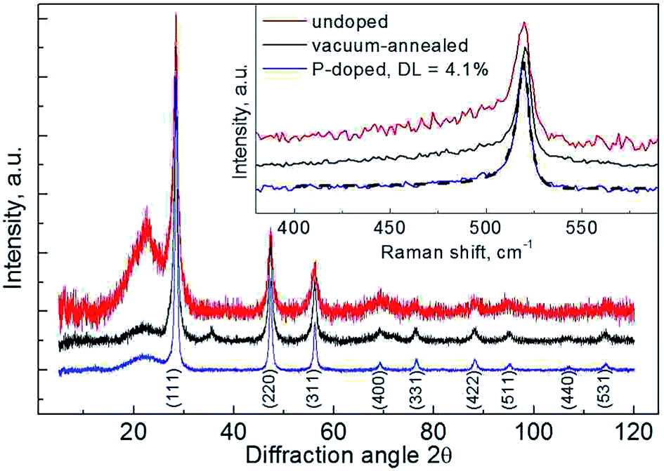 | ||
| Fig. 1 XRD patterns of samples: (red) – Si_0; (black) – Si_va; (blue) – Si_20. Inset – Raman spectra of the samples. Dashed line – result of approximation of Raman spectrum of the doped sample with asymmetric resonance curve (see eqn (1), main text). The curves are offset vertically for clarity. | ||
Results obtained from Raman spectroscopy confirm the presence of a-Si and its crystallization with annealing. Raman spectra of SNPs samples (Fig. 1, inset) distinctively illustrate Fano-type peak positioned at ∼520 cm−1, corresponding to longitudinal optical (LO) – transverse optical (TO) phonon mode of Si lattice, and a lower wavenumber shoulder, which is attributed to vibrations in a-Si. The spectra are fit well by two components: an asymmetric resonance peak and a sum of two broad Gaussian components separated by 6 cm−1. The latter is a simplistic variation of the use of Gaussian-smeared vibrational density-of-states for c-Si accounting for scattering in a-Si.38 The shoulder feature is only significant for unannealed Si SNPs, with the intensity ratio of ∼0.4:1 to c-Si phonon peak. Thus we can conclude that crystallization of a-Si in the nanoparticles occurs upon annealing regardless of the presence of phosphorus.
The asymmetric lineshape used in modeling of Raman spectra is given by:39
 | (1) |
This form of curve was originally derived for transitions involving mixed discrete and continual (or pseudo- continual) states40 and is often used to fit Raman spectra of doped Si.6,39
Asymmetric resonance is presumed to originate from interaction between Γ-point optical phonons and a continuum of free carrier states.6 However, at the nanoscale undoped Si also exhibits asymmetric broadening of Raman features 41. Thus, a minor asymmetry effect does not readily prove the existence of free carriers. The position of LO–TO phonon mode of Si in Raman spectra is dependent on the surface-to-volume ratio, and hence on the mean crystallite size.41 The size of SNPs was estimated to be ∼10 nm for all the samples with use of theoretical curve from ref. 42. This value differs significantly from the results of XRD analysis. That inconsistency, however, can be attributed to a number of parameters affecting the position of the phonon mode, including size distribution in ensemble,6,9,43 impurity incorporation44 and strain.45
Investigation of doped SNPs by TEM reveals agglomerates which obstruct accurate particle size determination. However, an analysis of the diffraction contrast and lattice projections allows estimation of mean diameter of SNPs to be in range of 15–30 nm (Fig. 2(a)). Corresponding ED pattern shows the presence of Si rings only, with no extra reflections provided by the impurities. This stands in agreement with XRD results. HRTEM images of individual SNPs (Fig. 2(b)) confirm their good crystallinity and structural perfection. Some of SNPs exhibit twinning structure, however the amount of such defects is much lower than reported for hyperdoped Si SNPs.10 EDX elemental mapping (Fig. 2(c)) clearly illustrates localization of oxygen on the external surface of Si agglomerates, which is consistent with the formation of native silicon oxide as a result of air exposure. The thickness of this layer was estimated to be around 2 nm. The distribution of phosphorus throughout the sample is homogeneous, with minor segregation appearing at the surface of SNPs. Thus, doping of Si/SiOx SNPs was achieved by annealing in phosphorus vapor. No significant sintering of the particles was observed by experimental methods mentioned above.
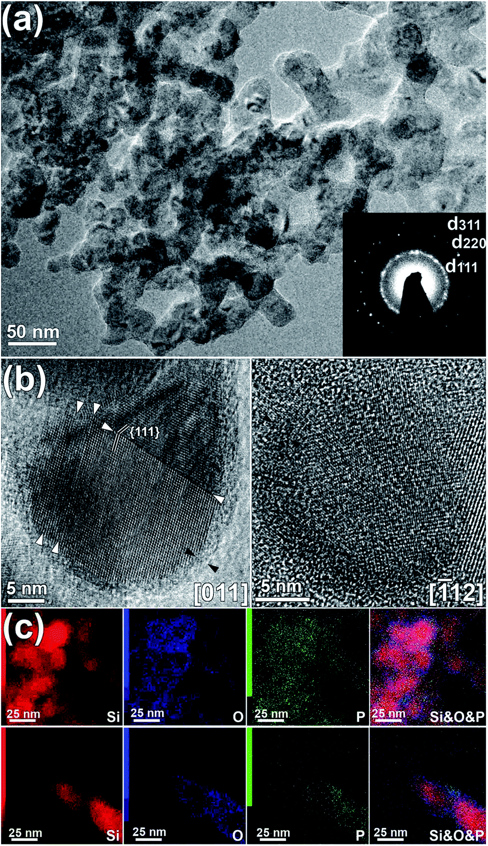 | ||
| Fig. 2 TEM study of P-doped sample Si_1.3: (a) low magnification bright field TEM image the inset ring ED pattern evidences Si structure. (b) bright field HRTEM images of single Si SNPs viewed along [011] and [−112] directions. Twin {111} planes are marked with white arrows. Si oxide layer is marked with black arrows. (c) EDX elemental mapping of Si K, O K, P K and overlaid color image (Si – red, O – blue, P – green). | ||
As doping of silicon is realized by diffusion, time, temperature and precursor vapor pressure appear to be the control parameters of the technique. In principle, complex vapor/temperature temporal profiles can be utilized to fabricate SNPs with specific concentration and distribution of an impurity.
In this study we have first considered the effect of precursor vapor pressure. Phosphorus content in doped SNPs as obtained by elemental analysis and quantitative EDX spectroscopy is represented in Table 1.
| Sample | NP/(NSi + NP) ratio% | As synthesized | After etching | ||||||
|---|---|---|---|---|---|---|---|---|---|
| Synthesis | ICP MS | LSPR position, cm−1 | Nc, cm−3 | Carrier activation efficiency | LSPR position, cm−1 | Nc, cm−3 | Carrier activation efficiency | ||
| Total | Core | ||||||||
| Si_0.6 | 0.6 | 0.126 | 0.19 | — | — | — | — | — | — |
| Si_1.3 | 1.3 | 0.28 | 0.15 | — | — | — | — | — | — |
| Si_2.5 | 2.5 | 0.44 | 0.29 | — | — | — | — | — | — |
| Si_9.1 | 9.1 | 2.5 | 1.1 | 1990 | 8.8 × 10¹⁹ | 7.0% | 2030 | 9.5 × 10¹⁹ | 17% |
| Si_20 | 20.0 | 4.1 | 0.95 | 1990 | 9.1 × 10¹⁹ | 4.5% | 2050 | 1.6 × 10²⁰ | 34% |
| Si_36 | 35.9 | 9.9 | 2.0 | 1840 | 4.0 × 10¹⁹ | 0.8% | 2050 | 1.3 × 10²⁰ | 13% |
The resulted values deviate significantly the initial composition in the reactor ampoule. Nevertheless, the specified and the obtained levels of impurity inclusion correlate well, indicating key role of precursor vapor pressure on the composition of SNPs (Fig. 3). Maximum doping level of 10% at was achieved by the method. Efficiency of dopant inclusion may likely be improved by tuning of annealing conditions.
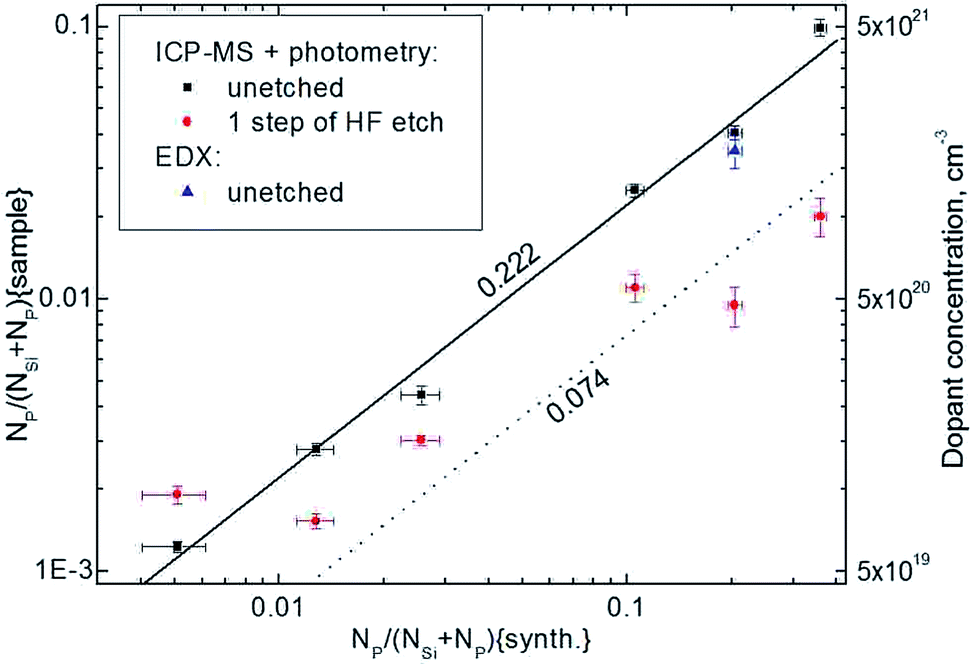 | ||
| Fig. 3 Results of elemental analysis of doped SNPs: ICP-MS and photometry analysis of unetched samples (■) and samples after 1 step of HF etching (●); EDX microanalysis of unetched samples (▲). The lines, representing constant levels of impurity inclusion in SNPs, are guides for the eye. | ||
As soon as some segregation of phosphorus was detected by EDX mapping, additional analysis was performed after HF etching of nanoparticles. Etching selectively removes SiOx layer of core/shell Si/SiOx nanoparticles, thus, phosphorus content in the etched samples should represent doping level in silicon core. Indeed, the quantitative analysis of silicon removal efficiency by single step etching was evaluated as ∼30%. On the other hand a dramatic decrease in phosphorus content was detected with etching (Table 1). Moreover, phosphorus loss correlates strongly with the initial phosphorus content and attains 85% for maximal doping levels. This illustrates that segregation of phosphorus appears to SiOx layer with the efficiency increasing strongly with the impurity content. Some kind of saturation is observed at ∼2% of phosphorus content in the etched samples, which can be assigned to the maximum P solubility in Si SNPs.
By the very definition every spatial position in a nanomaterial is at most in 50 nm proximity of a surface or interface. Thus significance of surface/interface states dramatically increases in SNPs comparing to bulk crystalline phases or disordered materials. Importantly, the hydrogenic impurities in Si can form stable complexes with dangling bonds, effectively negating the impact of both defects on the electronic structure of SNPs as it was predicted by ab initio calculations.25,45 This compensation has experimentally been observed as an offset of an impurity influence on the conductivity6 or Seebeck coefficient4 of laser-annealed films made of Si SNPs. The value of the offset of 1018 to 1019 cm−3 is consistent with the surface concentration of defects (1011 to 1012 cm−2)37 and surface-to-volume ratio of ∼6 × 106 cm−1 (for ∼10 nm Si nanoparticles). It is thus imperative to probe the electrical activity of the impurity in SNPs.
The pellets made of doped SNPs illustrate a serious rise in the conductivity of at least 2 orders of magnitude as compared to the undoped sample. Results of thermoelectric measurements are given in Section S.I of the ESI.† The thermopower had a positive sign, consistent with n-type doping of silicon. Absolute values of Seebeck coefficient were established as 590, 500, 130, 170 μV K−1 for Si_0.6, Si_1.3, Si_2.5 and Si_36 samples correspondingly. This generally inverse relation of Seebeck coefficient and impurity content can be explained in terms of Fermi level shift towards the conduction band and expected linear dependence of the Seebeck coefficient on the energy difference between Fermi level and the edge of the band.4,11
In the strongly doped samples the existence of free charge carriers was confirmed independently through the observation of LSPR mode in their IR spectra (Fig. 4). The spectra include vibrations corresponding to SiOx (1100 and 1200 cm−1), H2O and hydroxyl (3000–3700 cm−1), methyl (2960 cm−1) and methylene (2860, 2930 cm−1) group vibrations superimposed on a prominent LSPR band with a FWHM of ∼2000 cm−1. Details of designation of bands to group frequencies are given in Section S.II of the ESI.†
 | ||
| Fig. 4 IR spectra of Si SNPs samples: (black) – Si_0; (red) – Si_1.3; (blue) – Si_9.1; (cyan) – Si_20; (magenta) – Si_36. Dotted curves – approximations of the optical response (see main text). Inset – log plot of IR spectra of sample Si_20. Dashed line indicates the slope of linearized portion of the log plot. The curves are offset vertically for clarity. | ||
LSPR of nanoparticles is often described in terms of Mie absorption theory for microspheres in quasi-static limit:46,47
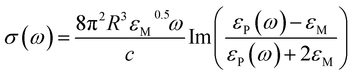 | (2) |
 | ||
| Fig. 5 The effect of degassing of plasmonic samples in argon on the form of IR spectrum: (black) – spectrum of etched sample Si_36 prior to degassing, (red) – spectrum of the same sample after degassing. Inset – the effect of temperature on the plasmonic band: changes in position of maximum of LSPR band (■) of sample Si_20 with temperature (●) in two heating/cooling cycles. | ||
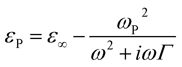
Dielectric function of plasmonic SNPs is frequently modeled assuming their degenerate state with use of Drude equation:
 | (3) |
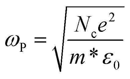
Free carrier concentration in SNPs is extracted from ωp value with following equation:9–11,49
 | (4) |
It is worth noting that inactive excess phosphorus at the interface may also trap charge carriers, as we observe lower η values for samples with higher impurity content. Possibility of acceptor behavior of phosphorus in oxide-embedded P-doped Si nanocrystals was demonstrated with X-ray absorption near edge structure spectroscopy.52
Plasmonic behavior of SNPs can provide even deeper insight into distribution of an impurity within the particles. As IR spectroscopy requires only a small amount of the material, studies of up to 4 steps of sequential etching were accomplished (Fig. 6). Observed variation in ωp can be well explained with carrier trapping. Existence of LSPR in SNPs is often connected to the surface/interface quality in terms of concentration of trap states.9,13 HF etching is known to efficiently reduce the surface concentration of Pb centers at Si/SiOx interface,37 which accounts for the increased Nc on the initial etching step. A gradual decrease of ωp with further etching steps is then ascribed to an increase of surface-to-volume ratio of the particles.
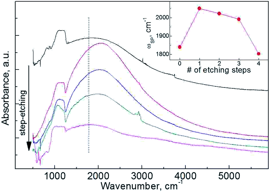 | ||
| Fig. 6 Evolution of LSPR absorption band of sample Si_36 during the step-etching process, as-synthesized sample and 4 steps of HF etch are shown. The spectra are offset vertically for clarity and normalized for areal intensity of SiOx group vibration features. Dashed vertical line denotes the original position of maximum of LSPR band and is a guide for the eye. Inset – the position of LSPR band maximum as a function of number of etching steps. | ||
As plasmonic response is present for all the etched samples we can conclude that phosphorus diffuses deep into the nanoparticles' cores. LSPR band evolution with step etching and HAADF-STEM elemental mapping are consistent with uniform radial distribution of phosphorus in silicon cores.
Thus the proposed diffusion doping technique provides valuable doping levels of SNPs with high generation efficiency to induce multiple in-particle carrier generation for LSPR response.
Doped SNPs with well-controlled size and impurity position distribution are desired for construction of devices. This is most evident when examining transport properties of SNPs. Monodisperse particles show enhanced conductivity in a nanocrystalline superlattice due to propagation of delocalized states.53 Contrarily, polydispersity leads to emergence of Anderson localization regime.1 Single impurities have been shown to give rise to backscattering in silicon nanowires, with variance in impurity position potentially leading to a drop of conduction in large energy window.45 Decomposition of silane, which is currently the most prominent method of synthesis of doped Si SNPs, naturally leads to polydisperse ensembles of particles. At the same time, post-synthetic diffusion doping may be easily coupled with techniques capable of producing monodisperse Si SNPs (e.g. decomposition of hydrogen silsesquioxane54), high-throughput techniques like plasma chemical synthesis from condensed phase,55 low-cost ball milling techniques.56,57
IV Conclusions
We have described a simple technique for diffusion doping of Si SNPs with phosphorus from a gaseous phase. Phosphorus vapor pressure was established as a main parameter for quantitative control of SNPs' DLs up to 10% at. According to EDX elemental mapping the method results in rather uniform distribution of phosphorus in the ensemble, providing equivalent doping of silicon SNPs. Highly doped nanoparticles exhibit well-pronounced thermoelectric and plasmonic properties proving implantation of P into nanocrystalline silicon cores. The particles are air-stable, providing no shift of plasmonic frequencies in time due to natural oxide shell. Fitting of LSPR allowed to determine free carrier concentrations exceeding 1020 cm−3 with dopant activation efficiencies up to 34%. Temperature dependence of LSPR and its lineshape also confirmed significance of electron–phonon interaction in plasmonic Si SNPs, which can become a potential bottleneck for shifting the LSPR band position towards the visible part of the spectrum.In conjunction with etching the technique can provide a great variety of P radial profiles in Si SNPs. This may prove useful in characterization of the influence of impurity position on the properties of nanoparticles, such as LSPR and thermopower, as well as in tuning thereof. The technique is potentially beneficial for n-type doping of SNPs with other group 15 elements (As, Sb) providing suitable precursors with high enough vapor pressure.
Conflicts of interest
There are no conflicts of interest to declare.Acknowledgements
This work was supported by Russian Foundation for Basic Research grant No 17-03-01269. The authors acknowledge (partial) support from M. V. Lomonosov Moscow State University Program of Development.References
- D. V. Talapin and C. B. Murray, Science, 2005, 310, 86 CrossRef PubMed.
- J. Jang, D. S. Dolzhnikov, W. Liu, S. Nam, M. Shim and D. V. Talapin, Nano Lett., 2015, 15, 6309 CrossRef PubMed.
- J. van Embden, A. S. R. Chesman, E. Della Gaspera, N. W. Duffy, S. E. Watkins and J. J. Jasieniak, J. Am. Chem. Soc., 2014, 136, 5237 CrossRef PubMed.
- R. Lechner, H. Wiggers, A. Ebbers, J. Steiger, M. S. Brandt and M. Stutzmann, Phys. Status Solidi RRL, 2007, 1, 262 CrossRef.
- I. Kriegel, J. Rodríguez-Fernández, A. Wisnet, H. Zhang, C. Waurisch, A. Eychmüller, A. Dubavik, A. O. Govorov and J. Feldmann, ACS Nano, 2013, 7, 4367 CrossRef PubMed.
- R. Lechner, A. R. Stegner, R. N. Pereira, R. Dietmueller, M. S. Brandt, A. Ebbers, M. Trocha, H. Wiggers and M. Stutzmann, J. Appl. Phys., 2008, 104, 053701 CrossRef.
- J. A. Faucheaux, A. L. D. Stanton and P. K. Jain, J. Phys. Chem. Lett., 2014, 5, 976 CrossRef PubMed.
- X. Pi and C. Delerue, Phys. Rev. Lett., 2013, 111, 177402 CrossRef PubMed.
- S. Zhou, X. Pi, Z. Ni, Y. Ding, Y. Jiang, C. Jin, C. Delerue, D. Yang and T. Nozaki, ACS Nano, 2015, 9, 378 CrossRef PubMed.
- D. J. Rowe, J. S. Jeong, K. A. Mkhoyan and U. R. Kortshagen, Nano Lett., 2013, 13, 1317 CrossRef PubMed.
- S. Zhou, Z. Ni, Y. Ding, M. Sugaya, X. Pi and T. Nozaki, ACS Photonics, 2016, 3, 415 CrossRef.
- S. Zhou, X. Pi, Z. Ni, Q. Luan, Y. Jiang, C. Jin, T. Nozaki and D. Yang, Part. Part. Syst. Charact., 2015, 32, 213 CrossRef.
- N. J. Kramer, K. S. Schramke and U. R. Kortshagen, Nano Lett., 2015, 15, 5597 CrossRef PubMed.
- M. R. Scriba, D. T. Britton and M. Härting, Thin Solid Films, 2011, 519, 4491 CrossRef.
- X. D. Pi, R. Gresback, R. W. Liptak, S. A. Campbell and U. Kortshagen, Appl. Phys. Lett., 2008, 92, 123102 CrossRef.
- A. Mimura, M. Fujii, S. Hayashi, D. Kovalev and F. Koch, Phys. Rev. B, 2000, 62, 12625 CrossRef.
- M. Perego, G. Seguini and M. Fanciulli, Surf. Interface Anal., 2013, 45, 386 CrossRef.
- H. Gnaser, S. Gutsch, M. Wahl, R. Schiller, M. Kopnarski, D. Hiller and M. Zacharias, J. Appl. Phys., 2014, 115, 034304 CrossRef.
- T. Makimura, Y. Yamamoto, S. Mitani, T. Mizuta, C. Q. Li, D. Takeuchi and K. Murakami, Appl. Surf. Sci., 2002, 197–198, 670 CrossRef.
- L. Tsybeskov, K. D. Hirschman, S. P. Duttagupta, M. Zacharias, P. M. Fauchet, J. P. McCaffrey and D. J. Lockwood, Appl. Phys. Lett., 1998, 72, 43 CrossRef.
- G.-R. Lin, C.-J. Lin and H.-C. Kuo, Appl. Phys. Lett., 2007, 91, 093122 CrossRef.
- I. Perez-Wurfl, X. Hao, A. Gentle, D.-H. Kim, G. Conibeer and M. A. Green, Appl. Phys. Lett., 2009, 95, 153506 CrossRef.
- G.-R. Lin, Y.-H. Pai, C.-T. Lin and C.-C. Chen, Appl. Phys. Lett., 2010, 96, 263514 CrossRef.
- N. P. Lyakishev, State diagrams of double metallic systems, Mashinostroyenie, Moscow, 2001 Search PubMed.
- Z. Ni, X. Pi and D. Yang, Phys. Rev. B, 2014, 89, 035312 CrossRef.
- A. Carvalho, S. Öberg, M. Barroso, M. J. Rayson and P. Briddon, Phys. Status Solidi A, 2012, 209, 1847 CrossRef.
- R. Guerra and S. Ossicini, J. Am. Chem. Soc., 2014, 136, 4404 CrossRef PubMed.
- M. Perego, G. Seguini, E. Arduca, J. Frascaroli, D. de Salvador, M. Mastromatteo, A. Carnera, G. Nicotra, M. Scuderi, C. Spinella, G. Impellizzeri, C. Lenardi and E. Napolitani, Nanoscale, 2015, 7, 14469 RSC.
- F. Ruffino, L. Romano, E. Carria, M. Miritello, M. G. Grimaldi, V. Privitera and F. Marabelli, J. Nanotechnol., 2012, 2012, 635705 Search PubMed.
- G. A. Kachurin, S. G. Yanovskaya, D. I. Tetelbaum and A. N. Mikhaylov, Phys. Tech. Semicond., 2003, 37, 738 Search PubMed.
- P. G. Kik, M. L. Brongersma and A. Polman, Appl. Phys. Lett., 2000, 76, 2325 CrossRef.
- N. N. Kononov, G. P. Kuz'min, A. N. Orlov, O. V. Tikhonevitch and A. A. Surkov, Phys. Tech. Semicond., 2005, 39, 868 Search PubMed.
- I. S. Grigor'ev and E. Z. Mejlihov, Physical values, Energoatomizdat, Moscow, 1991 Search PubMed.
- L. V. Myshlyaeva and V. V. Krasnoschokov, Analytical chemistry of silicon, Nauka, Moscow, 1972 Search PubMed.
- P. L. Buldini and D. Sandrini, Anal. Chim. Acta, 1978, 98, 401 CrossRef.
- V. Petricek, M. Dusek and L. Palatinus, Z. Kristallogr., 2014, 229(5), 345 Search PubMed.
- S. Niesar, A. R. Stegner, R. N. Pereira, M. Hoeb, H. Wiggers, M. S. Brandt and M. Stutzmann, Appl. Phys. Lett., 2010, 96, 193112 CrossRef.
- J. E. Smith Jr., M. H. Brodsky, B. L. Crowder and M. I. Nathan, Phys. Rev. Lett., 1971, 26, 642 CrossRef.
- N. H. Nickel, P. Lengsfeld and I. Sieber, Phys. Rev. B, 2000, 61, 15558 CrossRef.
- U. Fano, Phys. Rev., 1961, 124, 1866 CrossRef.
- K. H. Khoo, A. T. Zayak, H. Kwak and J. R. Chelikowsky, Phys. Rev. Lett., 2010, 105, 115504 CrossRef PubMed.
- H. Richter, Z. P. Wang and L. Ley, Solid State Commun., 1981, 39, 625 CrossRef.
- W. Kim and A. Majumdar, J. Appl. Phys., 2006, 99, 084306 CrossRef.
- K. H. Khoo and J. R. Chelikowsky, Phys. Rev. B, 2014, 89, 195309 CrossRef.
- M.-V. Fernández-Serra, C. Adessi and X. Blase, Nano Lett., 2006, 6, 2674 CrossRef PubMed.
- R. J. Mendelsberg, G. Garcia, H. Li, L. Manna and D. J. Milliron, J. Phys. Chem. C, 2012, 116, 12226 Search PubMed.
- C. F. Bohren and D. R. Huffman, Absorption and Scattering of Light by Small Particles; Wiley-VCH: Weinheim, 2004 Search PubMed.
- S. Link and M. A. El-Sayed, J. Phys. Chem. B, 1999, 103, 4212 CrossRef.
- J. Ederth, P. Johnsson, G. A. Niklasson, A. Hoel, A. Hultåker, P. Heszler, C. G. Granqvist, A. R. van Doorn, M. J. Jongerius and D. Burgard, Phys. Rev. B, 2003, 68, 155410 CrossRef.
- H. Zhang, R. Zhang, K. S. Schramke, N. M. Bedford, K. Hunter, U. R. Kortshagen and P. Nordlander, ACS Photonics, 2017, 4, 963 CrossRef.
- T.-L. Chan, M. L. Tiago, E. Kaxiras and J. R. Chelikowsky, Nano Lett., 2008, 8, 596 CrossRef PubMed.
- D. Konig, S. Gutsch, H. Gnaser, M. Wahl, M. Kopnarski, J. Gottlicher, R. Steininger, M. Zacharias and D. Hiller, Sci. Rep., 2015, 5, 9702 CrossRef PubMed.
- S. Xu, D. Thian, S. Wang, Y. Wang and F. B. Prinz, Phys. Rev. B, 2014, 90, 144202 CrossRef.
- M. Dasog, Z. Yang, S. Regli, T. M. Atkins, A. Faramus, M. P. Singh, E. Muthuswamy, S. M. Kauzlarich, R. D. Tilley and J. G. C. Veinot, ACS Nano, 2013, 7, 2676 CrossRef PubMed.
- I. A. Tutorskii, A. I. Belogorokhov, A. A. Ishchenko and P. A. Storozhenko, Colloid J., 2005, 67, 491 CrossRef.
- Y. Jin, S. Zhang, B. Zhu, Y. Tan, X. Hu, L. Zong and J. Zhu, Nano Lett., 2015, 15, 7742 CrossRef PubMed.
- L. Zong, Y. Lin, C. Liu, B. Zhu, X. Hu, Z. Lu and J. Zhu, Nano Lett., 2016, 16, 7210 CrossRef PubMed.
Footnote |
| † Electronic supplementary information (ESI) available. See DOI: 10.1039/c8ra03260b |
| This journal is © The Royal Society of Chemistry 2018 |