
 Open Access Article
 This Open Access Article is licensed under a Creative Commons Attribution-Non Commercial 3.0 Unported Licence
Highly stable ITO/Zn2TiO4/Pt resistive random access memory and its application in two-bit-per-cell
Shi-Xiang Chen,
Sheng-Po Chang *,
Wei-Kang Hsieh,
Shoou-Jinn Chang and
Chih-Chien Lin
*,
Wei-Kang Hsieh,
Shoou-Jinn Chang and
Chih-Chien Lin
Institute of Microelectronics and Department of Electrical Engineering, Advanced Optoelectronic Technology Center, National Cheng Kung University, Tainan 70101, Taiwan. E-mail: changsp@mail.ncku.edu.tw
First published on 15th May 2018
Abstract
We discuss the fabrication procedure and device characteristics of ITO/Zn2TiO4/Pt resistive random-access memory (RRAM) at room temperature. Four different resistive states were obtained by applying different current compliances, all of which showed good retention characteristics with no obvious degradation and were individually distinguished after 10![[thin space (1/6-em)]](https://www.rsc.org/images/entities/char_2009.gif) 000 s at a read voltage of 100 mV. The multilevel memory effect can be attributed to the combination of the radial growth of filaments and the formation of conductive filaments when applying different compliance current values during the set process. The set and reset voltages of the ITO/Zn2TiO4/Pt RRAM device were maintained within ±1 V. The device performed well at low operation voltages. The mechanisms of multilevel resistive switching characteristics were investigated to illustrate the multilevel carrier conduction phenomenon associated with Zn2TiO4-based RRAM devices. In this study, our group illustrated the application of zinc titanate (Zn2TiO4) in non-volatile memories for the first time.
000 s at a read voltage of 100 mV. The multilevel memory effect can be attributed to the combination of the radial growth of filaments and the formation of conductive filaments when applying different compliance current values during the set process. The set and reset voltages of the ITO/Zn2TiO4/Pt RRAM device were maintained within ±1 V. The device performed well at low operation voltages. The mechanisms of multilevel resistive switching characteristics were investigated to illustrate the multilevel carrier conduction phenomenon associated with Zn2TiO4-based RRAM devices. In this study, our group illustrated the application of zinc titanate (Zn2TiO4) in non-volatile memories for the first time.
Introduction
In the past few decades, the applications of non-volatile memories (NVMs) in consumer electronics have become ubiquitous.1 However, with the development of integrated circuit fabrication technologies and semiconductor device die shrinks, floating gate memories became gradually devalued.2 In response, some types of NVMs have been investigated.3–13 Accordingly, resistive random-access memory (RRAM) devices have attracted great attention. RRAM exhibit advantageous properties such as simple structure, low power consumption, high switching speed, and high integrating density. Owing to its uncomplicated formation, the RRAM device has been widely evaluated for its compatibility with common complementary metal-oxide-semiconductor (CMOS) devices.14–17 By virtue of these excellent properties, RRAM has great potential for application in next-generation NVMs.For RRAM devices, several materials such as ZrN,18 SiN,19 ZnO,20 MgO,21,22 Al2O3,23,24 AlN,25,26 Ni27,28, and TiO2,29,30 have been widely investigated. Among these devices, the TiO2-based RRAM device has gained interest for its high ratio between the high resistance state (HRS) and the low resistance state (LRS). The resistive switching (RS) mechanism of RRAM is influenced by the formation and rupture of conduction filaments within the active layer due to the thermal Hall effect between the top (TE) and bottom electrodes (BE). The conduction paths depend on the oxygen vacancies and ion movements inside the oxide layers. The filament model of oxygen vacancy/ion migration was used to explain the RRAM RS behaviour observed during the program/erase procedure. Previous studies reported the RS characteristics of transition metal oxide-based RRAM devices, which were confirmed by the distribution of localized oxygen vacancies in the oxide layer.
ZnO–TiO2 alloy systems, such as ZnTiO3, Zn2TiO4, and Zn2Ti3O8, exhibited great potential as phosphors, catalysts, microwave devices, low-temperature co-fired ceramics (LTCCs), and dielectrics.31–34 Moreover, zinc titanate (Zn2TiO4), with an inverse spinel structure, has been used as a catalyst and dielectric in manufacturing. Its physical features, optical properties, and electrical characteristics have been studied for dielectric applications.35,36 Herein, a Zn2TiO4 RRAM device with an ITO/Zn2TiO4/Pt metal-insulator-metal (MIM) structure was fabricated and investigated. The RS behaviour of this RRAM device was systematically studied based on the forming and operation voltages, operation currents, high/low resistance ratio using methods such as RS cycle and retention time tests. The electrical properties and fabrication methods of the device were also discussed comprehensively.
Experiment
The MIM structure of the ITO/Zn2TiO4/Pt RRAM device adopted in this study is shown in Fig. 1. The glass substrate was treated with acetone, isopropyl alcohol, and deionized (DI) water by ultrasonic concussion before the fabrication process. Initially, a Ti layer of around 100 nm was grown on the substrate as an adhesion layer using an electron gun (e-gun) thermal evaporation system. Subsequently, a Pt layer of around 300 nm was deposited onto the Ti metal layer as the BE. Furthermore, a 70 nm Zn2TiO4 thin film active layer was grown using a radio frequency (RF) magnetron sputter system with a 99.99% Zn2TiO4 target under 10 mtorr and mixed argon and oxygen gas flow (30 and 10 sccm, respectively) at room temperature and 80 W RF power. The Zn2TiO4 active layer surface was 1500 × 1500 μm2. Finally, a 50 nm thick ITO layer was fabricated as the TE by RF magnetron sputtering at room temperature, with a 99.99% ITO target (SnO2: 10 wt%), process power of 50 W, Ar flow of 99 sccm, O2 flow of 0.7 sccm, and chamber pressure of 3 mtorr. The ITO top electrode had dimensions 500 × 500 μm2.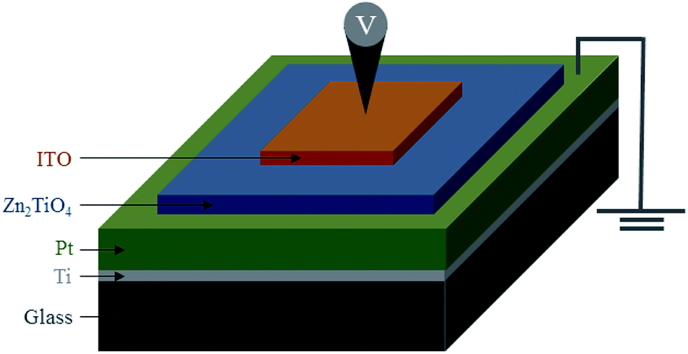 | ||
| Fig. 1 Schematic diagram of the ITO/Zn2TiO4/Pt RRAM device. | ||
The crystalline characteristics of the Zn2TiO4 thin film were measured using a multipurpose X-ray thin film diffractometer (XRD, Rigaku D/MAX2500) at the Instrument Center of National Cheng Kung University (NCKU). The composition and thickness of the ITO/Zn2TiO4/Pt RRAM device were measured by transmission electron microscopy (TEM, JEM-2010 Electron Microscope) at the Center for Micro/Nano Science and Technology (CMNST), Tainan, Taiwan. The RS behaviour of the RRAM device was investigated by current–voltage (I–V) curve measurements at room temperature using a semiconductor parameter analyser (Agilent B1500) in the voltage scanning mode. Moreover, during the I–V measurements, a bias voltage was applied onto the ITO TE, while the Pt BE was grounded electrically.
Results and discussion
To distinguish each layer, TEM cross-sectional analysis was performed, as shown in Fig. 2. Notably, the TEM image of the ITO/Zn2TiO4/Pt structure revealed four layers, namely, Ti adhesion layer, Pt bottom electrode, Zn2TiO4 active layer, and ITO top electrode, on the glass substrate. The measured thickness of the Zn2TiO4 film was approximately 70 nm.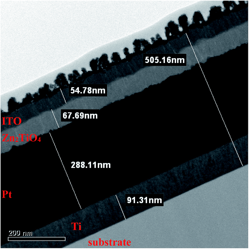 | ||
| Fig. 2 Cross-sectional HRTEM image of the ITO/Zn2TiO4/Pt RRAM device. | ||
To analyse the crystal structure of the fabricated thin film layer, XRD was performed. The resultant spectrum is shown in Fig. 3. Only a small peak of SiO2 (100) was observed, suggesting that the Zn2TiO4 active layer might be amorphous. To confirm this, TEM bright-field observations and electron diffraction analysis were performed. In this case, the TEM bright-field image of the fabricated Zn2TiO4 thin film active layer and its corresponding electron diffraction patterns were presented in Fig. 4(a) and (b), thus allowing us to clarify its crystalline characteristics.
 | ||
| Fig. 3 XRD spectrum of the Zn2TiO4 thin film grown on a glass substrate. | ||
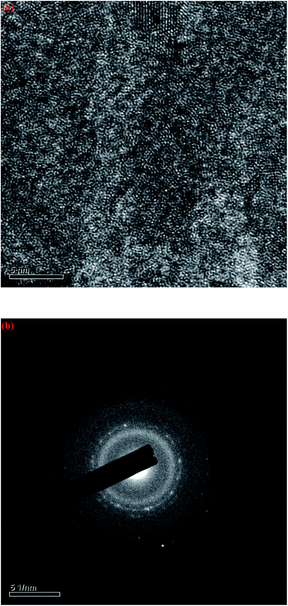 | ||
| Fig. 4 (a) TEM bright-field image of ITO/Zn2TiO4/Pt structure and (b) its corresponding electron diffraction pattern. | ||
Based on the cross-sectional image shown in Fig. 4(a), Zn2TiO4 retained its crystal orientation in the fabricated RRAM device. Fig. 4(b) shows the HRTEM electron diffraction pattern, indicating that the Zn2TiO4 layer is polycrystalline, with very weak signals corresponding to four crystal orientations. The d-spacing values of these crystals are 0.2275, 0.1412, 0.1199, and 0.1194 nm, corresponding to the crystal orientations (212), (330), (430), and (414) of the tetragonal structure, respectively.37,38 Here, the low crystallinity of the Zn2TiO4 layer resulted in a feeble signal in the XRD plot shown in Fig. 3. Hence, further effort is required to accurately analyse its features.
Fig. 5 demonstrates the first positive voltage sweep of the Zn2TiO4 RRAM device, which shows that the measured current hardly increased initially, and then suddenly rose at around 25 V, the voltage for the electro-forming process. This dramatic change indicated that the RRAM device switched from HRS to LRS. This reversible RS behaviour was observed after the forming process, with a compliance current (CC) value of 0.01 mA to protect the device from hard breakdown. Fig. 6 shows the bipolar resistance switching behaviour of the fabricated Zn2TiO4 RRAM under direct current (DC) voltage sweeping operations after the forming process with different compliance currents. During the set process, a current compliance of 1 mA was applied to protect the device. In Fig. 6(a), the RRAM device switched from the HRS to the LRS at a set voltage of around 0.6 V. This transferred the oxygen-vacancies from BE to TE. As the voltage varied, oxygen-vacancies arranged themselves to form a continuous conductive filament between the TE and BE. Furthermore, the RRAM device reverted from the LRS to the HRS at an adequate reset voltage of around −0.6 V and a CC of 5 mA. The set/reset process was performed over 500 times to verify the resistance switching reliability of the RRAM device. The result shown in Fig. 6(b) was obtained under set and reset CC values of 10 and 20 mA, respectively. Similar bipolar RS behaviours were observed in Fig. 6(a) and (b). In both, each cycle of the set RS from HRS has its unique current value. This is because the rupture of conductive filament in the reset process results in different oxygen-vacancy migrations toward the BE when the device enters the HRS. Hence, different resistances of the RRAM device are produced. The multilevel operation of the ITO/Zn2TiO4/Pt RRAM device was confirmed by employing different CC values, as shown in Fig. 6(a) and (b).
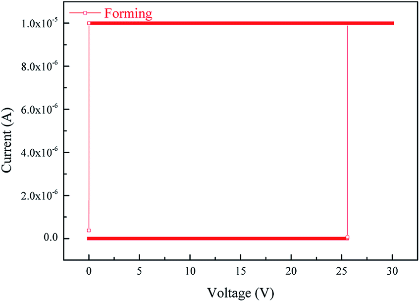 | ||
| Fig. 5 I–V curves of ITO/Zn2TiO4/Pt RRAM device in forming process. | ||
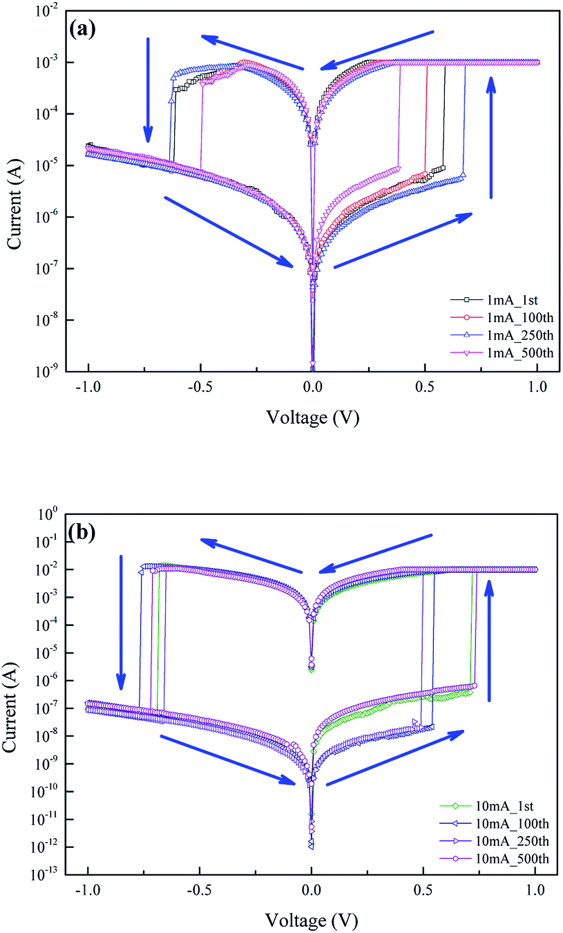 | ||
| Fig. 6 Resistance switching characteristics of the ITO/Zn2TiO4/Pt RRAM device with a compliance current of (a) 1 mA; (b) 10 mA. | ||
Fig. 7(a), which is the integration of the previous two RS plots, displays four distinct resistance states at 100 mV. These are labelled as 00, 01, 10, and 11, corresponding to the highest resistance state (HHS), high resistance state (HRS), low resistance state (LRS), and lowest resistance state (LLS), respectively. Moreover, the asymmetric RS characteristics in the HHRS with 10 mA CC were attributed to the resistance distributions caused by the rupture of the conductive filament during a reset process with high CC.
 | ||
| Fig. 7 The resistance switching characteristics of the ITO/Zn2TiO4/Pt RRAM (a) evaluated by applied different compliance current value; (b) measured at 100 mV for over 500 cycles; (c) cumulative probabilities. | ||
Fig. 7(b) represents the RS behaviour of the fabricated RRAM device. For over 500 cycles, four resistance states were measured at 100 mV. The ratios of the order of current magnitudes are around 0.5, 2, and 0.5 between HHS and HRS, HRS and LRS, and LRS and LLS, respectively. This aids in determining the different bit storage abilities of the memory cells. The RS characteristics of the four states could be distinguished after 500 cycles. Therefore, the HHS/HRS/LRS/LLS distribution data in Fig. 7(c) could provide further information about the resistance variation between each state on the same memory cell of the RRAM device. The calculated cumulative probabilities of the resistance in each state suggest that the states do not interfere with each other. Thus, the probability for data storage failure is very slim. Fig. 8(a) displays the retention characteristics and resistance variations of HHS, HRS, LRS, and LLS at a constant operating voltage of 100 mV. For the retention time test, no significant variation was observed in all the states. Moreover, the ratios of the order of current magnitudes are 0.5, 2 and 3 between HHS and HRS, HRS and LRS, and LRS and LLS, respectively. Additionally, the retention distribution information for these states is shown in Fig. 8(b), where minimal variation was observed. With RS and retention properties, our ITO/Zn2TiO4/Pt RRAM device is capable of multilevel data storage.
 | ||
| Fig. 8 The retention characteristics of the ITO/Zn2TiO4/Pt RRAM (a) measured at 100 mV; (b) cumulative probabilities. | ||
The RS performance of the RRAM device fabricated in this work was examined over 500 program/erase switching cycles. For the ITO/Zn2TiO4/Pt memory element, the result of the statistical analysis of the set and reset voltages for different current compliance values is shown in Fig. 9. The distributions of set voltage in 1 and 10 mA were comparable. However, the distributions of reset voltage were slightly different, causing different conduction filament formations and ruptures. With a reset procedure in RRAM device, could make a breaking of the conduction paths and a thin film layer consisted of Zn2TiO4 with higher quality (lower oxygen vacancies) were formed near Zn2TiO4/ITO interface where the conduction filaments were. By a higher reset current resulted from higher CC value could led to a thicker Zn2TiO4 film formed near the interface. And with such a grown Zn2TiO4 layer could result in a higher resistive state of the RRAM devices.
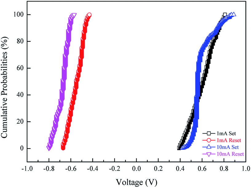 | ||
| Fig. 9 Set and reset voltage cumulative probability distributions of ITO/Zn2TiO4/Pt RRAM device with different compliance current values. | ||
To demonstrate the RS mechanisms in the HRS and HHS and determine the current transport in the memory cells, I–V curves were replotted and fitted, respectively. Fig. 10(a) shows the region of the I–V curve where the device switched from HRS to LRS. The results for 1 and 10 mA current compliance values are shown in Fig. 10(b) and (c), respectively. Therefore, we replotted the I–V curves on a double-logarithmic scale to illustrate the current transport mechanism in the fabricated RRAM cell. At 1 mA current compliance, the current conduction mechanism involved in the HRS was prompted by ohmic conduction, as evidenced by the linearity of the I–V curve with a slope of around 1. The RRAM device exhibited ohmic conduction after switching to the LRS. At 10 mA current compliance, the conduction mechanism involved in the HHS is initially governed by ohmic conduction with a slope of around 1. As the operation voltage increased, electrons transferred from the BE to the TE, and the slope increased to 2. This suggests that the conduction mechanism in HHS at higher bias voltages might be attributed to the space-charge-limited current (SCLC).39,40 Furthermore, the conduction mechanism reverted to ohmic conduction as the device switched to the LLS. Therefore, by this double-logarithmic scale analysis, the carrier conduction mechanisms of the ITO/Zn2TiO4/Pt RRAM device were observed.
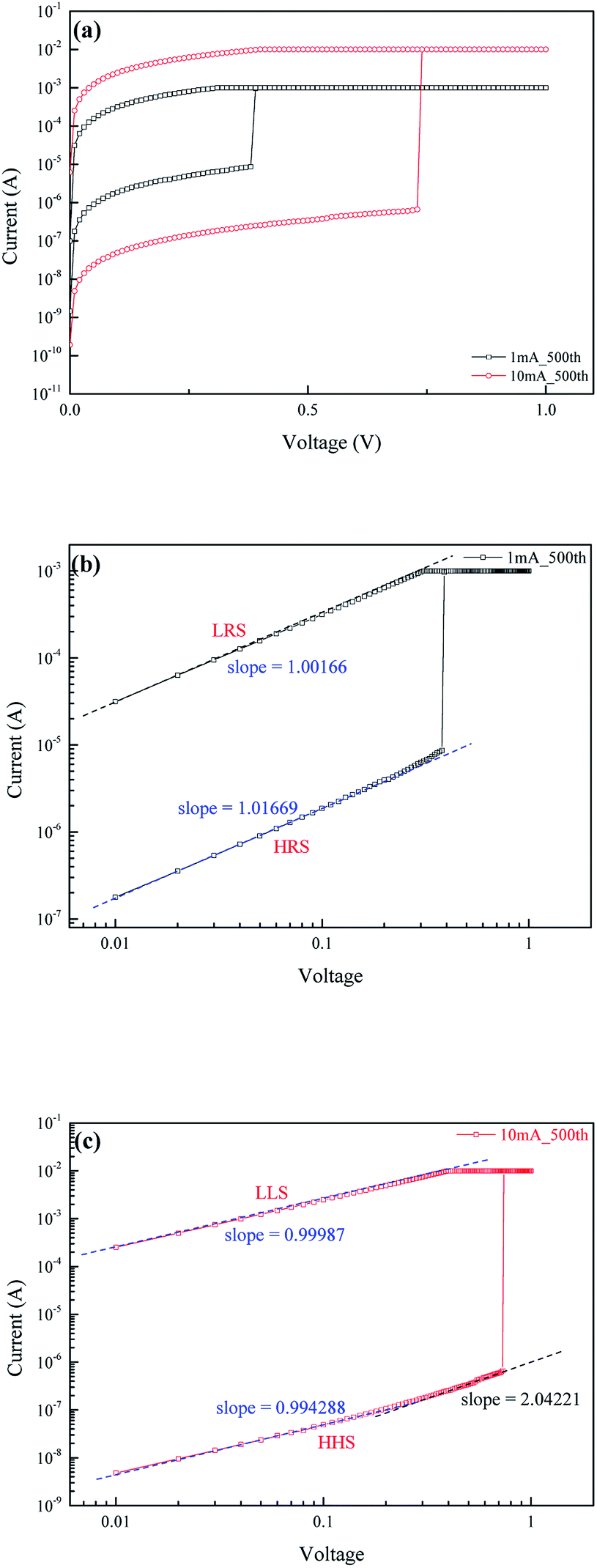 | ||
| Fig. 10 (a) Selected I–V region for the curve-fitting analysis of carrier transport at different compliance current values. The double-logarithmic scales correspond to (b) 1 mA and (c) 10 mA. | ||
Finally, to verify the retention stabilities of the RRAM device, we re-examined its performance after 1 month since our last measurement. As shown in Fig. 11(a), the retention characteristics of HHS, HRS, LRS, and LLS at the continuous read voltage of 100 mV were distinct. Furthermore, the ratios of the order of current magnitudes are around 0.5, 2, and 3 for HHS and HRS, HRS and LRS, and LRS and LLS, respectively. As shown in Fig. 11(b), the comparison between the retention characteristics of the original state and that of its counterpart after 1 month revealed no significant difference. Hence, we are quite confident that the data storage abilities of the RRAM device fabricated in this work did not experience any significant degradation. Furthermore, the device is stable and feasible in two-bit-per-cell applications with good reliability.
 | ||
| Fig. 11 The retention characteristics of the ITO/Zn2TiO4/Pt RRAM device (a) 1 month after the last measurement; and (b) the plot comparison between this and the original data. | ||
Conclusions
In this study, RRAM device with ITO/Zn2TiO4/Pt MIM structure was successfully proposed and fabricated at room temperature. Its I–V RS abilities displayed set/reset voltages within ±1 V, which is remarkable in low operating voltage applications. Furthermore, the superior bipolar RS performance persisted even after 500 successful switching cycles. Moreover, the product showed a strong retention performance for all four multilevel resistive states, which indicates its viability for two-bit-per-cell data storage applications. From the I–V measurement analysis, we found that the carrier conduction mechanism of the HRS is dominated by ohmic conduction at lower bias voltages and SCLC at higher bias voltages. The simply constructed ITO/Zn2TiO4/Pt RRAM device with four multilevel resistive states provided a useful alternative to the mass storage applications of non-volatile memory cells.Conflicts of interest
There are no conflicts to declare.Acknowledgements
This work was supported by the Ministry of Science and Technology [contract numbers MOST 106-2221-E-006-178 and MOST 105-2221-E-006-118]; the Center for Frontier Materials and Micro/Nano Science and Technology, National Cheng Kung University, Taiwan; and the Advanced Optoelectronic Technology Center, National Cheng Kung University, for projects from the Ministry of Education.References
- Y. Li, S. Long, Q. Liu, Q. Wang, M. Zhang, H. Lv, L. Shao, Y. Wang, S. Zhang, Q. Zuo, S. Liu and M. Liu, Nonvolatile multilevel memory effect in Cu/WO3/Pt device structures, Phys. Status Solidi RRL, 2010, 4, 124–126 CrossRef.
- W. R. Chen, T. C. Chang, P.-T. Liu, P. S. Lin, C. H. Tu and C. Y. Chang, Formation of stacked Ni silicide nanocrystals for nonvolatile memory application, Appl. Phys. Lett., 2007, 90, 112108 CrossRef.
- K. W. Lee, B. G. Jeon, B. J. Min, S. G. Oh, H.-J. Lee, W. T. Lim, S. H. Cho, H. S. Jeong, C. H. Chung and K. N. Kim, Development of Embedded Non-Volatile FRAMs for High Performance Smart Cards, Journal of Semiconductor Technology and Science, 2004, 4, 251–257 Search PubMed.
- M. Miyake, J. Scott, X. Lou, F. Morrison, T. Nonaka, S. Motoyama, T. Tatsuta and O. Tsuji, Submicron three-dimensional trenched electrodes and capacitors for DRAMs and FRAMs: fabrication and electrical testing, J. Appl. Phys., 2008, 104, 064112 CrossRef.
- P. H. Bolivar, F. Merget, D. Kim, B. Hadam, and H. Kurz, Lateral design for phase change random access memory cells with low-current consumption, Institute of Semiconductor Electronics, RWTH Aachen University, Sommerfeldstr, 2004, vol. 24, p. 52056 Search PubMed.
- D. Krebs, S. Raoux, C. T. Rettner, G. W. Burr, M. Salinga and M. Wuttig, Threshold field of phase change memory materials measured using phase change bridge devices, Appl. Phys. Lett., 2009, 95, 082101 CrossRef.
- I. Prejbeanu, M. Kerekes, R. Sousa, H. Sibuet, O. Redon, B. Dieny and J. Nozières, Thermally assisted MRAM, J. Phys.: Condens. Matter, 2007, 19, 165218 CrossRef.
- N. Sakimura, T. Sugibayashi, T. Honda, H. Honjo, S. Saito, T. Suzuki, N. Ishiwata and S. Tahara, MRAM cell technology for over 500 MHz SoC, IEEE J. Solid-State Circuits, 2007, 42, 830–838 CrossRef.
- W. K. Hsieh and S. J. Chang, Bipolar Resistive Switching Characteristics of TaO2 RRAM, Sci. Adv. Mater., 2016, 8, 1108–1111 CrossRef.
- W. K. Hsieh, K. T. Lam and S. J. Chang, Asymmetric resistive switching characteristics of In2O3: SiO2 cosputtered thin film memories, J. Vac. Sci. Technol., B: Nanotechnol. Microelectron.: Mater., Process., Meas., Phenom., 2014, 32, 020603 Search PubMed.
- M. Zangeneh and A. Joshi, Design and optimization of nonvolatile multibit 1T1R resistive RAM, IEEE Transactions on Very Large Scale Integration (VLSI) Systems, 2014, 22, 1815–1828 CrossRef.
- T. C. Chang, F. Y. Jian, S. C. Chen and Y. T. Tsai, Developments in nanocrystal memory, Mater. Today, 2011, 14, 608–615 CrossRef.
- W. K. Hsieh, R. W. Chuang and S. J. Chang, Two-bit-per-cell resistive switching memory device with a Ti/MgZnO/Pt structure, RSC Adv., 2015, 5, 88166–88170 RSC.
- J. J. Huang, Y. M. Tseng, W. C. Luo, C. W. Hsu and T. H. Hou, One selector-one resistor (1S1R) crossbar array for high-density flexible memory applications, IEEE Int. Electron Devices Meet., 2011, 31.7.1–31.7.4 Search PubMed.
- J. Zhang, Y. Ding, X. Xue, Y. Wu, Y. Xie, and Y. Lin, A 3D RRAM using stackable 1TXR memory cell for high density application, In Communications, Circuits and Systems, 2009 International Conference, 2009, pp. 917–920 Search PubMed.
- M. Y. Hsu, Y. H. Shih, Y. D. Chih, C. J. Lin and Y. C. King, Gate contact resistive random access memory in nano scaled FinFET logic technologies, Jpn. J. Appl. Phys., 2017, 56, 04CE05 CrossRef.
- R. Aluguri and T. Y. Tseng, Overview of selector devices for 3-D stackable cross point RRAM arrays, IEEE J. Electron Devices Soc., 2016, 4, 294–306 CrossRef.
- H. D. Kim, M. J. Yun, K. H. Kim and S. Kim, Oxygen-doped zirconium nitride based transparent resistive random access memory devices fabricated by radio frequency sputtering method, J. Alloys Compd., 2016, 675, 183–186 CrossRef.
- H. D. Kim, M. J. Yun and S. Kim, Resistive switching characteristics of Al/Si3N4/p-Si MIS-based resistive switching memory devices, J. Korean Phys. Soc., 2016, 69, 435–438 CrossRef.
- G. Chen, C. Song, C. Chen, S. Gao, F. Zeng and F. Pan, Resistive Switching and Magnetic Modulation in Cobalt-Doped ZnO, Adv. Mater., 2012, 24, 3515–3520 CrossRef PubMed.
- F. C. Chiu, W. C. Shih and J. J. Feng, Conduction mechanism of resistive switching films in MgO memory devices, J. Appl. Phys., 2012, 111, 094104 CrossRef.
- H. H. Huang, W. C. Shih and C. H. Lai, Nonpolar resistive switching in the Pt/MgO/Pt nonvolatile memory device, Appl. Phys. Lett., 2010, 96, 193505 CrossRef.
- Y. Wu, B. Lee and H. S. P. Wong, Al2O3-Based RRAM Using Atomic Layer Deposition (ALD) With 1-μA RESET Current, IEEE Electron Device Lett., 2010, 31, 1449–1451 CrossRef.
- Y. Wu, S. Yu, B. Lee and P. Wong, Low-power TiN/Al2O3/Pt resistive switching device with sub-20 μA switching current and gradual resistance modulation, J. Appl. Phys., 2011, 110, 094104 CrossRef.
- C. Chen, Y. C. Yang, F. Zeng and F. Pan, Bipolar resistive switching in Cu/AlN/Pt nonvolatile memory device, Appl. Phys. Lett., 2010, 97, 083502 CrossRef.
- C. Chen, S. Gao, G. Tang, H. Fu, G. Wang, C. Song and F. Pan, Effect of electrode materials on AlN-based bipolar and complementary resistive switching, ACS Appl. Mater. Interfaces, 2013, 5, 1793–1799 Search PubMed.
- J. Y. Son, Y. H. Shin, H. Kim and H. M. Jang, NiO resistive random access memory nanocapacitor array on graphene, ACS Nano, 2010, 4, 2655–2658 CrossRef PubMed.
- U. Russo, D. Ielmini, C. Cagli and A. L. Lacaita, Filament conduction and reset mechanism in NiO-based resistive-switching memory (RRAM) devices, IEEE Trans. Electron Devices, 2009, 56, 186–192 CrossRef.
- H. Y. Jeong, Y. I. Kim, J. Y. Lee and S. Y. Choi, A low-temperature-grown TiO2-based device for the flexible stacked RRAM application, Nanotechnology, 2010, 21, 115203 CrossRef PubMed.
- C. Kugeler, C. Nauenheim, M. Meier, A. Rudiger, and R. Waser, Fast resistance switching of TiO2 and MSQ thin films for non-volatile memory applications (RRAM), In Non-Volatile Memory Technology Symposium 2008. 9th Annual, 2008, pp. 1–6 Search PubMed.
- H. T. Kim, S. Nahm, J. D. Byun and Y. Kim, Low-Fired (Zn, Mg)TiO3 Microwave Dielectrics, J. Am. Ceram. Soc., 1999, 82, 3476–3480 CrossRef.
- H. T. Kim, Y. Kim, M. Valant and D. Suvorov, Titanium incorporation in Zn2TiO4 spinel ceramics, J. Am. Ceram. Soc., 2001, 84, 1081–1086 CrossRef.
- S. K. Manik and S. K. Pradhan, Preparation of nanocrystalline microwave dielectric Zn2TiO4 and ZnTiO3 mixture and X-ray microstructure characterization by Rietveld method, Phys. E, 2006, 33, 69–76 CrossRef.
- Y. Qu, W. Zhou, Z. Ren, G. Wang, B. Jiang and H. Fu, Facile synthesis of porous Zn2Ti3O8 nanorods for photocatalytic overall water splitting, ChemCatChem, 2014, 6, 2258–2262 CrossRef.
- Z. Wang, S. K. Saxena and C. S. Zha, In situ X-ray diffraction and Raman spectroscopy of pressure-induced phase transformation in spinel Zn2TiO4, Phys. Rev. B, 2002, 66, 024103 CrossRef.
- A. C. Chaves, S. J. Lima, R. C. Araújo, M. A. M. Maurera, E. Longo, P. S. Pizani and I. M. G. dos Santos, Photoluminescence in disordered Zn2TiO4, J. Solid State Chem., 2006, 179, 985–992 CrossRef.
- Calculated from ICSD using POWD-12++ (1997).
- R. L. Millard, R. C. Peterson and B. K. Hunter, Study of the cubic to tetragonal transition in Mg2TiO4 and Zn2TiO4 spinels by 17O MAS NMR and Rietveld refinement of X-ray diffraction data, Am. Mineral., 1995, 80, 885–896 Search PubMed.
- K. Park and J. S. Lee, Reliable resistive switching memory based on oxygen-vacancy-controlled bilayer structures, RSC Adv., 2016, 6, 21736–21741 RSC.
- J. Park, H. Jeon, H. Kim, W. Jang, H. Song, H. Kim and H. Jeon, Stabilization of Ni conductive filaments using NH3 plasma treatment for electrochemical metallization memory, RSC Adv., 2015, 5, 68900–68905 RSC.
| This journal is © The Royal Society of Chemistry 2018 |