
 Open Access Article
 This Open Access Article is licensed under a Creative Commons Attribution-Non Commercial 3.0 Unported Licence
Ultraflexible, stretchable and fast-switching electrochromic devices with enhanced cycling stability†
Qian Liu‡
a,
Zijie Xu‡a,
Wu Qiua,
Chen Houa,
Yanan Wanga,
Peijian Yaoa,
Rui Yua,
Wenxi Guo *a and
Xiang Yang Liu*ab
*a and
Xiang Yang Liu*ab
aResearch Institute for Biomimetics and Soft Matter, College of Materials, College of Physical Science and Technology, Xiamen University, Xiamen, 361005, China. E-mail: wxguo@xmu.edu.cn
bDepartment of Physics, Faculty of Science, National University of Singapore, Singapore, 117542, Singapore. E-mail: phyliuxy@nus.edu.sg
First published on 23rd May 2018
Abstract
Ultraflexible electronics have received extensive attention due to their favorable properties, such as superior mechanical robustness, light weight and good compatibility with large-area roll-to-roll fabrication. Here we present a flexible sandwiched tungsten trioxide/silver nanotrough network/poly(3,4-ethylenedioxythiophene)–poly(styrene sulfonate) multi-layer transparent conducting electrode with prominent conductivity (sheet resistance as low as 1.08 Ω sq−1) and transparency (85%). In particular, the flexible transparent electrode exhibits excellent mechanical robustness upon bending and stretching. This hybrid electrode can be further adhered tightly to a layer of WO3 to form an electrochromic device, which simultaneously displays a rapid switching time (0.75 s/1.82 s for bleaching/coloring) and high cyclic performance (86% retention of the initial optical contrast after cycling for 30![[thin space (1/6-em)]](https://www.rsc.org/images/entities/char_2009.gif) 000 s). In addition, our electrode can also be fabricated on various flexible substrates, such as polyethylene cling wrap, polydimethylsiloxane and Ecoflex, with sustained electrochromic properties after bending, twisting, stretching and even strong kneading. Our work provides new opportunities for the next generation of flexible and wearable electronics applied on various flexible substrates.
000 s). In addition, our electrode can also be fabricated on various flexible substrates, such as polyethylene cling wrap, polydimethylsiloxane and Ecoflex, with sustained electrochromic properties after bending, twisting, stretching and even strong kneading. Our work provides new opportunities for the next generation of flexible and wearable electronics applied on various flexible substrates.
Introduction
With the development of smart and portable electronic devices, gradually more and more electronic devices, such as sensors, displays and batteries, are required to be lightweight, deformable and even wearable.1–4 Electrochromic devices (ECDs), which can control the transmission of sunlight by varying its color, can realize energy savings of up to 50% when utilized as smart windows.5 The next generation of ideal flexible ECDs (i.e. flexible electrochromic (EC) displays and smart clothes) should maintain high mechanical performance without degradation, even upon bending, twisting or stretching,6,7 which is rather difficult to accomplish for conventional rigid ECDs. On the other hand, to realize roll-to-roll mass production and to reduce the costs of ECDs, more and more efforts have been devoted to synthesizing flexible ECDs, which are a strong surrogate for rigid ECDs.8,9 Technically, a typical ECD consists of a conducting electrode, an EC layer and a counter electrode at least. Conventionally, indium tin oxide (ITO) films have been widely adopted as a transparent conducting electrode (TCE) due to their good optoelectronic properties.10–12 However, their brittleness, low infrared transmittance and low abundance have greatly restrained their potential.13 Recent studies have reported that several other flexible devices such as conducting polymers,14 metal networks,15 and carbon materials16 are, to some extent, better alternatives to ITO. The soft molecular chains inside conducting polymers give rise to much better flexibility than traditional inorganic rigid EC materials (such as tungsten trioxide (WO3), titanium dioxide (TiO2),17,18 nickel oxide (NiO) and molybdenum trioxide (MoO3));19–21 carbon materials, especially carbon nanotubes and graphene, are not only abundant but also chemically stable; as for metallic networks, they have attracted great interest due to their extraordinary conductivity, achievable transparency through percolating slits in the nanowires (NWs)/grids and good compatibility with large-area roll-to-roll fabrication. Despite all of these aforementioned properties, these materials still suffer from specific disadvantages. Generally, conducting polymers display a low coloring efficiency and a poor cyclic and chemical stability. The optoelectronic performance of carbon materials is relatively bad (the sheet resistance is always above 20 Ω sq−1 and transmittance is below 90%) and better performing carbon materials are normally fabricated through thermal and plasma chemical vapor deposition methods, both of which are not economically beneficial.22 Metallic networks are always too vulnerable to corrosive electrolytes, especially the most widely applied silver (Ag) and copper (Cu) networks.4,23 An ideal coating material for protecting the metallic networks requires stability in EC electrolytes while barely decreasing the optical and electrical performance of the EC electrode. Poly(3,4-ethylenedioxythiophene)–poly(styrene sulfonate) (PEDOT:PSS) is most commonly utilized due to its good conductivity, high light transparency, compatibility with solution deposition and stability in EC electrolytes.24–28It has been reported that Lee’s group6 has successfully prepared a stretchable and wearable elastic conductor by embedding a WO3 ECD and Ag nanowire into polydimethylsiloxane (PDMS). This unique sandwiched structure improved the mechanical robustness and durability. Cai et al.3 also developed a stable transparent electrode based on Ag grid/PEDOT:PSS. With the protection of the PEDOT:PSS passivation layer, the atmospheric corrosion resistance and cycling stability in EC and supercapacitor applications can be enhanced. So far, most of the studies on flexible ECDs have focused on enhancing the mechanical robustness of TCEs,29,30 and there has been a lack of research on the flexibility of whole EC electrodes composed of TCE and EC films. In this regard, an ideal flexible ECD comprising both TCE and EC materials should simultaneously maintain the following properties: high flexibility, excellent chemical stability and good EC performance.
In this article, two strategies are developed to enhance the mechanical flexibility and chemical stability of a flexible transparent conducting electrode. First, a conductive film with electro-spun silver nanotrough networks (NNs) is utilized to replace ITO or Ag NWs. The Ag NNs can significantly increase the electrode’s transmittance while maintaining a relatively low Rs.15 The characteristic Rs of the Ag NN based hybrid electrode is measured to be as low as 1.08 Ω sq−1 with a transmittance of over 85%. Besides, both the conductivity and the optical transparency of this electrode can be manipulated simply by controlling the density of the Ag NNs. In addition, due to the unique hollow cross-junctional structure of the Ag NNs, outstanding mechanical stability of the electrode upon bending (1.77 Ω sq−1 increase after 5000 bending cycles) and stretching (7.04 Ω sq−1 increase after 100% tensile strain) can be reached. Second, to protect the Ag NNs from suffering from oxidation and damage during the coloring and bleaching processes, ultra-thin layers of WO3 and PEDOT:PSS are adhered to the bottom and top layers of the Ag NNs, respectively. When this complex electrode is further compounded with a layer of WO3 to form an EC film, up to 95% excellent transparency can be realized. Moreover, a rapid switching time (0.75 s/1.82 s for bleaching/coloring) and a high cyclic performance (86% retention of the initial optical contrast after cycling for 30000 s) can also be simultaneously obtained. To further test the hybrid EC film’s flexibility and mechanical stability, we successfully designed and fabricated extremely soft ECDs based on transparent polyethylene (PE) cling wrap, polydimethylsiloxane (PDMS) and Ecoflex substrates. It is shown that all of these ECDs can sustain their EC properties after bending, twisting, stretching and even strong kneading. In this regard, our EC films should also be extended to fabricate the next generation of flexible and wearable electronics applied on various flexible substrates. Simply by sticking these EC films onto the glass of cars and buildings, energy conservation should be realized. Furthermore, a considerable application prospect in energy storage, such as supercapacitors with extraordinary charging/discharging stabilities that can sense changes by color mutation, is proved after cycling for 50000 s.
Experimental
Preparation of the hybrid EC electrodes
The fabrication procedures for the stacked hybrid EC film are schematically represented in Fig. 1. As can be seen from Fig. 1A, firstly, free-standing PVA nanofibers were spun on an aluminum frame through electrospinning. Secondly, the network PVA fibers as templates were coated with a thin layer of Ag film by magnetron sputtering. In this way, the network templates could be utilized to deposit various metal films and retain bulk-like electrical conductivity. Thirdly, the as-fabricated Ag NN/PVA networks were transferred onto a WO3/PET substrate and the hollow structural Ag NNs were derived after removing the PVA nanofibers by dipping them into deionized water.31 Then, a thin PEDOT:PSS film was spin-coated on the Ag NNs to protect them from environmental corrosion. The cross-sectional view of the hybrid EC electrode is schematically illustrated in Fig. 1B.
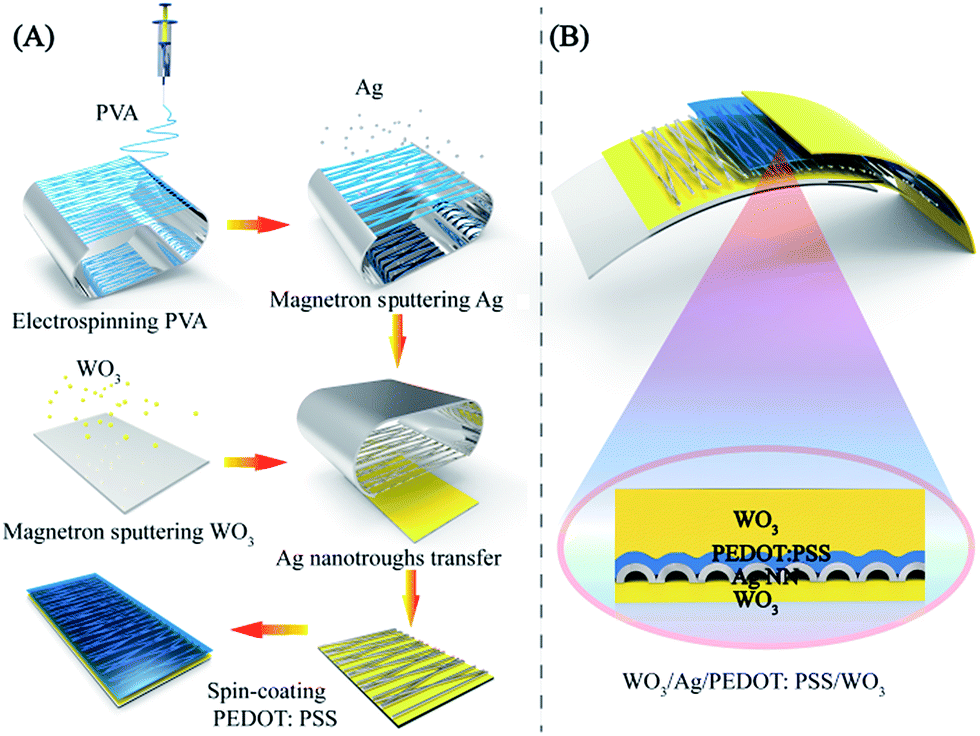 | ||
| Fig. 1 (A) Fabrication procedure of the WO3/Ag NN/PEDOT:PSS transparent electrodes. (B) Schematic illustration of a cross-section of the WO3/Ag NN/PEDOT:PSS/WO3 hybrid EC film. | ||
Deposition of the EC hybrid film
The EC hybrid film was fabricated by magnetron sputtered WO3 coated on the surface of the WO3/Ag NN/PEDOT:PSS hybrid electrode for 10–600 nm by only modulating the sputtering time. The control group was prepared by sputtering WO3 on an original PET/Ag NN substrate with the same parameters.Four kinds of EC device were fabricated for investigating chemical stability, Ag NN/WO3, WO3/Ag NN/WO3, Ag NN/PEDOT:PSS/WO3 and WO3/Ag NN/PEDOT:PSS WO3, on PET substrates.
The mechanical flexibility of the WO3/Ag NN/PEDOT:PSS WO3 hybrid film was investigated on three different substrates (PET, PE cling wrap and PDMS) under bending, twisting and stretching, respectively.
Characterization
The Rs values of the films were measured using a four-point probe (4 Probes Tech RTS-8). The recorded values for Rs were averaged after 6 measurements. Scanning electron microscopy (SEM, Hitachi SU-70) and EDS mapping were used to observe the morphology of the fixed materials. The luminance (Cd m−2) of a green light-emitting diode was simultaneously detected by a Fiber Optic Spectrometer (Ocean Optics syc/syc) at flat and 720° twisted states. An ultraviolet (UV)-visible (VIS)-near-infrared (NIR) spectrophotometer (Perkin Elmer Lambda 750) was utilized to measure the transmittance. All electrochemical measurements were carried out with a three-electrode configuration. The WO3/Ag NN/PEDOT:PSS/WO3 hybrid film served as the working electrode, a platinum (Pt) foil as the counter electrode, a saturated calomel electrode (SCE) worked as the reference electrode, and the electrolyte was 1 M lithium perchlorate (LiClO4) (98%, Aladdin)/propylene carbonate (PC) (99%, Aladdin) solution. The adhesion test (as previously reported by Yang et al.32) was carried out using tape (3 M, 9080, 1 cm width) which was stuck on the surface of the film with finger pressure, and then removed (Fig. S1, ESI†). Mechanical tests such as bending, twisting and stretching were implemented on the WO3/Ag NN/PEDOT:PSS hybrid electrode film, and were all performed using a spiral stand test bench (Handpi HLB).Results and discussion
Characteristics of the hybrid EC electrodes
Fig. 2 displays the morphology and composition of the hybrid electrodes. Before the transferring of the Ag NNs, ultra-thin WO3 was deposited on the transparent PET substrate, which had nearly no effect on transparency (Fig. 2A). Fig. 2B shows a typical example of the Ag NN electrodes where all the nanotroughs are interconnected with each other. The length of the nanotroughs can reach several centimeters (Fig. S2†). The diameter of the Ag networks (200–800 nm) can be simply controlled by adjusting the electrospinning parameters. The enlarged scanning electron microscopy (SEM) image in the inset of Fig. 2B shows the hollow cross-junctional structure of the networks, indicating the dissolution of the PVA nanofibers. The hollow concave shape facilitates transmittance by reducing the electromagnetic cross-section.33 Compared with the bulk-like structure, this hollow NN exhibits excellent conductivity and optical transparence, which can be explained by percolation effects.34 As shown in Fig. 2B–D, the crystalline structure of WO3 cannot be observed and the atomic number ratio of elemental W and O substantially conforms to the ratio of 1:3 in WO3, according to EDX analysis (Fig. S3†). The “X” shaped cross-junctions of the Ag NNs provide uniform interconnections, which lead to the benefits of outstanding mechanical flexibility and stretchability.35 Fig. 2E presents the corresponding energy dispersive spectroscopy (EDS) element mappings of the hybrid film, where uniform sulfur (S) element is stacked on the top and exists in the gaps of Ag NNs, indicating that PEDOT:PSS can only bind to Ag NNs on the substrate. Moreover, compared with single layer Ag NNs, the additional WO3-bottom layer can significantly improve the adhesion between Ag NNs and the substrate, which is verified using the Scotch tape adhesion test (Fig. S1†).
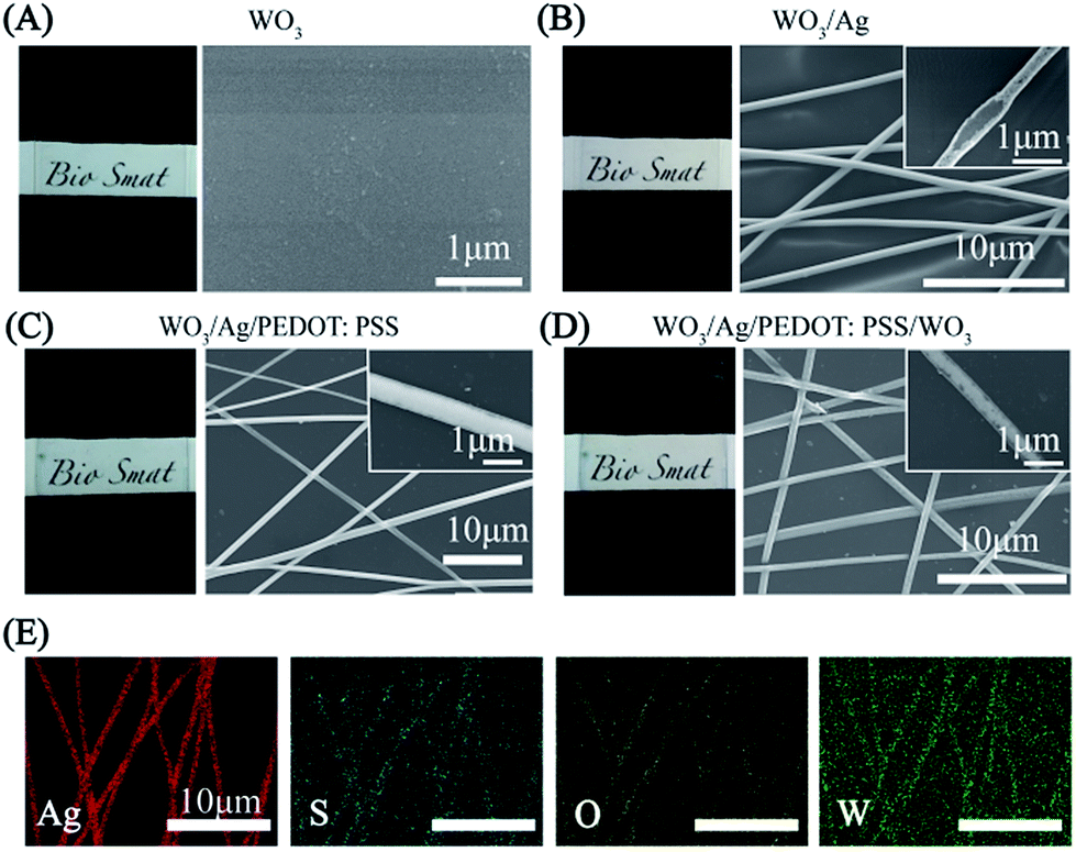 | ||
| Fig. 2 Photographs (left) and corresponding SEM images (right) of the (A) WO3, (B) WO3/Ag NN, (C) WO3/Ag NN/PEDOT:PSS and (D) WO3/Ag NN/PEDOT:PSS/WO3 films. (E) Corresponding EDS element mappings of the WO3/Ag NN/PEDOT:PSS/WO3 hybrid film. | ||
The density of Ag NNs is critical to the optical transparency and electrical conductivity of the hybrid film.36 It is easy to modify the density of Ag NNs by altering the electrospinning parameters and the number of Ag NN layers transferred. Dense Ag NNs provide a uniform, interconnected network which achieves high conductivity with a low Rs, but is harmful to the transparency. Fig. 3A shows the relationship between the optical transmittance of the Ag NN films and their Rs values at a wavelength of 550 nm. Obviously, the transmittance is proportional to the Rs of the Ag NN films below 2.50 Ω sq−1, and then the curve’s growth begins to slow and stabilize. Fig. 3B shows that the transmittance of the hybrid film also increases with enhancing Rs values in the visible range. An Rs of 1.08 Ω sq−1 was achieved at over 85% transparency, and the excellent optical and electrical performance exceeds commonly used ITO, which was verified by the corresponding comparisons of transmittance and Rs values among commercial ITO, the Ag NNs and the WO3/Ag NN, Ag NN/PEDOT:PSS and WO3/Ag NN/PEDOT:PSS hybrid films (Fig. S4†). To investigate the mechanical flexibility of the hybrid electrode, each sample with a size of 2.5 cm × 1 cm was bent to a radius of 0.5 cm and then released to its initial position 5000 times. It is apparent from Fig. 3C that smaller changes in resistance are observed for Ag NNs and hybrid electrodes with 405% and 154% increases, respectively, while ITO suffers from serious damage and its Rs increases sharply until 5152% after bending 5000 times. In Fig. 3C, ΔR/R0 represents the Rs variations obtained during repeated bending, R0 is the initial Rs, ΔR is the difference in the measured Rs after the bending cycles minus R0. It is worth noting that there was only a 54% increase in ΔR/R0 for the hybrid film, and a 305% increase for the Ag NN film, indicating that the additional WO3-bottom and PEDOT:PSS can improve the mechanical flexibility of Ag NNs.
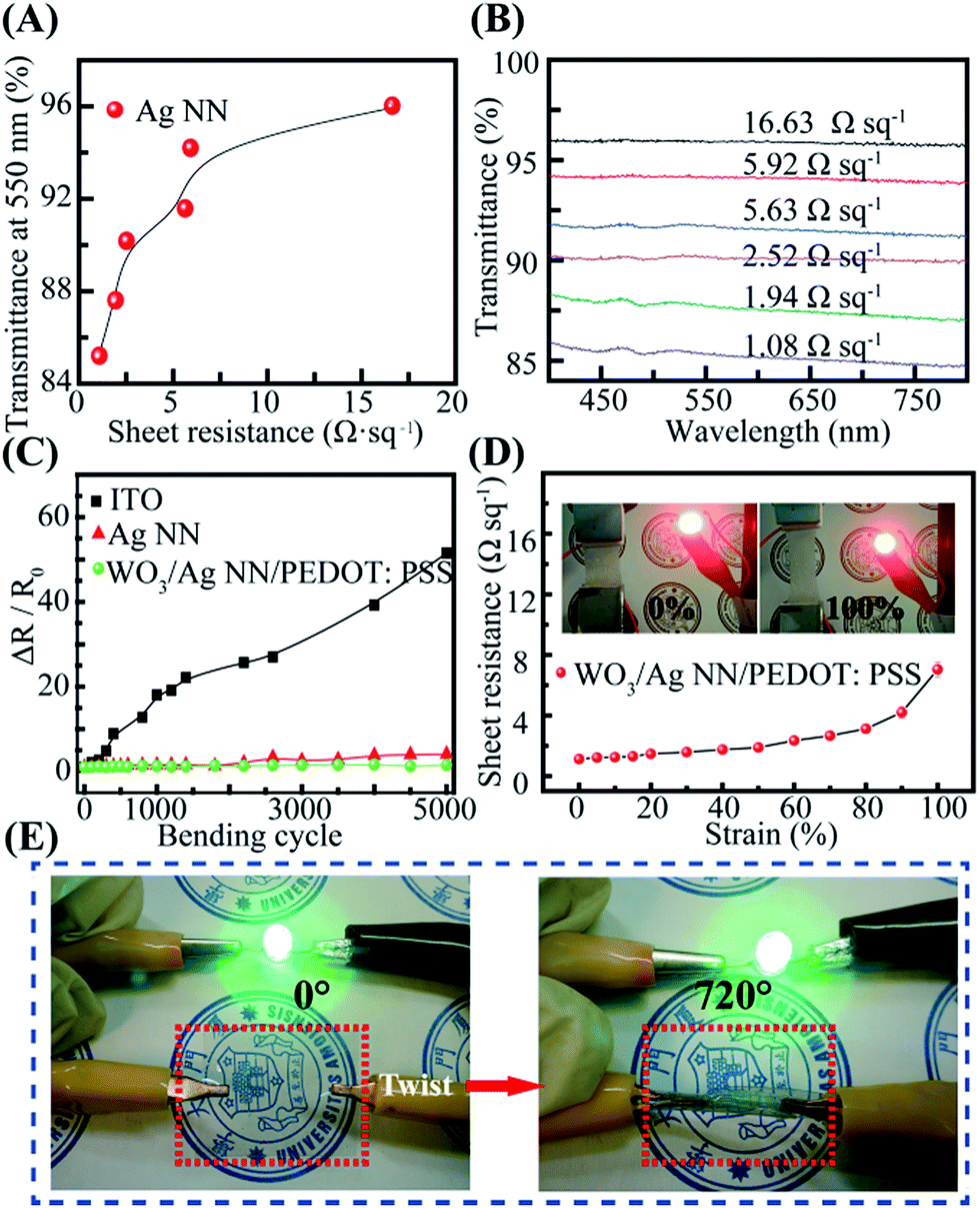 | ||
| Fig. 3 Mechanical stability of the hybrid electrode. (A) The relationship between transmittance at 550 nm and the sheet resistance of the Ag NNs, (B) the visible transmittance spectra of the Ag NNs vs. different Rs values. (C) The mechanical flexibility test of ITO, the Ag NNs and the WO3/Ag NN/PEDOT:PSS hybrid film on a PET substrate after 5000 bending cycles at a radius of 0.5 cm. (D) The Rs values of the WO3/Ag NN/PEDOT:PSS film on Ecoflex as a function of tensile strain. (E) Photographs of the WO3/Ag/PEDOT:PSS/WO3 hybrid film connected in series with a green light-emitting diode when flattened (left) and forcible twisting (right). | ||
Fig. 3D shows the Rs of the hybrid film on an Ecoflex substrate as a function of tensile strain and the insets are photographs of the hybrid electrode on Ecoflex film with different tensile strains. Obviously, Rs increased slowly when the tensile strain increased from 0% to 80%, and adverse effects with cracking of the Ag NNs (Fig. S5†) would follow at above 80% with a sudden change in the curve. The corresponding video of the tensile strain test is provided in the ESI as Video S1,† indicating that the film maintained good electrical conductivity until the tensile strain was larger than 150%. The adhesion property is another critical factor correlated with the stability and durability of the integrated devices. For the hybrid film, the Ag NN layer was coated by ultra-thin WO3-bottom and PEDOT:PSS layers, which could act as protective layers. The Ag NN film without protective layers was readily torn from the PET substrate by scotch tape, whereas the hybrid film maintained integrity. It is notable that the hybrid film maintains good mechanical conductivity, confirmed by connecting it in series with a green light-emitting diode (LED) and lighting up the LED during 720° forcible twisting (Fig. 3E). The 96.6% luminance (Cd m−2) retention demonstrated the mechanical robustness and stability of the hybrid film.
Chemical stability of the hybrid EC film
Cyclic voltammetry (CV) measurements of the hybrid film with a WO3 EC layer were carried out using a three-electrode configuration, as shown in Fig. 4(A and B). The WO3/Ag NN/PEDOT:PSS/WO3 hybrid film, Pt foil and saturated calomel electrode (SCE) served as the working electrode, counter electrode and reference electrode, respectively. The representative peak for WO3 was observed at different potential scan rates from 30 to 100 mV s−1 in the CV curves, which could be attributed to the intercalation (or deintercalation) of Li+ and e− into (or out of) WO3, described as:| xLi+ + xe− + WO3 ↔ LiXWO3. | (1) |
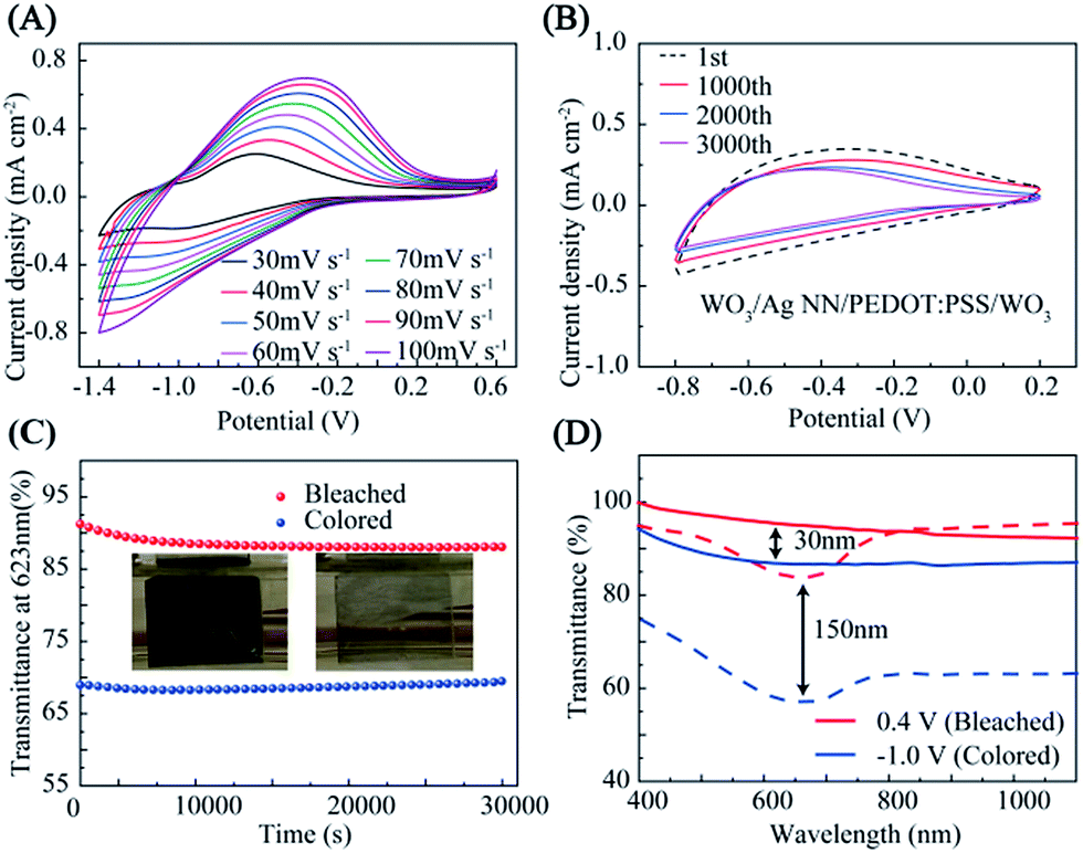 | ||
| Fig. 4 Electrochemical performance of the EC hybrid film. Cyclic voltammograms of the hybrid EC film (A) at different potential scan rates from 30 to 100 mV s−1 and (B) at a scanning rate of 80 mV s−1 in the potential range of −0.8 (colored) to 0.2 V (bleached). (C) Cyclic performance of the hybrid EC film. (D) Transmittance spectra of 30 nm (solid line) and 150 nm (dashed line) at bleached state (0.4 V) and colored state (−1.0 V). | ||
The insertion of Li+ and e− results in a reduction of the W6+ to a lower valence as a W6−x state, leading to the color change of the WO3 EC film to a dark blue color during an applied negative bias potential. On the contrary, the film’s color will fade when a positive bias potential is applied, with the reduced W6−x ions oxidized back due to the extraction of Li+ and e− from the WO3 film. It is a reversible change due to the chemical reaction between oxidized (bleached or transparent) and reduced (colored or dark blue) states. As shown in Fig. 4A, the shifting and deforming of the oxidation and reduction peaks with increasing voltage scan rate is possibly due to ion migration and electron trapping/de-trapping at the interface of the hybrid film in the redox process.37,38
Fig. 4B indicates that the hybrid film has good reversibility, stability and durability in the insertion and extraction of Li+, and the CV curves are displayed at the 1000th, 2000th and 3000th cycle at room temperature, measured in 1 M LiClO4/PC electrolyte. There was a slight decrease during the first 1000 cycles, and then the current density remained stable during 1000–3000 cycles. The EC evaluation of the hybrid film was conducted in a three-electrode configuration by means of an electrochemical workstation with a UV-VIS-NIR spectrometer, as shown in Fig. S6.† The hybrid film presented a noticeable EC phenomenon with an optical modulation of 23% contrast between coloring and bleaching at 623 nm, under a narrow potential range between −1.0 and 0.4 V, when the thickness of the external WO3 was 150 nm. The WO3 on the hybrid electrode sustains 86% of the initial optical contrast after cycling for 30000 s, as shown in Fig. 4C. Digital photographs of WO3 on the hybrid electrode in its bleached state and colored state are shown in the insets of Fig. 4C.
The transmittance modulations of the EC film could be controlled by adjusting the thickness of the external WO3 film. As shown in Fig. 4D, at wavelengths from 300 to 1100 nm, although the sample with 150 nm WO3 exhibits a lower transmittance at the bleached and colored states compared with the 30 nm sample, the optical contrast is twice over that of the 30 nm sample. The transmittance modulations of the devices are directly proportional to the thickness of the WO3 films until a maximum value is reached (∼50%) when the thickness are higher than ∼250 nm, as shown in Fig. S7.†
To investigate the chemical stability of different EC films, transmittances, corresponding with the colored and bleached states of the different films, are displayed in Fig. 5A. It should be noted that without the WO3-bottom layer, the optical contrasts of Ag NN/WO3 and Ag NN/PEDOT:PSS/WO3 were only 0.2% and 11% at the 40th cycle, while those of WO3/Ag NN/WO3 and WO3/Ag NN/PEDOT:PSS/WO3 were 7% and 23%, respectively. Moreover, the Taverage values of bleached state WO3/Ag NN/WO3 and WO3/Ag NN/PEDOT:PSS/WO3 are above 70% and 90%, more than the 65% and 70% obtained for Ag NN/WO3 or Ag NN/PEDOT:PSS/WO3, demonstrating that the presence of the WO3-bottom is beneficial for achieving higher transmittance and better cycling stability and for preventing direct contact between Ag NNs and the substrate. Compared with the WO3/Ag NN/WO3 film, the WO3/Ag NN/PEDOT:PSS/WO3 film sustains a larger optical modulation and subtler degradation, which can be attributed to the PEDOT:PSS layer protecting the Ag NNs from directly contacting the external environment and enhancing adhesion on the substrate.
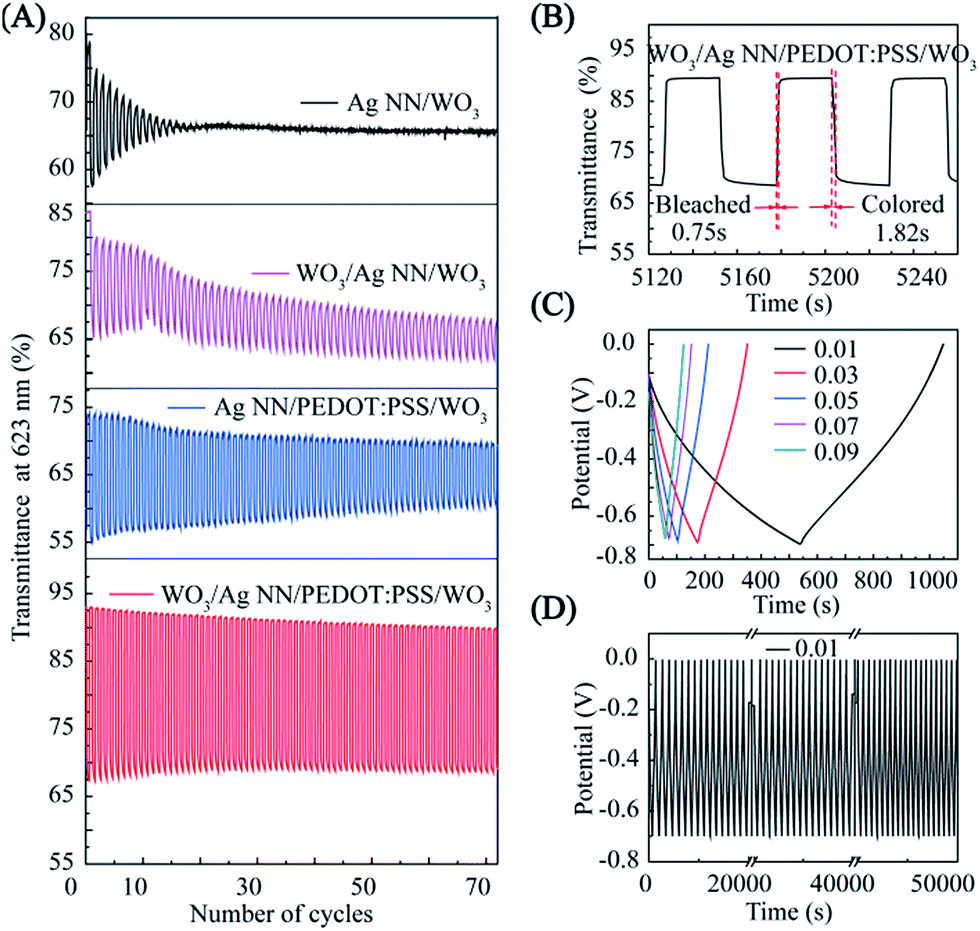 | ||
| Fig. 5 (A) Characterization of the coloring and bleaching rate by measuring the switching time. Statistical results indicate a bleaching time of 0.75 seconds and coloring time of 1.82 seconds. Galvanostatic charge/discharge profile at (C) current densities from 0.01 to 0.1 mA cm−2, and (D) 0.01 mA cm−2. | ||
Apart from optical contrast and cycling life, obtaining switching times between colored states and bleached states under commutative potential is also critical for evaluating the kinetic performance of the ECDs.39 The switching time is defined as the time required for the integrated device to reach 90% of the transmittance change between the steady bleached and colored states.31 For the WO3/Ag NN/PEDOT:PSS/WO3 hybrid film, the switching times, as shown in Fig. 5B, are 0.75 and 1.82 s for bleaching and coloration, respectively, which is faster than Lee’s group (4 and 1 s, respectively)6 and Cai et al. (2.8 and 1.9 s, respectively),3 with EC films based on a Ag NW conductor and an electrodeposited WO3 EC layer.
As we know, the intercalation (or deintercalation) of ions and electrons into (or out of) WO3 during the coloration (or bleaching) process can correspond exactly to the charging (or discharging) process of supercapacitive behavior, as described in eqn (1).3,40 That is to say, the reversible color variation of an ECD can simultaneously monitor its level of stored energy.41,42 The functional ECD must be adequately fast for observation with highly transparent conductive, stable and durable electrodes as the current collector, especially at high current charging/discharging processes. To this end, an electrochromic-supercapacitor (EC-SC) can be designed to simultaneously realize transmittance adjustment and energy storage.43,44 Fig. 5C and D display the charge/discharge curves at different current densities and the corresponding long-term stability test of the EC-SC. The downward lines correspond with the charging and the upward lines with the discharging processes. Charging is related to the intercalation of Li+ and e− into the WO3 film, with a subsequently observed change to dark blue color attributed to the reduction of W6+ ions to W6−x ions, and the discharging process corresponds to the oxidation of the W6−x ions with color bleaching. The specific capacitance (C, mF cm−2) can be calculated as follows:45
 | (2) |
000 s, indicating the stability of the capacitor’s performance under prolonged charging/discharging processes, as shown in Fig. 5D.
Mechanical robustness of the hybrid EC film
Cling wrap is a common thin plastic film typically used for sealing items in containers to keep them fresh over a longer period of time, which is ultra-thin, highly flexible, sold in rolls in boxes with a low price and is easy to access. Constructing EC films on cling wrap is more suitable for developing highly flexible and ultra-thin ECDs which can be stuck on the glass of cars or buildings for reducing energy consumption, or for developing color-changing e-skin (as shown at the top of Fig. 6B), rather than replacement with exorbitant EC smart windows. Here, we successfully fabricate the hybrid EC film on cheap household PE cling wrap, as shown in Fig. 6(A and B). Fig. 6C illustrates that the ultra-thin EC film on PE cling wrap substrate maintains stable and reversible color changes between bleached and colored states after strong repeated kneading (Video S2, ESI†), indicating excellent mechanical robustness. A real-time switching test from the “ON” (bleached) to the “OFF” (colored) state of the “XMU” patterned EC hybrid film during bending at a repeatedly applied voltage between VON (0.4 V) and VOFF (−1 V) was carried out, and the period was 5 s. This was to verify that the EC film exhibits good electrochemical stability during bending and is demonstrated in the ESI (Video S3 and Fig. S8).†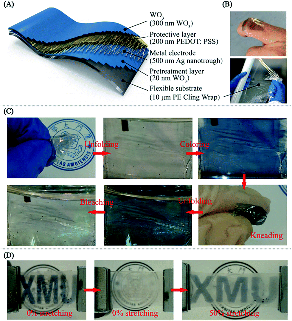 | ||
| Fig. 6 Mechanical robustness of the hybrid EC films on PE cling wrap and PDMS film. (A) Schematic illustration of the structure of the PE cling wrap-based hybrid EC film. (B) The color-changing e-skin (EC film) on one finger (top), and PE cling wrap (bottom). (C) Upon folding and strong kneading, the PE-based hybrid EC film still displays the ability of coloring and bleaching, indicating excellent mechanical flexibility. (D) With 50% tensile strain stretching, the hybrid EC film on a PDMS substrate could also sustain its mechanical stability and electrochromic properties. | ||
The tensile strain tests for the “XMU” patterned hybrid EC film on a flexible PDMS substrate are shown in Fig. 6D. In the first step, the device was in the colored state without any strain and then the logo “XMU” disappeared (bleached) after the application of a positive voltage (0.4 V). Then, 50% tensile strain was applied on the patterned EC film using a spiral stand test bench, inverse voltage was applied and the logo appeared again. The corresponding SEM images, as shown in Fig. S5,† indicate that the Ag NNs in the patterned hybrid EC film remain intact while the continuous WO3 layer is fractured during stretching, demonstrating the unique hollow cross-junctional structure of the TCE, which can bear stretching and bending to support the working of the ECD. The WO3/Ag NN/PEDOT:PSS EC hybrid film, which was successfully constructed on the different PET, cling wrap and PDMS flexible substrates with resounding mechanical flexibility, stability and EC performance, could be a strikingly attractive candidate for flexible and wearable electronic applications.
Conclusions
In conclusion, a flexible sandwiched WO3/Ag NN/PEDOT:PSS electrode was successfully fabricated which simultaneously displays prominent conductivity (sheet resistance as low as 1.08 Ω sq−1) and transparency (85%). It was further revealed that this electrode can adhere tightly to WO3, together forming a flexible electrochromic device. This ECD is not only extremely flexible upon mechanical bending, twisting, stretching and even strong kneading, but also preserves excellent cycling stability. In addition, this ECD also possesses advantages such as rapid switching time (0.75 s for bleaching and 1.82 s for coloring) and 86% retention of optical contrast even after 30000 s cycling. On the other hand, we also confirmed that our electrode can be fabricated on various flexible substrates such as PE, PDMS and Ecoflex. Our work provides new opportunities for the next generation of flexible and wearable electronic applications on various flexible substrates such as PE, PDMS and Ecoflex. Furthermore, a considerable application prospect in energy storage, such as in a supercapacitor with an extraordinary charging/discharging stability that can sense changes using color mutation, is demonstrated.
Conflicts of interest
There are no conflicts to declare.Acknowledgements
This work was supported by the National Natural Science Foundation of China (No. 51502253, U1405226), the Guangdong Natural Science Foundation (2016A030310369), the Fujian Natural Science Foundation (No. 2017J01104), the Fundamental Research Funds for the Central Universities of China (No. 20720180013), the “111” Project (B16029), the Doctoral Fund of the Ministry of Education (20130121110018) and the 1000 Talents Program funding from the Xiamen university.References
- X. Pu, M. M. Liu, X. Y. Chen, J. M. Sun, C. H. Du, Y. Zhang, J. Y. Zhai, W. G. Hu and Z. L. Wang, Sci. Adv., 2017, 3, e1700015 CrossRef PubMed.
- B. Han, K. Pei, Y. L. Huang, X. J. Zhang, Q. K. Rong, Q. G. Lin, Y. F. Guo, T. Y. Sun, C. F. Guo, D. Carnahan, M. Giersig, Y. Wang, J. W. Gao, Z. F. Ren and K. Kempa, Adv. Mater., 2014, 26, 873–877 CrossRef PubMed.
- G. F. Cai, P. Darmawan, M. Q. Cui, J. X. Wang, J. W. Chen, S. Magdassi and P. S. Lee, Adv. Energy Mater., 2016, 6, 1501882 CrossRef.
- S. Park, K. Parida and P. S. Lee, Adv. Energy Mater., 2017, 7, 1701369 CrossRef.
- R. Baetens, B. P. Jelle and A. Gustavsen, Sol. Energy Mater. Sol. Cells, 2010, 94, 87–105 CrossRef.
- C. Y. Yan, W. B. Kang, J. X. Wang, M. Q. Cui, X. Wang, C. Y. Foo, K. J. Chee and P. S. Lee, ACS Nano, 2014, 8, 316–322 CrossRef PubMed.
- C. Lee, Y. Oh, I. S. Yoon, S. H. Kim, B. K. Ju and J. M. Hong, Sci. Rep., 2018, 8, 2763 CrossRef PubMed.
- J. Jensen and F. C. Krebs, Adv. Mater., 2014, 26, 7231–7234 CrossRef PubMed.
- K. R. Li, Q. H. Zhang, H. Z. Wang and Y. G. Li, J. Mater. Chem. C, 2016, 4, 5849–5857 RSC.
- W. Liu, M. S. Song, B. Kong and Y. Cui, Adv. Mater., 2017, 29, 1603436 CrossRef PubMed.
- G. D. Zhou, Y. Q. Yao, Z. S. Lu, X. D. Yang, J. J. Han, G. Wang, X. Rao, P. Li, Q. Liu and Q. L. Song, Nanotechnology, 2017, 28, 425202 CrossRef PubMed.
- G. D. Zhou, Y. Q. Yao, X. S. Zhao, X. Q. Liu, B. Sun and A. K. Zhou, RSC Adv., 2016, 6, 59370–59374 RSC.
- A. Pierre, I. Deckman, P. B. Lechene and A. C. Arias, Adv. Mater., 2015, 27, 6411–6417 CrossRef PubMed.
- P. M. Beaujuge and J. R. Reynolds, Chem. Rev., 2010, 110, 268–320 CrossRef PubMed.
- P. C. Hsu, S. Wang, H. Wu, V. K. Narasimhan, D. S. Kong, H. R. Lee and Y. Cui, Nat. Commun., 2013, 4, 2522 CrossRef PubMed.
- T. F. Qiu, B. Luo, M. H. Liang, J. Ning, B. Wang, X. L. Li and L. J. Zhi, Carbon, 2015, 81, 232–238 CrossRef.
- G. D. Zhou, L. H. Xiao, S. J. Zhang, B. Wu, X. Q. Liu and A. K. Zhou, J. Alloys Compd., 2017, 722, 753–759 CrossRef.
- G. D. Zhou, S. K. Duan, P. Li, B. Sun, B. Wu, Y. Q. Yao, X. D. Yang, J. J. Han, J. G. Wu and G. Wang, Adv. Electron. Mater., 2018, 1700567 CrossRef.
- J. Z. Chen, W. Y. Ko, Y. C. Yen, P. H. Chen and K. J. Lin, ACS Nano, 2012, 6, 6633–6639 CrossRef PubMed.
- L. Liang, J. J. Zhang, Y. Y. Zhou, J. F. Xie, X. D. Zhang, M. L. Guan, B. C. Pan and Y. Xie, Sci. Rep., 2013, 3, 1936 CrossRef PubMed.
- G. D. Zhou, W. X. Zhao, X. Q. Ma and A. K. Zhou, J. Alloys Compd., 2016, 679, 47–53 CrossRef.
- W. X. Guo, Z. J. Xu, F. Y. Zhang, S. Y. Xie, H. Y. Xu and X. Y. Liu, Adv. Funct. Mater., 2016, 26, 8855–8884 CrossRef.
- S. S. Yao and Y. Zhu, Adv. Mater., 2015, 27, 1480–1511 CrossRef PubMed.
- W. F. Zhang, B. F. Zhao, Z. C. He, X. M. Zhao, H. T. Wang, S. F. Yang, H. B. Wu and Y. Cao, Energy Environ. Sci., 2013, 6, 1956–1964 Search PubMed.
- M. Aleksandrova, V. Videkov, R. Ivanova, A. K. Singh and G. S. Thool, Mater. Lett., 2016, 174, 204–208 CrossRef.
- Y. C. Tseng, A. U. Mane, J. W. Elam and S. B. Darling, Sol. Energy Mater. Sol. Cells, 2012, 99, 235–239 CrossRef.
- Y. J. Noh, S. S. Kim, T. W. Kim and S. I. Na, Sol. Energy Mater. Sol. Cells, 2014, 120, 226–230 CrossRef.
- Y. S. Kim, M. H. Chang, E. J. Lee, D. W. Ihm and J. Y. Kim, Synth. Met., 2014, 195, 69–74 CrossRef.
- X. D. Wang, Y. F. Zhang, X. J. Zhang, Z. H. Huo, X. Y. Li, M. L. Que, Z. C. Peng, H. Wang and C. F. Pan, Adv. Mater., 2018, 30, 1706738 CrossRef PubMed.
- W. B. Kang, M. F. Lin, J. W. Chen and P. S. Lee, Small, 2016, 12, 6370–6377 CrossRef PubMed.
- P. J. Yao, S. Y. Xie, M. D. Ye, R. Yu, Q. Liu, D. D. Yan, W. W. Cai, W. X. Guo and X. Y. Liu, RSC Adv., 2017, 7, 29088–29095 RSC.
- R. Zhu, C. H. Chung, K. C. Cha, W. B. Yang, Y. B. Zheng, H. P. Zhou, T. B. Song, C. C. Chen, P. S. Weiss, G. Li and Y. Yang, ACS Nano, 2011, 5, 9877–9882 CrossRef PubMed.
- H. Wu, D. S. Kong, Z. C. Ruan, P. C. Hsu, S. Wang, Z. F. Yu, T. J. Carney, L. B. Hu, S. H. Fan and Y. Cui, Nat. Nanotechnol., 2013, 8, 421–425 CrossRef PubMed.
- S. De and J. N. Coleman, MRS Bull., 2011, 36, 774–781 CrossRef.
- B. W. An, E. J. Gwak, K. Kim, Y. C. Kim, J. Jang, J. Y. Kim and J. U. Park, Nano Lett., 2016, 16, 471–478 CrossRef PubMed.
- T. C. Wang, L. J. Chang, S. Kong, S. Yang, Y. Jia and C. P. Wong, Monatsh. Chem., 2014, 145, 61–64 CrossRef.
- G. D. Zhou, B. Sun, Y. Q. Yao, H. H. Zhang, A. K. Zhou, K. Alameh, B. F. Ding and Q. L. Song, Appl. Phys. Lett., 2016, 109, 143904 CrossRef.
- G. D. Zhou, Z. S. Lu, Y. Q. Yao, G. Wang, X. D. Yang, A. K. Zhou, P. Li, B. F. Ding and Q. L. Song, J. Appl. Phys., 2017, 121, 155302 CrossRef.
- A. Kim, Y. Won, K. Woo, C.-H. Kim and J. Moon, ACS Nano, 2013, 7, 1081–1091 CrossRef PubMed.
- M. S. Zhu, W. J. Meng, Y. Huang, Y. Huang and C. Y. Zhi, ACS Appl. Mater. Interfaces, 2014, 6, 18901–18910 Search PubMed.
- Z. J. Bi, X. M. Li, Y. B. Chen, X. K. Xu, S. D. Zhang and Q. X. Zhu, Electrochim. Acta, 2017, 227, 61–68 CrossRef.
- X. H. Lu, T. Zhai, X. H. Zhang, Y. Q. Shen, L. Y. Yuan, B. Hu, L. Gong, J. Chen, Y. H. Gao, J. Zhou, Y. X. Tong and Z. L. Wang, Adv. Mater., 2012, 24, 938–944 CrossRef PubMed.
- Y. Huang, M. S. Zhu, Y. Huang, Z. X. Pei, H. F. Li, Z. F. Wang, Q. Xue and C. Y. Zhi, Adv. Mater., 2016, 28, 8344–8364 CrossRef PubMed.
- Y. Huang, Y. Huang, W. J. Meng, M. S. Zhu, H. T. Xue, C. S. Lee and C. Y. Zhi, ACS Appl. Mater. Interfaces, 2015, 7, 2569–2574 Search PubMed.
- T. G. Yun, D. Kim, Y. H. Kim, M. Park, S. Hyun and S. M. Han, Adv. Mater., 2017, 29, 1606728 CrossRef PubMed.
Footnotes |
| † Electronic supplementary information (ESI) available. See DOI: 10.1039/c8ra02829j |
| ‡ These authors contributed equally to this work. |
| This journal is © The Royal Society of Chemistry 2018 |