
 Open Access Article
 This Open Access Article is licensed under a Creative Commons Attribution-Non Commercial 3.0 Unported Licence
Structural study of epitaxial NdBa2Cu3O7−x films by laser chemical vapor deposition
Rong Tu a,
Kaidong Wanga,
Ting Wanga,
Meijun Yanga,
Qizhong Lib,
Song Zhang*a,
Lianmeng Zhanga,
Takashi Gotoac,
Ji Shiad and
Hitoshi Ohmoriae
a,
Kaidong Wanga,
Ting Wanga,
Meijun Yanga,
Qizhong Lib,
Song Zhang*a,
Lianmeng Zhanga,
Takashi Gotoac,
Ji Shiad and
Hitoshi Ohmoriae
aState Key Laboratory of Advanced Technology for Materials Synthesis and Processing, Wuhan University of Technology, 122 Luoshi Road, Wuhan 430070, People's Republic of China. E-mail: kobe@whut.edu.cn; superkobe0104@gmail.com
bHubei Key Laboratory of Advanced Technology for Automotive Components, Wuhan University of Technology, Wuhan 430070, China
cInstitute for Materials Research, Tohoku University, 2-1-1 Katahira, Aoba-ku, Sendai 980-8577, Japan
dSchool of Materials and Chemical Technology, Tokyo Institute of Technology, Tokyo 152-8552, Japan
eInstitute of Physical and Chemical Research, 2-1 Hirosawa, Wako, Saitama 351-0198, Japan
First published on 30th May 2018
Abstract
Epitaxial NdBa2Cu3O7−x films were prepared on (100) LaAlO3 single crystal substrates by laser chemical vapor deposition (laser CVD). The effect of deposition temperature on preferred orientation, crystallinity, microstructure, deposition rate of films was investigated. The preferred orientation of the NdBCO films changed from a, c-axis to c-axis, then back to a, c-axis, as the deposition temperature was increased from 993 to 1093 K. The highly c-axis-oriented epitaxial NdBa2Cu3O7−x film with critical transition temperature of 87 K was obtained at Tdep = 1033 K, with the in-plane epitaxial orientation relationship of NdBCO [100]∥LAO [010] and NdBCO [010]∥LAO [001]. The growth orientation varied from a-axis to c-axis as the film thickness increased in the case of the a, c-co-oriented NdBCO film. The contribution of thickness-dependent strain relaxation to preferred orientation of the NdBCO films was also discussed.
1. Introduction
Since the discovery of high temperature superconductivity in REBCO (RE = rare earth element) family materials, NdBa2Cu3O7−x (NdBCO) has attracted extensive attention for its high critical temperature (Tc) and critical current density (Jc).1–3 Meanwhile, NdBCO films were also reported for the distinct advantages of better crystallinity and higher surface stability over YBa2Cu3O7−x (YBCO) films, enabling multilayers with excellent epitaxial quality.4–6For NdBCO crystal, critical current along the ab-plane is far superior to that along the c-axis, because of the difference between the coherent length (ξ) along the ab-plane (1.5–2 nm) and the c-axis (0.2–0.3 nm) of NdBCO.7 Therefore, c-axis-oriented and well ab-aligned NdBCO film possesses high-ranking superconducting properties. As a matter of fact, c-axis-oriented epitaxial growth of NdBCO films has been studied under the cases of various fabrication techniques, including metal organic chemical vapor deposition (MOCVD),8,9 pulsed laser deposition (PLD),10,11 magnetron sputtering.12–14 These studies supposed that the deposition temperature (Tdep) was the key factor affecting the growth orientation, and as the film thickness increased, the strain relaxation in the film would also have a certain effect on the growth orientation. However, the contributions of Tdep and thickness-dependent strain relaxation on microstructure of c-axis-oriented epi-layers were not fully understood.
We adopted laser chemical vapor deposition technique (laser CVD)15–17 to fabricate NdBCO films by continuously introducing a fixed-wavelength laser beam with high energy density. Laser CVD is able to prepare film at sufficiently high deposition rates with significant orientation.18–21 The laser beam not only has a simple heating effect, but also can induce decomposition of the metal organic precursors and decrease the activation energy of chemical reaction occurring on the substrate.22,23
In this study, we prepared epitaxial NdBCO films by laser CVD. The effect of deposition temperature (Tdep) on preferred orientation, crystallinity, microstructure, deposition rate and the effect of thickness-dependent strain relaxation on preferred orientation of the NdBCO films were investigated.
2. Experimental
A schematic of laser CVD apparatus is depicted in Fig. 1. The NdBCO films were grown on (100)-oriented LAO single-crystal substrates (5.0 mm × 10.0 mm × 0.5 mm, Hefei Kejing Inc., China). The source materials were Nd(DPM)3, Ba(DPM)2, Cu(DPM)2 (Toshima Manufacturing Co. Ltd., Japan), where DPM represents dipivaloyl-methanate, all of which were loaded into three individual sealed heaters. The gas pipelines were equipped with the heating zones for controlling temperature to prevent the condensation of source gas. The LAO substrate was first ultrasonically cleaned in alcohol for 20 minutes and blown dry with nitrogen gas and placed on a substrate holder in the chamber. Then, the LAO substrate was preheated via laser irradiation at 873 K for 1800 s after deposition chamber was evacuated to 50 Pa. Nd(DPM)3, Ba(DPM)2, Cu(DPM)2 were vaporized at the temperature of 478, 576, 443 K and introduced into the chamber by Ar gas (≥99.999%, Wuhan Minghui Inc., China) at the flow rate of 100, 120, 80 sccm, respectively. O2 gas (≥99.995%, Wuhan Minghui Inc., China) was introduced into the chamber as the reactant gas at the flow rate of 400 sccm during the deposition. The total pressure (Ptot) in chamber was fixed at 700 Pa. The deposited region was irradiated by IR-laser (LHTC-200, Beijing ZK laser, China) with a wavelength of 808 nm at the angle of 45° during the deposition. The Tdep was 993–1093 K by controlling the laser power, and measured by an infrared pyrometer (CT laser, Optris, Berlin, Germany). The deposition time was 600 s. The distance between the nozzle and the substrate was 50 mm. After deposition, The NdBCO film was heat-treated at 673 K for 3600 s in O2 atmosphere (100 kPa).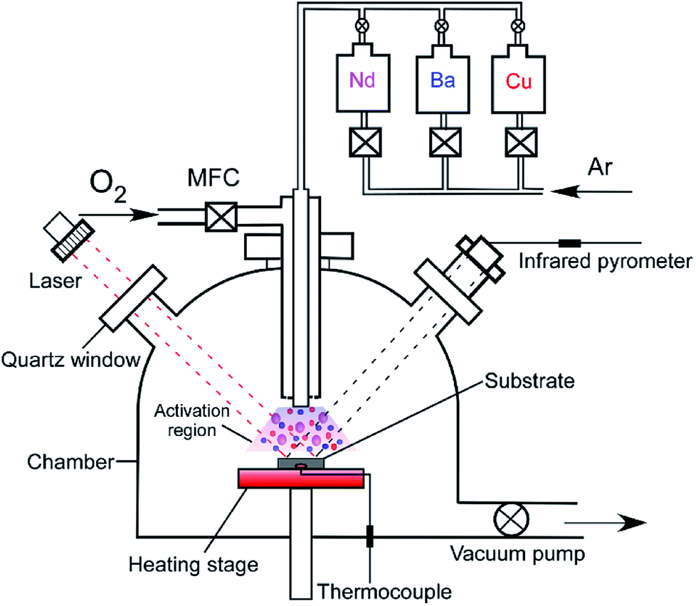 | ||
| Fig. 1 A schematic of laser CVD apparatus. | ||
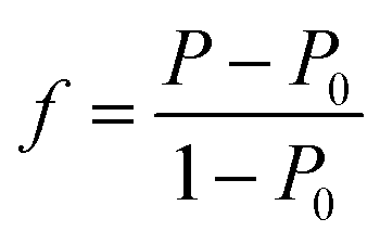
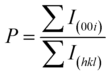
The crystal phases, out-plane and in-plane orientation of the deposited films were examined by X-ray diffraction (XRD) using an attachment for pole figures (Rigaku Ultima III, Tokyo, Japan; 40 kV, 40 mA) with Cu-Kα radiation (wavelength = 0.15406 nm). The degree of the c-axis preferred orientation (f) of the NdBCO films was calculated by using the Lotgering formula as shown as eqn(1):24
 | (1) |
 and
and 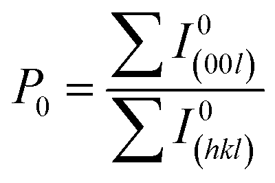 . P represents the ratio of the XRD intensity of all the (00l) peaks to the XRD intensity of all the (hkl) peaks of the NdBCO films from 5° to 80°. P0 represents the corresponding ratio of the random-oriented NdBCO bulk (JCPDS #89-5734). The crystallinity of NdBCO film was evaluated from the full-width at half-maximum (FWHM) of the φ-scan on the (116) reflection. The film composition was analyzed by X-ray photoelectron spectroscopy (XPS, Escalab 250Xi, Thermo fisher scientific, USA). After Shirley-type background subtraction, the raw XPS spectrums were fitted for quantification analysis. Deposition rate (Rdep) was calculated from the thickness and deposition time. The schematic diagram of the crystal growth relationship was drawn by VESTA software (Ver.3.1.0, 64-bit edition). The microstructure of NdBCO films was observed by a field emission scanning electron microscopy (FESEM, FEI Quanta-250, 20 kV, USA). The electron diffraction and high resolution lattice fringe of deposited film, and interface between the film and substrate were observed by transmission electron microscopy (TEM, JEOL JEM-2100, 200 kV; Tokyo, Japan). The temperature dependence of electrical resistivity (R) of the NdBCO films was measured with a standard four-point-probe using a physical property measurement system (PPMS9, Quantum Design, USA) in the range of 10–300 K. The c-axis lattice parameters of the c-axis-oriented NdBCO grains were obtained from the Maud refinement analysis on the diffraction data from the experimental results.
3. Results and discussion
Fig. 2(a) shows XRD patterns in logarithmic scale of the NdBCO films prepared on the LAO at Tdep = 993–1093 K. Temperature had a significant influence on the growth orientation of the films. The variation of growth orientation with temperature can be divided into three stages. At the first stage from 993 to 1013 K, NdBCO films with a mixture of a-axis and c-axis orientation were prepared. c-Axis-oriented NdBCO films were obtained at the second stage (1033 K), due to the sufficient energy provided for atomic migration to form c-axis configuration. With temperature increasing to the third stage (1053–1093 K), NdBCO films showed a, c-axis-co-oriented again and the impurity phase of Ba2CuO3 appeared at Tdep = 1053 K. This trend of orientation change is different from the ones reported in the former documents that growth orientation would change monotonously from a-axis to c-axis with increasing temperature.11,25–27 The possible reason of this phenomenon is that the laser with higher output power causes more intense collisions of the gas reactant molecules in the laser radiation zone, resulting in a significant decrease in the energy of the deposited atoms. As a result, a-axis-oriented grains would appear because of the insufficient atomic migration. Fig. 2(b) further quantitatively describes this change trend of NdBCO films growth orientation. At Tdep = 993–1033 K, f for the c-axis increased from 0.39 to 1.00, suggesting a fully c-axis-oriented NdBCO film formed. Then, f for the c-axis declined and remained almost unchanged near f = 0.50 in the temperature range from 1053 to 1093 K. These results indicate that the c-axis-oriented NdBCO films can only be stably prepared at a strictly limited temperature range of 1033 to 1053 K for laser CVD. Fig. 2(c) shows the temperature dependence of the FWMH of the φ-scan on the (116) reflection prepared at Tdep = 993–1093 K. As it was shown in Fig. 2(c), the FWHM value of the φ-scan firstly decreased from 2.20° to 0.91° in the range of 993–1033 K and then increased to 1.82° with increasing Tdep to 1093 K. The lowest FWHM value was 0.91° at Tdep = 1033 K. Combined with the result of the XRD patterns (Fig. 2(a)), it indicates that the NdBCO film of c-axis orientation possesses the highest crystal quality.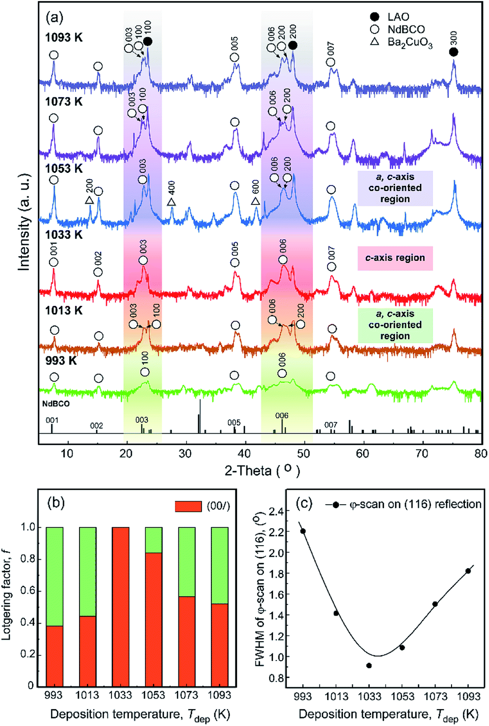 | ||
| Fig. 2 Characterization of the effect of Tdep on the structure of NdBCO films prepared at Tdep = 993–1093 K. (a) XRD patterns of the NdBCO films. (b) The degree of c-axis orientation of the NdBCO films as a function of Tdep. (c) FWHM of φ-scan on the (116) reflection of NdBCO film as a function of Tdep. | ||
This trend of temperature dependence of growth orientation can be demonstrated by the growth models of the NdBCO films under different cases as shown in Fig. 3. Considering the atomic arrangement of the crystal, the ideal surface of the c-axis-oriented grains (i.e., (00l) plane) can only accommodate one specific layer of a single cation (Re, Ba, Cu) due to the characteristic of two-dimensional layered structure of REBCO.28 Therefore, as shown in Fig. 3(a), the deposited atoms have to migrate over a long distance to occupy the specific position for c-axis growth, which is considered more stable than a-axis growth thermodynamically. In contrast, the surface of the a-axis grains can accommodate any elements Re, Ba, Cu and O without much migration so that a-axis grains are more easily formed in the aspect of kinetics (shorter migration distance: Fig. 3(b)). Consequently, the control of the crystal growth orientation is actually a matter of the regulation of the thermodynamics and kinetics factors, which means that a-axis-oriented films can be grown at a lower energy and c-axis-oriented ones need higher migration energy for crystallization.29 Meanwhile, the laser with excessive power density would not only cause the violent collisions of the gas molecules, but also the damage of the surface condition, such as steps, etch pits and micro-cracks, resulting in the a-axis-oriented grains.30,31
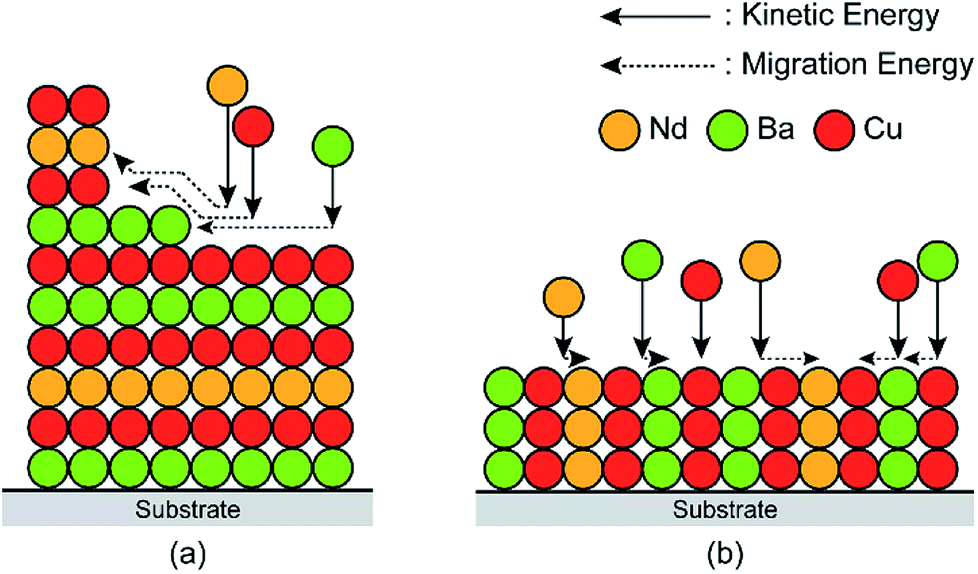 | ||
| Fig. 3 The surface migration models in the case of (a) c-axis- and (b) a-axis-oriented NdBCO films. | ||
Fig. 4 shows the pole figures from the (116) reflection of the NdBCO films prepared at Tdep = 1033 K and 1053 K, and those from the (111) reflection of the LAO substrate. The epitaxial relationships between these two NdBCO films and LAO substrate are depicted in Fig. 4(b) and (d), respectively. The pole figure from the (116) reflection of the NdBCO film prepared at Tdep = 1033 K exhibits a fourfold pattern at an elevation angle (α) of 55° (Fig. 4(a)), which was attributed to the NdBCO {116} planes with a complementary angle of 35° to the NdBCO (001) plane. Furthermore, there was no any other peaks identified in the pole figure, suggesting a fully c-axis-oriented NdBCO film. The azimuth angles (β) of the four reflections of the NdBCO (116) plane were identical to those of the LAO (111) plane, indicating the epitaxial relationship of NdBCO [100]∥LAO [010] and NdBCO [010]∥LAO [001] for the c-axis-oriented NdBCO films, as shown in Fig. 4(b).
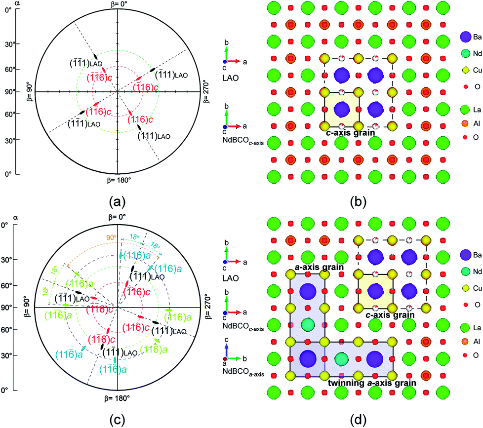 | ||
| Fig. 4 Pole figure patterns of the (116) reflection of NdBCO films prepared at Tdep = 1033 K (a) and 1053 K (c), and those of the (111) reflection of the LAO substrate. Schematic diagram (b) and (d) are their epitaxial relationship of NdBCO films and LAO substrate, respectively. ((116)c-axis denotes planes from c-axis-oriented grains, (116)a-axis denotes planes from a-axis-oriented grains). | ||
The pole figure from the (116) reflections of the NdBCO film prepared at Tdep = 1053 K exhibits a fourfold pattern at approximately α = 55°, and two sets of identical fourfold pattern at approximately α = 24° with an azimuthal angular rotation of 90° from each other (Fig. 4(c)). The fourfold pattern at α = 55° originated from the c-axis-oriented NdBCO grains and was attributed to the NdBCO {116} planes with a complementary angle of 35° to the NdBCO (001) plane. The two sets of identical fourfold pattern at α = 24° originated from the a-axis-oriented NdBCO grains and were attributed to the NdBCO {116} planes with a complementary angle of 66° to the NdBCO (001) plane. The fourfold pattern of the NdBCO {116} planes appeared twice, with a repeating angle of 90°, which was ascribed to a 90° twinning structure of a-axis-oriented grains.32 Each pole of the NdBCO {116} planes had an azimuth angle (β) of 18° from its adjacent LAO {111} plane pole. This result is in agreement with the calculated azimuth angle between the pole of the LAO (111) plane in the [100] projection and that of the NdBCO (116) plane in the [100] projection.32 Therefore, both b- and c-axis of the a-axis-oriented NdBCO grains were aligned with those of the LAO substrate. Accordingly, a schematic diagram of epitaxial relationship of the a, c-axis-co-oriented NdBCO films and the LAO substrate is proposed in Fig. 4(d), where the 90° twinning relationship is also presented.
Fig. 5 shows surface and cross-section secondary electron images of the NdBCO films prepared at Tdep = 993–1093 K. The film prepared at Tdep = 993 K shows many discrete particulates because of the insufficient energy for atoms migration, revealing the typical island growth mode. With increasing Tdep to 1013 K, the film becomes continuous with rectangular outgrowth particles, identified as a-axis grains.33 This is due to faster growth of NdBCO along the a-axis than the c-axis.34 The film deposited at Tdep = 1033 K shows a uniform dense surface morphology, indicating the layer growth mode. According to the result of XRD patterns (Fig. 2(a)), this is attributed to the fully c-axis-oriented NdBCO film. The Nd![[thin space (1/6-em)]](https://www.rsc.org/images/entities/char_2009.gif) :Ba and Nd:Cu ratios of the NdBCO film were estimated, by the XPS quantification analysis, to be 1:2.13 and 1:2.71, respectively. The ratios were close to the standard stoichiometric ratios of NdBCO films. At Tdep = 1053 K, the film exhibits a terraced surface with a few holes. The a-axis grains of NdBCO films deposited at Tdep = 1073 K and 1093 K shows two distinctive shape characteristics: the isolated rectangular ones with regular arrangement along the axes of the underlying LAO template and the elongated ones with random orientation, suggesting that increasing temperature would cause change of in-plane orientation of a-axis grains. The growth rates of the films from 993–1093 K are between 3.6–22.2 μm h−1 according to the cross-section secondary electron images. Also, the corresponding growth modes are demonstrated in Fig. 5.
:Ba and Nd:Cu ratios of the NdBCO film were estimated, by the XPS quantification analysis, to be 1:2.13 and 1:2.71, respectively. The ratios were close to the standard stoichiometric ratios of NdBCO films. At Tdep = 1053 K, the film exhibits a terraced surface with a few holes. The a-axis grains of NdBCO films deposited at Tdep = 1073 K and 1093 K shows two distinctive shape characteristics: the isolated rectangular ones with regular arrangement along the axes of the underlying LAO template and the elongated ones with random orientation, suggesting that increasing temperature would cause change of in-plane orientation of a-axis grains. The growth rates of the films from 993–1093 K are between 3.6–22.2 μm h−1 according to the cross-section secondary electron images. Also, the corresponding growth modes are demonstrated in Fig. 5.
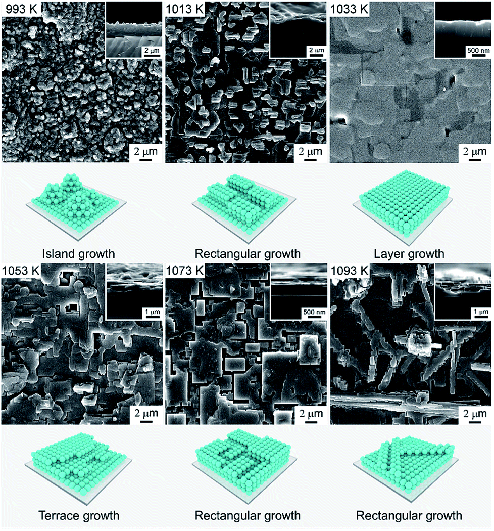 | ||
| Fig. 5 Surface and cross-section morphology of the NdBCO films prepared at Tdep = 993–1093 K and the corresponding growth modes. | ||
Fig. 6 shows a TEM bright-field (BF) image, a high resolution transmission electron microscopy (HRTEM) and selected area electron diffraction (SAED) pattern of the c-axis-oriented NdBCO film prepared at Tdep = 1033 K. In Fig. 6(a), it can be observed that the film and the substrate were combined smoothly. The SAED pattern (Fig. 6(c)) from the NdBCO grains in the square region confirms that the 〈001〉 direction of NdBCO film was normal to the substrate surface and that the 〈100〉 direction of NdBCO film was parallel to the interface, indicating c-axis-oriented growth. HRTEM image reveals a well crystallized film with ordered arrangement of atoms along [001] direction. A projection of a unit cell of NdBCO in [001] direction is indicated in the boxed region of Fig. 6(b). In addition, it can be noticed that there are small variations in contrast in some areas of the NdBCO film. These contrast changes indicates small variations in local crystal orientation.35 Such misorientations might have arisen during film growth, resulting in stress accumulation in the film.
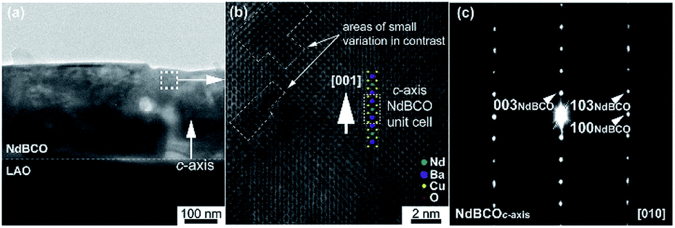 | ||
| Fig. 6 TEM characterization of the c-axis-oriented NdBCO film prepared at Tdep = 1033 K. (a) TEM BF image of the c-axis-oriented NdBCO film. (b) HRTEM image of the squared region in (a). (c) SAED pattern of the squared region in (a). A projection of a unit cell of NdBCO in [100] direction is depicted in the boxed region of (b). | ||
Fig. 7 shows a TEM bright-field (BF) image, a high resolution transmission electron microscopy (HRTEM) and selected area electron diffraction (SAED) patterns of the a, c-axis-co-oriented NdBCO film prepared at Tdep = 1053 K. The SAED patterns were collected at the same specimen tilting. A well-defined interface with a thickness of 1–2 atomic layers is observed as shown in HRTEM image (Fig. 7(b)), where the structures of NdBCO and LAO were closely aligned. The SAED patterns from the interface confirms that the 〈100〉 direction of the film was parallel to the 〈100〉 direction of the substrate, suggesting the a-axis epitaxial growth at the interface. Meanwhile, it further illustrates that the in-plane epitaxial relationship for the a-axis-oriented NdBCO grains was NdBCO [010]∥LAO [010] and NdBCO [001]∥LAO [001]. However, NdBCO grains marked by Fig. 7(d) and (e) represented two different growth orientations (the part near the substrate is a-axis oriented and the part near the surface is c-axis oriented). This phenomenon indicates that the a-axis-oriented grains nucleated firstly in the early deposition stage, because at the beginning of deposition, a transparent LAO substrate would reflect part of laser energy, and at the same time, the collision of the gas reactant molecules becomes more intense with higher energy laser irradiated, consuming the molecular kinetic energy, in that way, the deposited atoms without sufficient migration energy would tend to form a-axis configuration. As the deposition continued, the film with a certain thickness formed and began to absorb the major energy from the laser. Therefore, there was sufficient energy for atoms to migrate to form c-axis-oriented grains. This phenomenon of orientation change with the increase of thickness was also observed in β-SiC films deposited on (100) Si substrates via CVD.36,37 The TEM result is consistent with the description of the pole figure.
 | ||
| Fig. 7 TEM characterization of the a, c-axis-co-oriented NdBCO film prepared at Tdep = 1053 K. (a) TEM BF image of the a, c-axis-co-oriented NdBCO film. (b) HRTEM image of the interface. (c)–(e) SAED patterns taken from the (b, d and e) circular region in (a), respectively. | ||
Fig. 8 displays the temperature dependence of electrical resistivity (R) of the NdBCO films prepared at Tdep = 1033 K and 1053 K, respectively. The R of NdBCO film prepared at Tdep = 1033 K with c-axis-orientation shows metallic temperature dependence in the normal state and sharp zero resistance transition at critical transition (Tc) of 87 K. The R of NdBCO film prepared at Tdep = 1053 K shows a semiconductor resistivity behavior in the normal state and then appears a sharp drop at 56 K, which may be attributed to the structural inhomogeneity of the a, c-axis-co-oriented NdBCO film or the weak link originated from the high angle boundaries between a-axis and c-axis-oriented grains observed in Fig. 5.
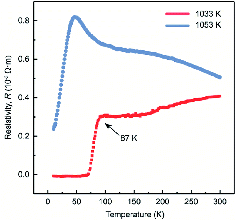 | ||
| Fig. 8 Temperature dependence of resistivity of the NdBCO films prepared at Tdep = 1033 K and 1053 K, respectively. | ||
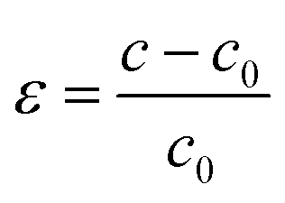
Fig. 9(a) shows the variation of the strain of the c-axis-oriented NdBCO grains calculated by the eqn (2)38 as a function of film thickness.
 | (2) |
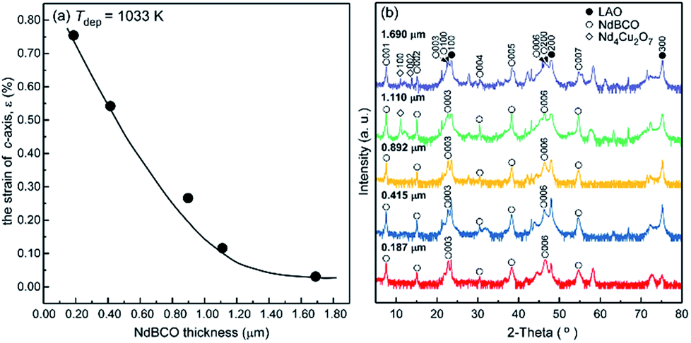 | ||
| Fig. 9 (a) The strain (ε) of c-axis as a function of film thickness. (b) XRD patterns of the NdBCO films with different thicknesses prepared at Tdep = 1033 K. | ||
4. Conclusions
c-Axis-oriented NdBCO films were epitaxially grown on (100) LAO single crystal substrates using laser CVD. As Tdep increased, the epitaxial growth orientation initially changed from a, c-axis to c-axis, and then back to a, c-axis again. c-Axis-oriented NdBCO films showed the Tc of 87 K with the minimum FWHM value of the φ-scan on the (116), indicating the highest crystallinity. The in-plane epitaxial growth relationship was NdBCO [100]∥LAO [010] and NdBCO [010]∥LAO [001] for the c-axis-oriented NdBCO grains, and NdBCO [010]∥LAO [010] and NdBCO [001]∥LAO [001] for the a-axis-oriented NdBCO grains with the 90° twinning structure. A c-axis-oriented NdBCO film exhibited a uniform dense surface, suggesting the layer growth mode. The TEM images of a, c-axis-co-oriented NdBCO film prepared at Tdep = 1053 K showed the orientation change from a-axis to c-axis as the film thickness increased. In the case of Tdep = 1033 K, the film strain was gradually relaxed and the film orientation changed from the c-axis to the a, c-axis, as the film thickness increased from 0.19 to 1.69 μm.Conflicts of interest
There are no conflicts to declare.Acknowledgements
This work was supported by National Natural Science Foundation of China, No. 51372188, No. 11602251 and No. 51521001 and the 111 Project (B13035). This research was also supported by the International Science & Technology Cooperation Program of China (2014DFA53090), and the Natural Science Foundation of Hubei Province, China (2016CFA006), and the Fundamental Research Funds for the Central Universities (WUT: 2017II43GX, 2017III032, 2017YB004, 2018III016), and Science Challenge Project (No. TZ2016001).Notes and references
- Y. M. Um, W. Jo, C. W. Seo, H. Cheong, S. H. Wee and S. I. Yoo, Supercond. Sci. Technol., 2007, 20, 925–929 CrossRef.
- M. Badaye, F. Wang, Y. Kanke, K. Fukushima, T. Morishita, M. Badaye, F. Wang, Y. Kanke and K. Fukushima, Appl. Phys. Lett., 1996, 2131, 10–13 Search PubMed.
- T. Kurian and T. Morishita, Europhys. Lett., 2003, 61, 129–133 CrossRef.
- H. M. Manasevit, Appl. Phys. Lett., 1968, 12, 156 CrossRef.
- A. Eulenburg, Phys. C, 1999, 312, 91–104 CrossRef.
- J. Kurian and T. Morishita, Supercond. Sci. Technol., 2003, 16, 422–425 CrossRef.
- C. Y. Tang, Y. Y. Chen, W. Li, L. J. Sun, X. Yao and M. Jirsa, Cryst. Growth Des., 2010, 10, 575–579 Search PubMed.
- Y. Kumagai, Y. Yoshida, M. Iwata and M. Hasegawa, Phys. C, 1998, 304, 35–42 CrossRef.
- M. Komatsu, F. Wang, N. Tanaka, H. Zama and T. Morishita, J. Cryst. Growth, 1999, 205, 277–283 CrossRef.
- R. Palai, E. J. Romans, R. W. Martin, F. T. Docherty and P. Maas, J. Phys. D: Appl. Phys., 2005, 38, 51–61 CrossRef.
- J. S. Bae, I. Yang and W. Jo, Jpn. J. Appl. Phys., 1999, 38, 923–925 CrossRef.
- U. S. Uccio and R. Vaglio, Phys. C, 2007, 462, 724–725 Search PubMed.
- I. Kim, W. Lee, Y. K. Park and J. Park, Appl. Phys. Lett., 1996, 68, 1859–1861 CrossRef.
- M. Salluzzo, A. Fragneto, G. M. De Luca, U. Scotti and X. Torrelles, Thin Solid Films, 2005, 486, 178–181 CrossRef.
- P. Zhao, S. Su, Y. Wang, C. Chen, Y. W. Mao, Z. L. Huang, Y. F. Niu, Y. L. Xu and T. Goto, Thin Solid Films, 2016, 599, 179–186 CrossRef.
- P. Zhao, Y. Wang and G. Takashi, Ceram. Int., 2015, 41, 3624–3630 CrossRef.
- P. Zhao, A. Ito and T. Goto, J. Electroceram., 2015, 34, 137–141 CrossRef.
- S. Zhang, Q. Xu, Q. Sun, P. Zhu, R. Tu, Z. Hu, M. Han, T. Goto, L. Zhang, J. Yan and S. Li, J. Am. Ceram. Soc., 2015, 3718, 3713–3718 CrossRef.
- R. Tu, G. Huo, T. Kimura and T. Goto, Thin Solid Films, 2010, 518, 6927–6932 CrossRef.
- P. Zhao, A. Ito, R. Tu and T. Goto, Surf. Coat. Technol., 2011, 205, 4079–4082 CrossRef.
- H. Cheng, R. Tu, S. Zhang, M. Han, T. Goto and L. Zhang, J. Eur. Ceram. Soc., 2017, 37, 509–515 CrossRef.
- P. Zhao, A. Ito and T. Goto, Surf. Coat. Technol., 2013, 235, 273–276 CrossRef.
- T. Goto, R. Banal and T. Kimura, Surf. Coat. Technol., 2007, 201, 5776–5781 CrossRef.
- F. K. Lotgering, J. Inorg. Nucl. Chem., 1960, 16, 100–108 CrossRef.
- W. Li, G. Li, B. Zhang, P. Chou, S. Liu and X. Ma, Phys. C, 2014, 501, 1–6 CrossRef.
- L. Liu, Z. Zhao, H. Liu and Y. Li, IEEE Trans. Appl. Supercond., 2010, 20, 1553–1556 CrossRef.
- F. Vassenden, G. Linker and J. Geerk, Phys. C, 1991, 175, 566–572 CrossRef.
- H. Izumi, K. Ohata, T. Sawada, T. Morishita and S. Tanaka, Jpn. J. Appl. Phys., 1991, 30, 1956–1958 CrossRef.
- S. Miyata, K. Matsuse, A. Ibi, T. Izumi, Y. Shiohara and T. Goto, Supercond. Sci. Technol., 2013, 26, 045020 CrossRef.
- K. Higashiyama, T. Ushida, H. Higa, I. Hirabayashi and S. Tanaka, Phys. C, 1993, 212, 101–109 CrossRef.
- S. Miyazawa and M. Mukaida, Appl. Phys. Lett., 1994, 2160, 2–5 Search PubMed.
- Y. L. He, G. C. Wang, A. J. Drehman, H. S. Jin, Y. He and G. Wang, Appl. Phys. Lett., 1990, 67, 12 Search PubMed.
- P. Zhao, A. Ito, T. Kato, D. Yokoe, T. Hirayama and T. Goto, Supercond. Sci. Technol., 2013, 26, 55020 CrossRef.
- P. Yossefov, G. E. Shter and G. S. Grader, Phys. C, 1997, 275, 299–310 CrossRef.
- H. W. Zandbergen, Phys. C, 2000, 329, 37–44 CrossRef.
- V. Radmilovic, U. Dahmen, D. Gao, C. R. Stoldt, C. Carraro and R. Maboudian, Diamond Relat. Mater., 2007, 16, 74–80 CrossRef.
- P. Zhu, Q. Xu, R. Chen, S. Zhang, M. Yang, R. Tu, L. Zhang, T. Goto, J. Yan and S. Li, J. Am. Ceram. Soc., 2017, 4, 1634–1641 CrossRef.
- W. Li, S. Li, G. Li, B. Zhang and P. Chou, IEEE Trans. Appl. Supercond., 2013, 23, 0–5 Search PubMed.
- J. D. Budai, W. Yang, N. Tamura, J. Chung, J. Z. Tischler, B. C. Larson, G. E. Ice, C. Park, D. P. Norton, A. L. Source, C. Road and L. Berkeley, Nat. Mater., 2008, 2, 487–492 CrossRef PubMed.
- R. Ramesh, A. Inam, D. M. Hwang, T. D. Sands, C. C. Chang, D. L. Hart, R. Ramesh, A. Inam, D. M. Hwang, T. D. Sands, C. C. Chang and D. L. Hart, Appl. Phys. Lett., 1991, 58, 1557 CrossRef.
- A. H. Carima, S. N. Basu and R. E. Muenchausen, Appl. Phys. Lett., 1991, 58, 871 CrossRef.
- A. Berenov, A. Purnell, A. Zhukov, N. Malde, Y. Bugoslavsky, L. F. Cohen, S. J. Foltyn and P. Dowden, Phys. C, 2002, 376, 683–686 CrossRef.
| This journal is © The Royal Society of Chemistry 2018 |