
 Open Access Article
 This Open Access Article is licensed under a
 Creative Commons Attribution 3.0 Unported Licence
Single-crystalline perovskite wafers with a Cr blocking layer for broad and stable light detection in a harsh environment†
Qian Wang‡
a,
Dongliang Bai‡a,
Zhiwen Jin *a and
Shengzhong (Frank) Liu*ab
*a and
Shengzhong (Frank) Liu*ab
aKey Laboratory of Applied Surface and Colloid Chemistry, Ministry of Education, Shaanxi Key Laboratory for Advanced Energy Devices, Shaanxi Engineering Lab for Advanced Energy Technology, School of Materials Science & Engineering, Shaanxi Normal University, Xi'an, 710119, P. R. China. E-mail: jinzhiwen@snnu.edu.cn
bDalian National Laboratory for Clean Energy, iChEM, Dalian Institute of Chemical Physics, Chinese Academy of Sciences, Dalian, 116023, P. R. China. E-mail: szliu@dicp.ac.cn
First published on 19th April 2018
Abstract
Herein, ultrathin (∼35 μm) CH3NH3PbI3 (MAPbI3) single-crystalline wafers have been successfully prepared by using an appropriate geometry-regulated dynamic-flow reaction system. The measurement results proved that the obtained wafers have high crystallinity, and showed broad light absorption from ultraviolet to near infrared (850 nm) which can be attributed to the indirect bandgap. Straight after, such an MAPbI3 wafer was used to fabricate high-quality photodetectors (PDs). On account of its faster carrier transport and significantly reduced defect density, the device exhibits a high photoresponse (R) of 5 A/W and short on/off response (0.039 s/0.017 s). Interestingly, by introducing a Cr interlayer between the MAPbI3 wafer and the Au electrode to avoid the migration of Au, the PD shows nearly no degradation when it works at 200 °C. Furthermore, the device performance shows very little degradation over the course of 60 days of storage under ambient conditions owing to its lack of grain boundaries. We believe the strategy reported here is very promising for achieving broad photodetection in a harsh environment.
Introduction
In recent years, halide perovskites (PVK) have attracted much attention due to their merits of high absorption coefficients, long carrier lifetimes, high electron and hole mobility, and low temperature solution processability, etc.1–8 These merits make the hybrid perovskite a strong competitor in the development of next-generation optoelectronic devices.9–14 Compared with the polycrystalline perovskites, the single-crystal perovskites show further enhanced optoelectronic properties due to their having a more long-range and ordered structure.15–19First of all, the redshifted absorption edge is observed due to its indirect-bandgap absorption transition with a bandgap of 60 meV smaller than the direct bandgap:20–22 the absorption coefficient corresponding to the below-bandgap transition is several orders of magnitude smaller than that of the above-gap transition.23 Hence, a thick perovskite single crystal could absorb more light through below-bandgap.24 Meanwhile, the single crystal perovskite show longer lifetime and much longer carrier diffusion length well above tens of micrometer due to the absence of grain boundaries and significantly reduced defect density.25,26 Moreover, the carrier mobility in single crystal is increased to 164 cm2 V−1 s−1.27 Therefore, the single crystal perovskite can provide not only a wider absorption spectrum but also better carrier transport efficiency, demonstrating its potential in applications as broad photodetector (PD).
In reality, the single crystal perovskite based PD indeed shows better photoelectronic performance than that of the PD made of polycrystalline perovskites,28 however, it is still not reach the commercial requirement. As is well known, the polycrystalline perovskites are stable at temperature not exceeding 85 °C.29 Meanwhile, the humidity and illumination also proved the main degradation trigger.30,31 For the single crystal perovskite, its stability is effectively enhanced under above-mentioned stress conditions for the lack of grain boundaries.32,33 However, in addition to the degradation of the perovskite itself, the device architecture is also found to greatly determine the stability of perovskite devices. It is reported that the considerable amounts of Au diffuse from the electrode to the perovskite layer, resulting in the irreversible performance loss.34,35 Hence, the issue whether the poor thermal stability of the single crystal perovskite PDs is caused by the diffusion of Au electrode should pay more attention.
In this study, we synthesized the ultrathin (∼35 μm) CH3NH3PbI3 (MAPbI3) singly-crystalline wafer, fabricated the corresponding PDs and investigated its stability. Of course, the device exhibits excellent performance with broad photodetection and outstanding ambient stability. Interestingly, the PD with ultrathin Cr interlayer between the wafer and Au electrode presents the excellent thermal stability without any obvious degradation. We believe this finding provides a new key variable component and paves the way toward using perovskite crystals in highly efficient photoelectric device.
Experimental section
MAPbI3 wafer preparation
Based on the inverse temperature crystallization of perovskites,36–38 PbI2 and MAI was dissolved in γ-butyrolactone (GBL) with solution concentration controlled at 1.1 M. The reaction system was placed in a flat container. Two thin glass slides were separated and aligned in parallel by two spacers with predefined separation to confine the crystal growth within the slit channel. The single-crystalline wafer thickness is defined by the spacers. When the MAPbI3 wafer is taken out from the growth solution, dipped into anhydrous diethylether to dissolve the solvent residue, and finally dried at 60 °C in a vacuum oven. Fig. S1† shows the photograph of one as-grown single crystals perovskite wafer.Device Fabrication
PDs were fabricated by directly thermal evaporation of 2 nm chromium and 60 nm-thick gold electrodes through a shadow mask onto the above obtained single crystal wafer which results in a channel width of 4000 μm and a channel lengths of 40 μm.Characterization
The morphology and cross-sectional image of the formed wafer were characterized by SEM (Hitachi S-4800). UV-Vis spectra were recorded using JASCO V-570 spectrophotometer. The phase identification was determined by using a Rifaku D/MAX-2004 XRD with Cu Kα radiation (λ = 1.54178 Å) operating at 40 KV and 60 mA. All electrical characterizations were recorded with a Keithley 4200 at room temperature in air. Prior to the use of monochromatic light, the spectral response of the mono-silicon solar cell was measured and normalized to the National Renewable Energy Laboratory (NREL) standards.Results and discussion
The ultrathin geometry-defined dynamic-flow reaction system was employed to synthesis single-crystalline MAPbI3 wafers,28 as shown in Fig. 1a. Usually, the lateral crystal growth can be limited by the inefficient long-range transportation of precursor ions along micrometer-size gap to continuously replenish the depleted precursors by crystal growth.20 Here, the dynamic flow is achieved using a peristaltic pump to warrant the crystal growth by enhanced the ion diffusion using constant fresh solution. Finally, the prepared MAPbI3 wafers, which were sandwiched by two paralleled glass slides, grow along with the slit channel easily. The thickness of the perovskite wafer was determined by the spacers between the two glass slides and wafer shape was defined by the design of slit channel. And the reaction process was finished in a heated beaker.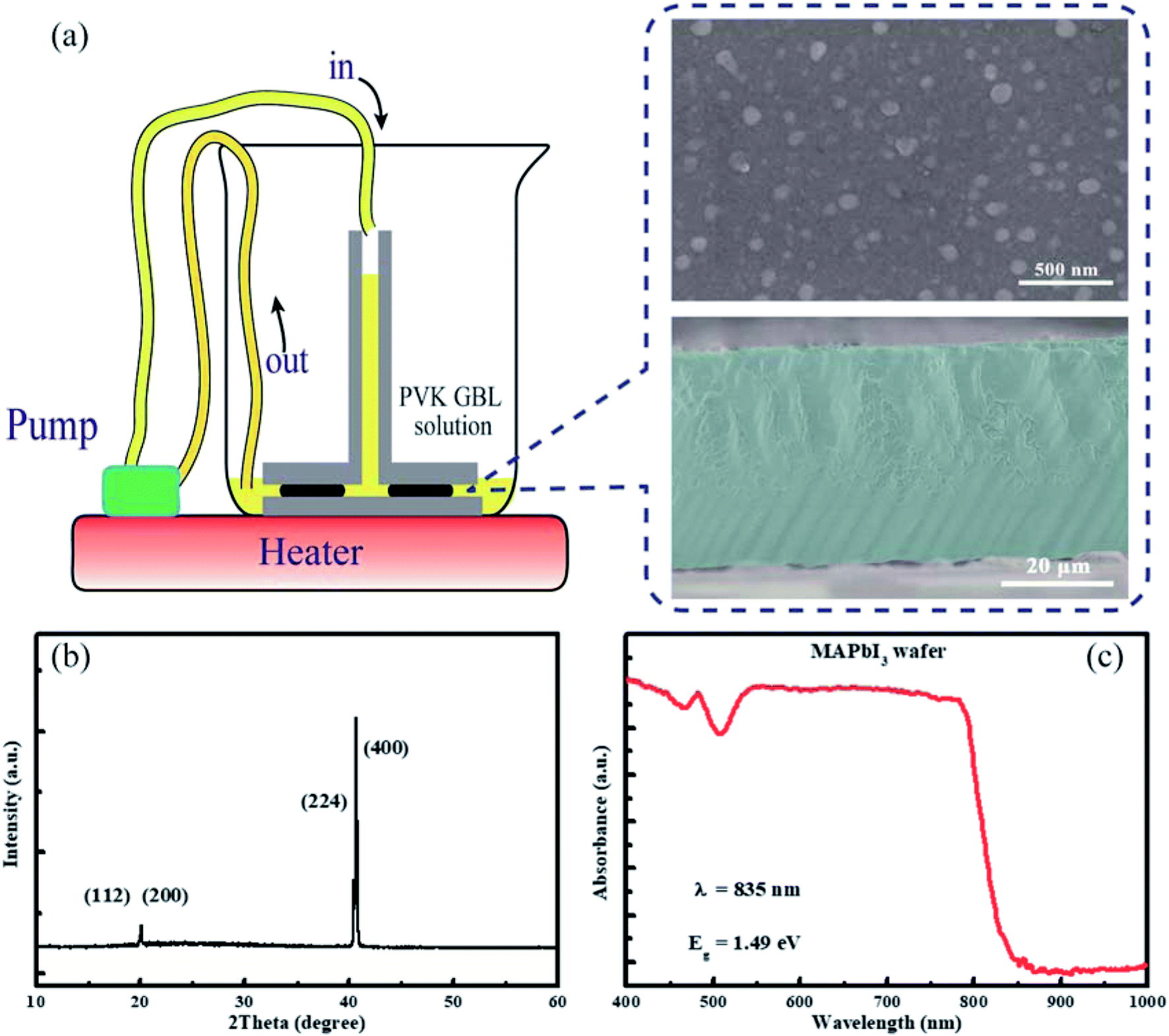 | ||
| Fig. 1 (a) The schematic illustration for preparing the single-crystalline MAPbI3 wafer with the inset showing corresponding surface and cross-section SEM images. (b) The XRD pattern and (c) absorption spectrum of MAPbI3 wafer. | ||
The inset of Fig. 1a and S2† give the surface and cross-section scanning electron microscopy (SEM) images of the fabricated MAPbI3 wafer. The surface morphology of the single-crystalline MAPbI3 wafer shows some nano-grain boundaries as reported by Mohammed et al.,39 which is very possibly due to the surface hydration and disorder facilitating the ion migration in MAPbI3 wafer from bulk to surface.40 The cross-section SEM images reveal the thickness of MAPbI3 wafer is about ∼35 μm. To detect the structural information and crystalline quality of MAPbI3 wafer, the X-ray diffraction (XRD) was employed. The XRD pattern of the synthesized single-crystalline wafer is shown in Fig. 1b, which provide evidence the as-grown MAPbI3 wafer was tetrahedral phase, and shown the (112) facets.41,42 By scanning (112) facets, diffractions corresponded to {112} crystal planes appearance. It should be mentioned that the synchronized appearance of {112} crystal planes was attributed to their adjacent 2θ value (the difference is ∼0.1°). Fig. 1c and S3† provide the absorption spectrum of the single crystal MAPbI3 wafer and the polycrystalline film, respectively. The absorption edge is at 850 nm for the single crystal wafer, showing the redshift compared with the polycrystalline film. This result demonstrates the single-crystalline MAPbI3 wafer possesses a narrower bandgap, which is in agreement with the report as told above.
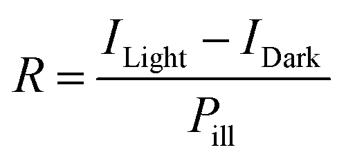
Followed, the MAPbI3 wafer was utilized to fabricate the PDs on account of the superior crystallization performance and optical properties. We have designed the PD structure, as shown in the inset of Fig. 2a: MAPbI3 wafer was regarded as the active layer, straight after, interdigitated ultra thin 2 nm Cr interlayer and 60 nm Au was directly thermal evaporation as electrode. The current–voltage (I–V) curves are measured at dark and under illumination 20 mW cm−2 using an LED laser emitting at 515 nm (shown in Fig. 2a). At 5 V, the dark current is 2.2 × 10⁻⁸ A, the larger dark current may caused by the grain boundaries in the surface and the in situ ion migration in the wafer as reported.43 While under light illumination, the device shows the photocurrent of 1.6 × 10⁻⁴ A. Obviously, the PD exhibits a high signal-to-noise ratio of about 104. Furthermore, one important parameter, responsivity (R), represents the ratio of the photocurrent to the incident light power, is defined to characterize the sensitivity of a PD.44,45 According to the following equation:46,47
 | (1) |
 | ||
| Fig. 2 (a) I–V curves of the PD made of MAPbI3 wafer with Cr metal as the interlayer between MAPbI3 wafer and Au electrode. (b) The temperature dependent light current stabilities of PDs with and without interlayer Cr (under illumination 20 mW cm−2 using an LED laser emitting at 515 nm). | ||
Fig. 2b compares the temperature stability of the devices with and without Cr interlayer. For the reference device, the photocurrent reduces the one order of magnitude when the temperature increased to 200 °C, which has been proved by the Au migration into the MAPbI3 at high temperature.34,50 Mostly, the deep trap states were produced by Au atoms within the perovskite semiconductor, which is beneficial for the nonradiative recombination and consequently degrades the photocurrent. However, for the Cr metal induced device, the photocurrent almost keeps constant with elevating temperature. The main reason is that Cr interlayer stop the Au metal diffusion preventing the reduced photoelectric performance.
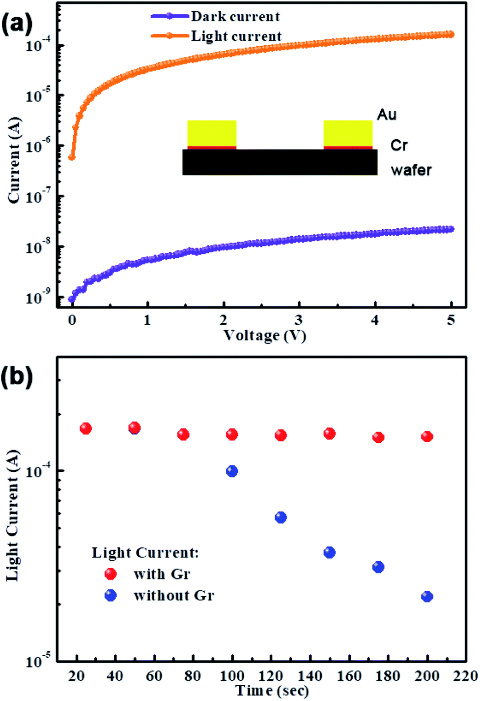
The time-dependent photoresponse of the above two PDs measured at different temperature in dark and under illumination 20 mW cm−2 using an LED laser emitting at 515 nm are depicted in Fig. 3. The results are in good agreement with Fig. 2b. At room temperature, the photocurrent of the reference PD rapidly increases to a peak value after turning on the light, and then drop to the initial when the light was turned off. The stable periodic response shows that the MAPbI3 wafer based PD has highly reproducible characteristics. When increase the temperature to 100 °C, it is obvious that the light current decrease but dark current increase, leading to the lower on/off ratio. More seriously, the high temperature of 200 °C deteriorates the current–time (I–t) curve, as shown in Fig. 3c, lowering the response of reference PD. This result indicates the poor thermal stability of PD without Cr interlayer, which should be caused by the above told facilitated Au diffusion facilitated at high temperature. However, the PD with Cr interlayer maintains high photoelectric responsiveness along with increasing the temperature, which shows an excellent thermal stability. Therefore, the Au diffusion from electrode to perovskite layer is the main reason for reducing the photoelectric performance of the PD. And the Cr interlayer indeed plays an important role in preventing Au diffusion and avoiding the degradation of photoelectric performance at high temperature.
 | ||
| Fig. 3 On/off switching properties at different temperature to compare the thermal stability of PDs: (a–c) without and (d–f) with Cr interlayer (in dark condition and under illumination 20 mW cm−2 using an LED laser emitting at 515 nm). | ||
A cycle of switching photocurrent curve was exhibited in Fig. 4a to investigate the response time of the Cr induced MAPbI3 wafer based PD with Cr interlayer. It is well known that the rise time and decay time are respectively defined as the time consumed when the current rise or fall to the 90% of the peak value.51–53 The rise time and decay time extracted from Fig. 4a are 0.039 s and 0.017 s, respectively, showing the fast response for the Cr induced MAPbI3 wafer the PD with Cr interlayer. The spectral selectivity of the PD is presented in Fig. 4b, which is consistent with its absorption spectrum and shows broad photodetection (UV to 850 nm).54,55 Furthermore, the stability of the PD with Cr interlayer is measured to test the practical application. Fig. 4c compares the I–t curves of the initial device and stored in ambient environment after two months at room temperature. Amusingly, the results demonstrate the excellent stability of the PD with Cr interlayer.
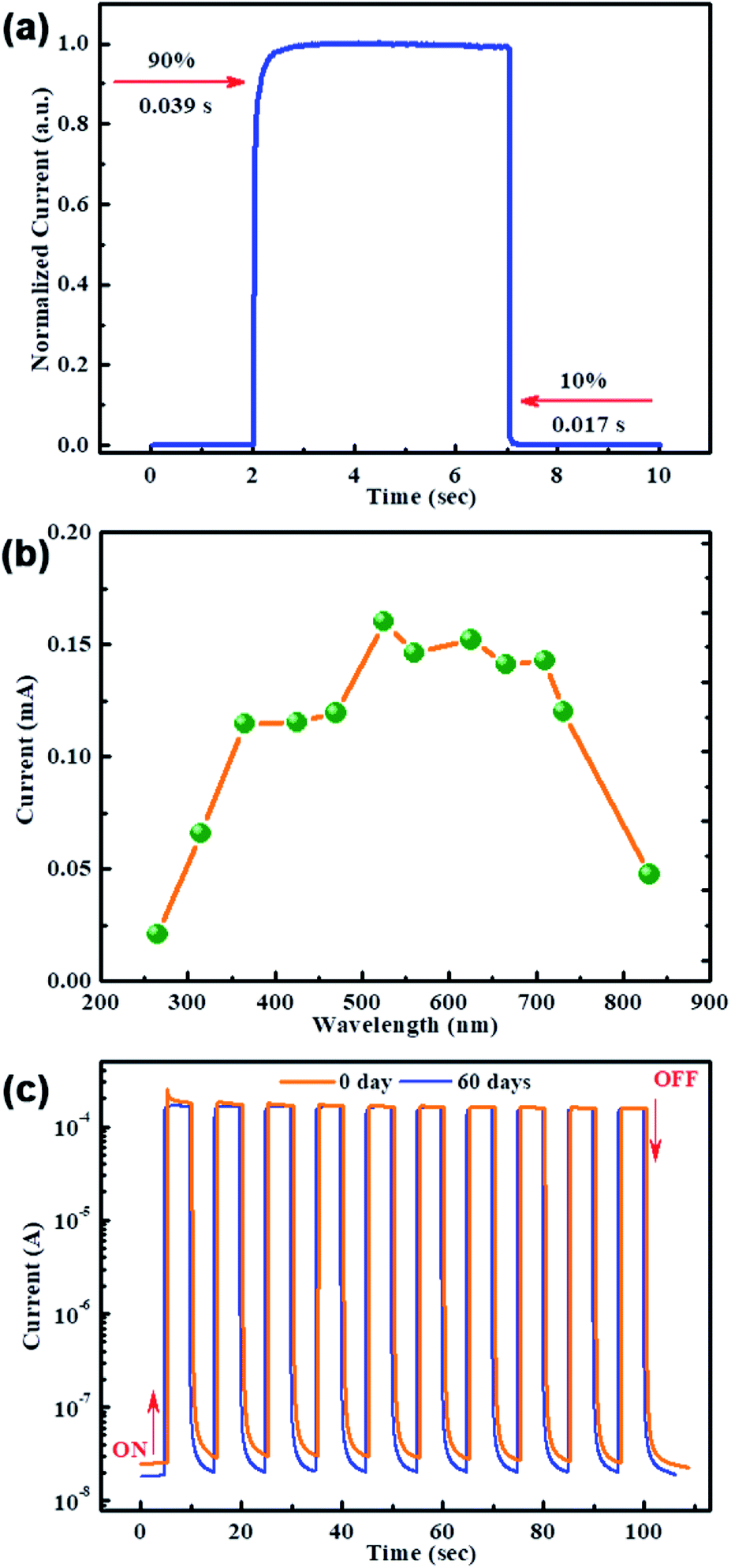 | ||
| Fig. 4 (a) Time-resolved photocurrent and (b) photocurrent spectrum of MAPbI3 wafer with Cr interlayer. (c) I–t curves for the initial and the PD stored in ambient condition after two months. | ||
Conclusions
In summary, we synthesized thin single-crystalline MAPbI3 wafer with extended absorption, and fabricated the corresponding PDs. It should be noted that an ultrathin Cr interlayer was induced sandwiched between the wafer and Au electrode to hinder the diffusion of Au electrode under high temperature. As a result, the fabricated device shows high photoresponse (5 A/W), short on/off response time (0.039 s/0.017 s) and broad photodetection region (UV to 850 nm). Moreover, the PD shows nearly no degradation when it works at 200 °C or storage under ambient conditions more than 60 days. This study demonstrates the potential for the application of the perovskite single-crystalline wafer in PDs.Author contributions statement
Q. W. and D. B. contributed equally to this work. Q. W. and D. B. performed the experiments, data analysis, and experimental planning. The project was conceived, planned, and supervised by Z. J. and S. L. The manuscript was written by Q. W., Z. J. and S. L. All authors reviewed the manuscript.Conflicts of interest
The authors declare no competing financial interests.Acknowledgements
This work was funded by the National Key Research and Development Program of China MOST (2017YFA0204800), Fundamental Research Funds for the Central Universities (GK201703026), the China Postdoctoral Science Foundation (2016M602759/2017M613052), National Natural Science Foundation of China (61704099/91733301), the Shaanxi Province Postdoctoral Science Foundation (2017BSHYDZZ04).References
- Y. Liu, et al., Adv. Mater., 2015, 27, 5176–5183 CrossRef CAS PubMed.
- Y. Fang, et al., Nat. Photonics, 2015, 9, 679 CrossRef CAS.
- Q. Wang, et al., Adv. Energy Mater., 2018 DOI:10.1002/aenm.201800007.
- G. X., et al., Science, 2013, 342, 344–347 CrossRef PubMed.
- Q. Han, et al., Adv. Mater., 2016, 28, 2253–2258 CrossRef CAS PubMed.
- X. Zhang, et al., ACS Appl. Mater. Interfaces, 2018, 10, 7145–7154 CAS.
- D. Bai, et al., ACS Energy Lett., 2018, 3, 970–978 CrossRef CAS.
- Q. Wang, et al., ACS Energy Lett., 2017, 2, 1479–1486 CrossRef CAS.
- H. S. Rao, et al., Adv. Mater., 2017, 29, 1602639 CrossRef PubMed.
- Y. Liu, et al., Adv. Opt. Mater., 2016, 4, 1829–1837 CrossRef CAS.
- Y. X. Chen, et al., J. Am. Ceram. Soc., 2016, 138, 16196–16199 CAS.
- G. A. Elbaz, et al., Nano Lett., 2017, 17, 1727–1732 CrossRef CAS PubMed.
- J. Jiang, et al., J. Mater. Chem. A, 2017, 5, 9514–9522 CAS.
- J. Feng, et al., Nano Energy, 2017, 36, 1–8 CrossRef CAS.
- A. J. Barker, et al., ACS Energy Lett., 2017, 2, 1416–1424 CrossRef CAS.
- B. Yang, et al., Adv. Funct. Mater., 2017, 27, 1700749 CrossRef.
- R. Dong, et al., Adv. Mater., 2015, 27, 1912–1918 CrossRef CAS PubMed.
- Q. Wang, et al., Adv. Mater., 2016, 28, 6734–6739 CrossRef CAS PubMed.
- M. Chen, et al., ACS Nano, 2017, 11, 6312–6318 CrossRef CAS PubMed.
- Z. Chen, et al., Nat. Commun., 2017, 8, 1890 CrossRef PubMed.
- T. Wang, et al., Energy Environ. Sci., 2017, 10, 509–515 CAS.
- E. M. Hutter, et al., Nat. Mater., 2016, 16, 115 CrossRef PubMed.
- C. Motta, et al., Nat. Commun., 2015, 6, 7026 CrossRef CAS PubMed.
- M. I. Saidaminov, et al., Adv. Mater., 2016, 28, 8144–8149 CrossRef CAS PubMed.
- D. Shi, et al., Science, 2015, 347, 519–522 CrossRef CAS PubMed.
- M. I. Saidaminov, et al., Nat. Commun., 2015, 6, 7586 CrossRef PubMed.
- Q. Dong, et al., Science, 2015, 347, 967–970 CrossRef CAS PubMed.
- Y. Liu, et al., Adv. Mater., 2016, 28, 9204–9209 CrossRef CAS PubMed.
- X. Li, et al., Nat. Chem., 2015, 7, 703–711 CrossRef CAS PubMed.
- J. Zhang, et al., Adv. Energy Mater., 2018 DOI:10.1002/aenm.201703246.
- J. Jiang, et al., Adv. Energy Mater., 2018, 8, 1701757 CrossRef.
- Y. Liu, et al., Adv. Sci., 2018, 5, 1700471 CrossRef PubMed.
- B. Murali, et al., J. Phys. Chem. Lett., 2017, 8, 137–143 CrossRef CAS PubMed.
- K. Domanski, et al., ACS Nano, 2016, 10, 6306–6314 CrossRef CAS PubMed.
- X. Hu, et al., Nanoscale, 2017, 9, 8274–8280 RSC.
- J. M. Kadro, et al., Sci. Rep., 2015, 5, 11654 CrossRef PubMed.
- T. Zhang, et al., Chem. Commun., 2015, 51, 7820–7823 RSC.
- M. I. Saidaminov, et al., Chem. Commun., 2015, 51, 17658–17661 RSC.
- S. P. Sarmah, et al., Nano Lett., 2017, 17, 2021–2027 CrossRef CAS PubMed.
- B. Murali, et al., ACS Energy Lett., 2016, 1, 1119–1126 CrossRef CAS.
- Z. Zuo, et al., Mater. Res. Bull., 2018, 99, 466–470 CrossRef CAS.
- A. De, et al., Nanoscale, 2017, 9, 16722–16727 RSC.
- T. Geske, et al., Adv. Funct. Mater., 2017, 27, 1702180 CrossRef.
- Z. Jin, et al., Adv. Mater., 2016, 28, 3697–3702 CrossRef CAS PubMed.
- Z. Jin, et al., ACS Appl. Mater. Interfaces, 2016, 8, 33043–33050 CAS.
- X. Zhang, et al., Nanoscale, 2017, 9, 6278–6285 RSC.
- L. Pang, et al., Part. Part. Syst. Charact., 2018, 35, 1700363 CrossRef.
- S. F. Leung, et al., Adv. Mater., 2018, 30, 1704611 CrossRef PubMed.
- E. Lafalce, et al., ACS Appl. Mater. Interfaces, 2016, 8, 35447–35453 CAS.
- S. Cacovich, et al., Nanoscale, 2017, 9, 4700–4706 RSC.
- Z. Jin, et al., Sci. Rep., 2014, 4, 4268 CrossRef PubMed.
- J. Zhang, et al., RSC Adv., 2017, 7, 36722–36727 RSC.
- Z. Gao, et al., Carbon, 2018, 128, 117–124 CrossRef CAS.
- Z. Jin and J. Wang, J. Mater. Chem. C, 2013, 1, 7996 RSC.
- Q. Wang, et al., Adv. Mater. Technol., 2017, 2, 1700185 CrossRef.
Footnotes |
| † Electronic supplementary information (ESI) available. See DOI: 10.1039/c8ra02709a |
| ‡ These authors contributed equally to this work. |
| This journal is © The Royal Society of Chemistry 2018 |